EP0019471A1 - Transistor-Schaltvorrichtung - Google Patents
Transistor-Schaltvorrichtung Download PDFInfo
- Publication number
- EP0019471A1 EP0019471A1 EP80301603A EP80301603A EP0019471A1 EP 0019471 A1 EP0019471 A1 EP 0019471A1 EP 80301603 A EP80301603 A EP 80301603A EP 80301603 A EP80301603 A EP 80301603A EP 0019471 A1 EP0019471 A1 EP 0019471A1
- Authority
- EP
- European Patent Office
- Prior art keywords
- transistor
- winding
- transformer
- current
- path
- Prior art date
- Legal status (The legal status is an assumption and is not a legal conclusion. Google has not performed a legal analysis and makes no representation as to the accuracy of the status listed.)
- Granted
Links
- 238000004804 winding Methods 0.000 claims abstract description 32
- 239000004065 semiconductor Substances 0.000 description 5
- 230000015556 catabolic process Effects 0.000 description 1
Images

Classifications
-
- H—ELECTRICITY
- H03—ELECTRONIC CIRCUITRY
- H03K—PULSE TECHNIQUE
- H03K17/00—Electronic switching or gating, i.e. not by contact-making and –breaking
- H03K17/04—Modifications for accelerating switching
- H03K17/042—Modifications for accelerating switching by feedback from the output circuit to the control circuit
- H03K17/0424—Modifications for accelerating switching by feedback from the output circuit to the control circuit by the use of a transformer
-
- H—ELECTRICITY
- H02—GENERATION; CONVERSION OR DISTRIBUTION OF ELECTRIC POWER
- H02M—APPARATUS FOR CONVERSION BETWEEN AC AND AC, BETWEEN AC AND DC, OR BETWEEN DC AND DC, AND FOR USE WITH MAINS OR SIMILAR POWER SUPPLY SYSTEMS; CONVERSION OF DC OR AC INPUT POWER INTO SURGE OUTPUT POWER; CONTROL OR REGULATION THEREOF
- H02M1/00—Details of apparatus for conversion
- H02M1/08—Circuits specially adapted for the generation of control voltages for semiconductor devices incorporated in static converters
-
- H—ELECTRICITY
- H03—ELECTRONIC CIRCUITRY
- H03K—PULSE TECHNIQUE
- H03K2217/00—Indexing scheme related to electronic switching or gating, i.e. not by contact-making or -breaking covered by H03K17/00
- H03K2217/0036—Means reducing energy consumption
Definitions
- the present invention relates to transistor switching circuits.
- the invention relates to transistor switching circuits for use in D.C. to D.C. convertors.
- the amount of charge stored in the base region of the output transistor during saturation can appreciably delay the switching-off of current in the output path unless steps are taken deliberately to remove this charge.
- said positive feedback is applied to the input path of said transistor by way of a further transistor.
- the means responsive to cessation of curren flow in one of said first and second windings may include a zener diode connected in series with said third windin
- a transistor switching circuit comprises a fir transistor, a transformer having a first winding connect in an output path of said first transistor, a second winding connected in the collector-emitter circuit of a driver transistor in such a sense as to provide positive feedback between said output path and an input circuit to said first transistor when said driver transistor is conducting, and voltage-breakdown means connected in series with a third winding of said transformer in said input circuit to said first transistor to provide a reverse-bias current for said first transistor when said driver transistor ceases to conduct.
- a D.C. to D.C. convertor may comprise two of said transistor switching circuits energised from a common D.C. source and operating alternately to supply current pulses to a common load.
- the current pulses may be width-modulated in such a way as to control the voltage applied to the load.
- the D.C. to D.C. convertor comprises two transistor switching circuits 1 and 2 operating under the control of respective driver circuits 3 and 4 to supply current pulses from a common D. C. source . (not shown) to respective output transformers 5 and 6.
- the respective secondary windings of these transformers are connected by way of respective rectifiers 7 and 8 to a common output path 9, which in turn may be connected to a load (not shown) by way of a filter circuit 14.
- the driver circuits 3 and 4 each receive a train of substantially constant amplitude rectangular pulses from a voltage control circuit 10, the pulses in the two trains being interlaced, and these pulses being width modulated in dependence upon the voltage at the output of the filter 14 such that in operation this voltage is maintained substantially constant.
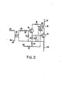
- each of the transistor switching circuits comprises an n-p-n power transistor 21 to switch current in an output path 23, 24 in dependence upon an input signal applied between a pair of inputs 25 and 26.
- the input pulse signal is applied by way of a transformer 27, a semiconductor diode 28 and a resistor 29 between the base electrode of the transistor 22 and the path 24.
- the base electrode of the transistor 22 is connected to the path 24 by way of a resistor 30, while the emitter electrode is connected to the path 24 by way of a resistor 31 and directly to the base electrode of the transistor 21.
- a feedback transformer 32 has its primary winding 33 connected in the output path 23, 24 and a secondary winding 34 connected by way of a semiconductor diode 35. between the path 24 and the collector electrode of the transistor 22. Another secondary winding 36 of the transformer 32 is connected by way of a semiconductor diode 37 bttween the path 24 and a positive supply line 38.
- the emitter electrode of the transistor 22 is connected to the junction between the winding 3 6 and the diode 37 by way of a semiconductor diode 39 and a semiconductor breakdown diode or zener diode 40.
- variable width input pulse signal applied between the inputs 25 and 26 will forward bias the diode 28 and the base-emitter diodes of the transistor 22 and the transistor 21, allowing current to flow through the colleccor-emitter path of the transistor 21 and the path 23 24.
- the consequent current flow through the primary winding 33 of the transformer 32 induces a current in the secondary winding 34 in such a sense that the diode 35 is forward biased, and induced current then flows through the collector-emitter path of the transistor 22 to augment the forward bias current flowing into the base electrode of the transistor 21.
- the turns ratio of the windings 33 and 34 may be arranged substantially to equal the current gain of the transistor 21 so as to provide an appropriate base drive current for the transistor 21, which completes switching-on and saturates.
- the transistor 21 When the stored charge has been removed the transistor 21 turns off and the current flow in the winding 33 of the transformer 32 ceases. Any remaining energy in the transformer 32 will then be dissipated by current flow to the positive supply rail 38 by way of the diode 37, or through a suitable zener diode (not shown) to the path 24 by way of the diode 37.
- the turns ratio of the windings 34 and 36 may be chosen to give a desired ratio between turn-on and turn-off current.
Landscapes
- Engineering & Computer Science (AREA)
- Power Engineering (AREA)
- Dc-Dc Converters (AREA)
- Electronic Switches (AREA)
Applications Claiming Priority (2)
| Application Number | Priority Date | Filing Date | Title |
|---|---|---|---|
| GB7917317 | 1979-05-18 | ||
| GB7917317 | 1979-05-18 |
Publications (2)
| Publication Number | Publication Date |
|---|---|
| EP0019471A1 true EP0019471A1 (de) | 1980-11-26 |
| EP0019471B1 EP0019471B1 (de) | 1984-03-21 |
Family
ID=10505241
Family Applications (1)
| Application Number | Title | Priority Date | Filing Date |
|---|---|---|---|
| EP80301603A Expired EP0019471B1 (de) | 1979-05-18 | 1980-05-16 | Transistor-Schaltvorrichtung |
Country Status (10)
| Country | Link |
|---|---|
| US (1) | US4322785A (de) |
| EP (1) | EP0019471B1 (de) |
| AU (1) | AU531699B2 (de) |
| BR (1) | BR8003079A (de) |
| CA (1) | CA1135336A (de) |
| DE (1) | DE3067106D1 (de) |
| IE (1) | IE49593B1 (de) |
| NZ (1) | NZ193646A (de) |
| PT (1) | PT71235A (de) |
| ZA (1) | ZA802746B (de) |
Cited By (3)
| Publication number | Priority date | Publication date | Assignee | Title |
|---|---|---|---|---|
| EP0068306A1 (de) * | 1981-06-23 | 1983-01-05 | HONEYWELL BULL ITALIA S.p.A. | Schrittmotorsteuerschaltung |
| FR2517498A1 (fr) * | 1981-12-02 | 1983-06-03 | Faiveley Sa | Amplificateur de courants impulsionnels de frequence elevee et procede s'y rapportant |
| EP0065135B1 (de) * | 1981-05-08 | 1985-03-27 | Siemens Aktiengesellschaft | Ansteuerschaltung für pulsgesteuerte Schalttransistoren |
Families Citing this family (16)
| Publication number | Priority date | Publication date | Assignee | Title |
|---|---|---|---|---|
| US4410810A (en) * | 1981-08-06 | 1983-10-18 | Gould Inc. | High speed transistor switching circuit |
| US4386311A (en) * | 1981-09-08 | 1983-05-31 | Motorola Inc. | Dual slope pulse width modulation regulator and control system |
| US4510563A (en) * | 1983-02-25 | 1985-04-09 | Sanyo Electric Co. Ltd. | Switching power supply |
| US4567378A (en) * | 1984-06-13 | 1986-01-28 | International Business Machines Corporation | Driver circuit for controlling signal rise and fall in field effect transistor processors |
| US4713740A (en) * | 1984-07-27 | 1987-12-15 | Sms Advanced Power, Inc. | Switch-mode power supply |
| US4629971A (en) * | 1985-04-11 | 1986-12-16 | Mai Basic Four, Inc. | Switch mode converter and improved primary switch drive therefor |
| JPS62196071A (ja) * | 1986-02-24 | 1987-08-29 | Fanuc Ltd | パワ−デバイス駆動用電源 |
| US5900683A (en) * | 1997-12-23 | 1999-05-04 | Ford Global Technologies, Inc. | Isolated gate driver for power switching device and method for carrying out same |
| CN101602762B (zh) * | 2008-06-10 | 2013-10-16 | 深圳迈瑞生物医疗电子股份有限公司 | 不对称菁类化合物、其制备方法及应用 |
| WO2014186776A1 (en) | 2013-05-17 | 2014-11-20 | Cirrus Logic, Inc. | Charge pump-based circuitry for bjt power supply |
| WO2014186765A1 (en) | 2013-05-17 | 2014-11-20 | Cirrus Logic, Inc. | Single pin control of bipolar junction transistor (bjt)-based power stage |
| WO2015017317A2 (en) | 2013-07-29 | 2015-02-05 | Cirrus Logic, Inc. | Two terminal drive of bipolar junction transistor (bjt) for switch-mode operation of a light emitting diode (led)-based bulb |
| US9504106B2 (en) | 2013-07-29 | 2016-11-22 | Cirrus Logic, Inc. | Compensating for a reverse recovery time period of a bipolar junction transistor (BJT) in switch-mode operation of a light-emitting diode (LED)-based bulb |
| US9504118B2 (en) | 2015-02-17 | 2016-11-22 | Cirrus Logic, Inc. | Resistance measurement of a resistor in a bipolar junction transistor (BJT)-based power stage |
| US9603206B2 (en) | 2015-02-27 | 2017-03-21 | Cirrus Logic, Inc. | Detection and control mechanism for tail current in a bipolar junction transistor (BJT)-based power stage |
| US9609701B2 (en) | 2015-02-27 | 2017-03-28 | Cirrus Logic, Inc. | Switch-mode drive sensing of reverse recovery in bipolar junction transistor (BJT)-based power converters |
Citations (5)
| Publication number | Priority date | Publication date | Assignee | Title |
|---|---|---|---|---|
| GB1456338A (en) * | 1974-12-16 | 1976-11-24 | Hasler Ag | Dc-dc converters |
| US3999086A (en) * | 1973-09-21 | 1976-12-21 | Telefonaktiebolaget L M Ericsson | Drive circuit for a controllable electronic switching element, for example, a power transistor |
| US4061931A (en) * | 1976-08-06 | 1977-12-06 | Boschert Associates | Switching regulator power supply main switching transistor turn off speed up circuit |
| US4070701A (en) * | 1974-10-21 | 1978-01-24 | General Electric Company | Inverter power supply |
| US4074146A (en) * | 1975-07-03 | 1978-02-14 | Burroughs Corporation | Load sharing modular power supply system |
Family Cites Families (6)
| Publication number | Priority date | Publication date | Assignee | Title |
|---|---|---|---|---|
| SU613464A1 (ru) * | 1971-07-30 | 1978-06-30 | Предприятие П/Я М-5374 | Преобразователь посто нного тока в посто нный |
| SU570963A1 (ru) | 1972-06-09 | 1977-08-30 | Предприятие П/Я М-5374 | Преобразователь посто нного тока посто нный |
| US3958168A (en) * | 1973-01-10 | 1976-05-18 | Kenneth Grundberg | Electronic control circuit |
| US3836836A (en) * | 1973-02-16 | 1974-09-17 | Us Army | Method for nuclear radiation hardening of dc-to-dc converters |
| US3962626A (en) * | 1974-11-26 | 1976-06-08 | Hughes Aircraft Company | Current driven inverter |
| US4070071A (en) * | 1976-02-09 | 1978-01-24 | The Goodyear Tire & Rubber Company | Traction element for removable track |
-
1980
- 1980-05-05 IE IE916/80A patent/IE49593B1/en unknown
- 1980-05-07 NZ NZ193646A patent/NZ193646A/xx unknown
- 1980-05-07 ZA ZA00802746A patent/ZA802746B/xx unknown
- 1980-05-12 US US06/148,813 patent/US4322785A/en not_active Expired - Lifetime
- 1980-05-13 PT PT71235A patent/PT71235A/pt unknown
- 1980-05-14 AU AU58403/80A patent/AU531699B2/en not_active Ceased
- 1980-05-16 DE DE8080301603T patent/DE3067106D1/de not_active Expired
- 1980-05-16 BR BR8003079A patent/BR8003079A/pt unknown
- 1980-05-16 EP EP80301603A patent/EP0019471B1/de not_active Expired
- 1980-05-16 CA CA000352103A patent/CA1135336A/en not_active Expired
Patent Citations (5)
| Publication number | Priority date | Publication date | Assignee | Title |
|---|---|---|---|---|
| US3999086A (en) * | 1973-09-21 | 1976-12-21 | Telefonaktiebolaget L M Ericsson | Drive circuit for a controllable electronic switching element, for example, a power transistor |
| US4070701A (en) * | 1974-10-21 | 1978-01-24 | General Electric Company | Inverter power supply |
| GB1456338A (en) * | 1974-12-16 | 1976-11-24 | Hasler Ag | Dc-dc converters |
| US4074146A (en) * | 1975-07-03 | 1978-02-14 | Burroughs Corporation | Load sharing modular power supply system |
| US4061931A (en) * | 1976-08-06 | 1977-12-06 | Boschert Associates | Switching regulator power supply main switching transistor turn off speed up circuit |
Cited By (3)
| Publication number | Priority date | Publication date | Assignee | Title |
|---|---|---|---|---|
| EP0065135B1 (de) * | 1981-05-08 | 1985-03-27 | Siemens Aktiengesellschaft | Ansteuerschaltung für pulsgesteuerte Schalttransistoren |
| EP0068306A1 (de) * | 1981-06-23 | 1983-01-05 | HONEYWELL BULL ITALIA S.p.A. | Schrittmotorsteuerschaltung |
| FR2517498A1 (fr) * | 1981-12-02 | 1983-06-03 | Faiveley Sa | Amplificateur de courants impulsionnels de frequence elevee et procede s'y rapportant |
Also Published As
| Publication number | Publication date |
|---|---|
| CA1135336A (en) | 1982-11-09 |
| NZ193646A (en) | 1983-07-15 |
| IE49593B1 (en) | 1985-10-30 |
| DE3067106D1 (en) | 1984-04-26 |
| IE800916L (en) | 1980-11-18 |
| AU531699B2 (en) | 1983-09-01 |
| BR8003079A (pt) | 1980-12-23 |
| EP0019471B1 (de) | 1984-03-21 |
| PT71235A (en) | 1980-06-01 |
| ZA802746B (en) | 1981-05-27 |
| AU5840380A (en) | 1980-11-20 |
| US4322785A (en) | 1982-03-30 |
Similar Documents
| Publication | Publication Date | Title |
|---|---|---|
| US4322785A (en) | Transistor switching circuit | |
| US4063307A (en) | Direct current power converter with start-up and protection circuits | |
| US4360744A (en) | Semiconductor switching circuits | |
| US3490027A (en) | Transistor converter amplifier circuit | |
| CA1184247A (en) | High speed transistor switching circuit | |
| US3361952A (en) | Driven inverter circuit | |
| US4308577A (en) | Base drive circuit | |
| US4593204A (en) | Driver circuits for gate turn-off thyristors and bipolar transistors | |
| US4319301A (en) | Circuits for electromagnet energization control | |
| US4916378A (en) | Inductive load discharge current recirculation circuit with selectable "fast" and "low" modes | |
| US4410809A (en) | Static induction transistor gate driving circuit | |
| GB2053606A (en) | Improvements in and relating to semiconductor switching circuits | |
| GB2050739A (en) | Transistor switching circuit | |
| US4609980A (en) | Switching power supply with transistor drive circuit | |
| JPH02254969A (ja) | スイッチトモード電源回路 | |
| US4639616A (en) | Circuit for controlling the base of a power transistor used in high tension switching | |
| CA1064576A (en) | High efficiency switching drive for a resonate power transformer | |
| US4272691A (en) | Generating electrical pulses | |
| JPH0715351Y2 (ja) | スイッチング電源装置 | |
| JPS5937667B2 (ja) | 電圧変換装置 | |
| KR100231441B1 (ko) | 자려식스위칭전원장치 | |
| JPS6040217B2 (ja) | 半導体スイッチ素子の駆動回路 | |
| SU1714767A1 (ru) | Формирователь управл ющих импульсов | |
| JP2563188B2 (ja) | 過電流保護機能付自励形コンバータ | |
| KR950009320Y1 (ko) | 과부하 보호기능과 경부하기능을 갖는 rcc형 스위칭전원의 구동회로 |
Legal Events
| Date | Code | Title | Description |
|---|---|---|---|
| PUAI | Public reference made under article 153(3) epc to a published international application that has entered the european phase |
Free format text: ORIGINAL CODE: 0009012 |
|
| AK | Designated contracting states |
Designated state(s): BE DE FR NL SE |
|
| 17P | Request for examination filed |
Effective date: 19810527 |
|
| R17P | Request for examination filed (corrected) |
Effective date: 19810526 |
|
| RAP1 | Party data changed (applicant data changed or rights of an application transferred) |
Owner name: THE GENERAL ELECTRIC COMPANY, P.L.C. |
|
| GRAA | (expected) grant |
Free format text: ORIGINAL CODE: 0009210 |
|
| AK | Designated contracting states |
Designated state(s): BE DE FR NL SE |
|
| REF | Corresponds to: |
Ref document number: 3067106 Country of ref document: DE Date of ref document: 19840426 |
|
| PGFP | Annual fee paid to national office [announced via postgrant information from national office to epo] |
Ref country code: FR Payment date: 19840427 Year of fee payment: 5 |
|
| ET | Fr: translation filed | ||
| PGFP | Annual fee paid to national office [announced via postgrant information from national office to epo] |
Ref country code: SE Payment date: 19840630 Year of fee payment: 5 Ref country code: BE Payment date: 19840630 Year of fee payment: 5 |
|
| PGFP | Annual fee paid to national office [announced via postgrant information from national office to epo] |
Ref country code: DE Payment date: 19840725 Year of fee payment: 5 |
|
| PLBE | No opposition filed within time limit |
Free format text: ORIGINAL CODE: 0009261 |
|
| STAA | Information on the status of an ep patent application or granted ep patent |
Free format text: STATUS: NO OPPOSITION FILED WITHIN TIME LIMIT |
|
| 26N | No opposition filed | ||
| PGFP | Annual fee paid to national office [announced via postgrant information from national office to epo] |
Ref country code: NL Payment date: 19850531 Year of fee payment: 6 |
|
| PG25 | Lapsed in a contracting state [announced via postgrant information from national office to epo] |
Ref country code: SE Effective date: 19860517 |
|
| PG25 | Lapsed in a contracting state [announced via postgrant information from national office to epo] |
Ref country code: BE Effective date: 19860531 |
|
| BERE | Be: lapsed |
Owner name: THE GENERAL ELECTRIC CY P.L.C. Effective date: 19860531 |
|
| PG25 | Lapsed in a contracting state [announced via postgrant information from national office to epo] |
Ref country code: NL Effective date: 19861201 |
|
| NLV4 | Nl: lapsed or anulled due to non-payment of the annual fee | ||
| PG25 | Lapsed in a contracting state [announced via postgrant information from national office to epo] |
Ref country code: FR Free format text: LAPSE BECAUSE OF NON-PAYMENT OF DUE FEES Effective date: 19870130 |
|
| PG25 | Lapsed in a contracting state [announced via postgrant information from national office to epo] |
Ref country code: DE Effective date: 19870203 |
|
| REG | Reference to a national code |
Ref country code: FR Ref legal event code: ST |
|
| EUG | Se: european patent has lapsed |
Ref document number: 80301603.9 Effective date: 19870225 |