EP0019941A1 - Système d'alignement pour système de projection rapetissant - Google Patents
Système d'alignement pour système de projection rapetissant Download PDFInfo
- Publication number
- EP0019941A1 EP0019941A1 EP80103125A EP80103125A EP0019941A1 EP 0019941 A1 EP0019941 A1 EP 0019941A1 EP 80103125 A EP80103125 A EP 80103125A EP 80103125 A EP80103125 A EP 80103125A EP 0019941 A1 EP0019941 A1 EP 0019941A1
- Authority
- EP
- European Patent Office
- Prior art keywords
- wafer
- slit
- pattern
- reticle
- reduction projection
- Prior art date
- Legal status (The legal status is an assumption and is not a legal conclusion. Google has not performed a legal analysis and makes no representation as to the accuracy of the status listed.)
- Granted
Links
Images

Classifications
-
- G—PHYSICS
- G03—PHOTOGRAPHY; CINEMATOGRAPHY; ANALOGOUS TECHNIQUES USING WAVES OTHER THAN OPTICAL WAVES; ELECTROGRAPHY; HOLOGRAPHY
- G03F—PHOTOMECHANICAL PRODUCTION OF TEXTURED OR PATTERNED SURFACES, e.g. FOR PRINTING, FOR PROCESSING OF SEMICONDUCTOR DEVICES; MATERIALS THEREFOR; ORIGINALS THEREFOR; APPARATUS SPECIALLY ADAPTED THEREFOR
- G03F9/00—Registration or positioning of originals, masks, frames, photographic sheets or textured or patterned surfaces, e.g. automatically
- G03F9/70—Registration or positioning of originals, masks, frames, photographic sheets or textured or patterned surfaces, e.g. automatically for microlithography
-
- H—ELECTRICITY
- H10—SEMICONDUCTOR DEVICES; ELECTRIC SOLID-STATE DEVICES NOT OTHERWISE PROVIDED FOR
- H10P—GENERIC PROCESSES OR APPARATUS FOR THE MANUFACTURE OR TREATMENT OF DEVICES COVERED BY CLASS H10
- H10P95/00—Generic processes or apparatus for manufacture or treatments not covered by the other groups of this subclass
Definitions
- This invention relates to improvements in a reduction projection aligner system for use in the semiconductor production.
- the reduction projection aligner system is used for the semiconductor production, and forms the patterns of semiconductor integrated circuits such as ICs and LSIs directly on wafers.
- the wafer and a reticle (a glass plate on which an original pattern is depicted) have been positioned independently of each other. More specifically, the reticle is positioned by visually detecting two typical portions on the reticle with a reticle positioning optical microscope and is fixed onto the body of the apparatus, while the wafer is positioned by visually detecting two typical portions on the wafer with a wafer positioning optical microscope and is fixed onto the body.
- the precision of the alignment between the reticle and the wafer depends principally on the positioning precision of the wafer, which forms a serious hindrance to the enhancemen of the alignment precision.
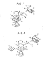
- a pattern for positioning formed on a wafer 4 by a preceding step is illuminated by a light guide 7 through a reference pattern 5 formed on an edge of a reticle 2 and further through a reduction lens 3, and using the reflected light, the positioning pattern on the wafer is focused on the reticle 2 contrariwise.
- the reference pattern 5 on the reticle 2 is illuminated by a light guide 6.
- the reflected lights from the wafer 4 and the reticle 2 are projected on the position of a slit 10 by a magnifying optical system 9, the distance of movement of the slit 10 is measured by a uniaxial movable table 12 and a measuring machine 13, and an output from a photodetector 11 corresponding to the position of the slit 10 is detected, whereby the relative positions of the reticle 2 and the wafer 4 are detected.
- the predetermined reference pattern 5 needs to be formed in a specified position on the reticle 2 separately from a circuit pattern and a reticle positioning pattern (which is used for positioning the reticle 2 to a holder 14), and it forms a serious hindrance in preparing the reticle.
- the arrangement error of the reference pattern 5 with respect to the circuit pattern becomes the alignment error between the reticle 2 and the wafer 4.
- an optical system for illuminating the reticle surface as consists of the light guide 6 and a mirror 8 is installed, the installation being very difficult.
- numeral 1 designates a condensing lens.
- This invention has been made in view of the above drawbacks, and has for its object to provide a reduction projection aligner system in which a positioning pattern on a wafer obtained through a reduction lens is detected by the use of a detecting optical system easy of installation, thereby to permit a high precision detection of the wafer position relative to the body of the system.
- a reduction projection aligner system which forms the patterns of semiconductor integrated circuits such as ICs and LSIs directly on wafers
- the positioning pattern on the wafer is optically magnified and projected and then focused
- the focused plane is scanned by a slit having its mechanical origin on the body of the system
- the brightness of light passing through the slit is photoelectrically converted in correspondence with the movement of the slit
- the distance from the mechanical origin of the slit to the positioning pattern of the wafer is measured, thereby to calculate the position of the wafer relative to the body of the reduction projection aligner system
- a reticle having the pattern to be formed anew is relatively moved so as to coincide with the wafer, to execute the so-called alignment.
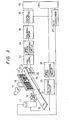
- FIG. 2 A conceptual diagram of a reduction projection aligner system according to this invention is shown in Figure 2.
- the system of this invention greatly differs from the system shown in Figure 1 in the following points.
- a part of the holder 14 to place a reticle 2' thereon is provided with a hole 15 so as to illuminate a pattern on a wafer by the light guide 7 through the reduction projection lens 3 similarly to the system shown in Figure 1. Therefore, the reticle 2' to be placed on the holder 14 does not need to be provided with the special reference mark 5 as shown in Figure 1, and it may merely have a structure adapted to transmit light through the edge thereof. Further, the light guide 6 for illuminating the reference mark 5 is unnecessary, , and one mirror 8 suffices.
- the pattern (for example, a rectilinear mark usually having a width of 6 ⁇ m or so) on the wafer as focused on the reticle is projected on the position of the slit 10 through the optical system 9.
- an origin sensor 16 is disposed in the movable range of the slit 10, and the distance from the origin of the slit 10 to the positioning pattern of the wafer is measured by the measuring machine 13.
- the origin sensor 16 is fixed on the body of the system, so that the distance of movement of the slit to the positioning pattern on the wafer after the slit has passed through the origin sensor 16 is gauged as the position of the wafer relative to the body of the system.
- FIG. 3 The details of a pattern detecting portion are shown in Figure 3.
- the slit 10 On the uniaxial movable table 12, there are placed the slit 10, a member to-be-detected 21 for the origin sensor 16, and a glass scale 13'.
- the glass scale 13' is movable only in the direction of arrow 22 with the movement of the uniaxial movable table 12.
- An index scale 19 is fixed at a predetermined spacing with respect to the glass scale 13'.
- the glass scale 13' and the index scale 19 are overlaid with gratings at equal spacings, and they are sandwiched in between a light source 17 as well as a lens 18 and a photodetector 20.
- the photodetector 20 Light projected from the light source 17 towards the photodetector 20 repeats brilliance and darkness each time the gratings of the glass scale 13' moves one pitch with respect to the index scale 19, and it is taken out as a sinusoidal signal. Since the output signal from the photodetector 20 is feeble as it is, it is amplified by a pre-amplifier 23. Further, the amplified signal is passed through a waveform shaping circuit 24 as well as a direction discriminator 28 and is indicated as a digital quantity by a digital counter 29.
- the origin sensor 16 there is employed by way of example a magnetic transducer which applies the principle of magnetic recording.
- the brilliance and darkness of light having passed through the slit is photoelectrically converted by the photomultiplier 11, the output of which is applied to an analog-to-digital converter 27.
- the A-D converter 27 digitizes the photomultiplier output in synchronism with the counter output from the digital counter 29, and applies the digital signal to a central processing unit 30.
- the CPU 30 receives the A-D converted value of the photomultiplier output in proportion to the count quantity of the-digital counter 29 and stores it therein.
- Figure 4 shows an example of the positioning pattern 31 on the wafer projected on the position of the slit 10.
- Figure 5 shows examples of signals stored in the CPU 30 at this time.
- the axis of abscissas represents the position X of the slit, while the axis of ordinates represents the A-D converted value Y of the photomultiplier output indicative of the intensity or the brilliance and darkness of the light passing through the slit.
- the digital value of the photomultiplier output begins to be received at a position X o at which the pulse from the origin sensor is received.
- the input data at the i-th count value X. becomes Y i .
- the central coordinates of the positioning pattern on the wafer as included in this output signal can be evaluated with, for example, the following method (refer to U. S. Patent 4153341).
- An arbitrary position X i of the slit is supposed as a tentative center, and data on both sides thereof amounting to 2.m are superposed to calculate Z i .
- Z i is calculated as follows: Among the changes of Z thus obtained, a point which gives the minimum value of Z becomes the central position of the pattern on the wafer.
- the positioning pattern on the wafer is magnified and focused through the optical lens, and the focused plane is scanned by the slit having its mechanical origin on the body of the system so as to photoelectrically detect the intensity of the light passing through the slit in accordance with the position of movement of the slit, thereby to measure the position of the wafer relative to the body at high precision, whereupon the wafer and the reticle positioned to the body with the separate detecting optical system are aligned.
- the position of the positioning pattern on the wafer is detected in the position in which the pattern is magnified and projected by the optical system of the simple construction including the reduction lens, whereby the high-precision positional detection has become possible.
- the detection and reproduction precision of the positioning pattern on the wafer in this invention is enhanced to double the precision in the system shown in Figure 1.
Landscapes
- Physics & Mathematics (AREA)
- General Physics & Mathematics (AREA)
- Exposure And Positioning Against Photoresist Photosensitive Materials (AREA)
- Projection-Type Copiers In General (AREA)
- Exposure Of Semiconductors, Excluding Electron Or Ion Beam Exposure (AREA)
- Length Measuring Devices By Optical Means (AREA)
Applications Claiming Priority (2)
| Application Number | Priority Date | Filing Date | Title |
|---|---|---|---|
| JP68971/79 | 1979-06-04 | ||
| JP6897179A JPS55162227A (en) | 1979-06-04 | 1979-06-04 | Microprojection exposure device |
Publications (2)
| Publication Number | Publication Date |
|---|---|
| EP0019941A1 true EP0019941A1 (fr) | 1980-12-10 |
| EP0019941B1 EP0019941B1 (fr) | 1985-10-02 |
Family
ID=13389057
Family Applications (1)
| Application Number | Title | Priority Date | Filing Date |
|---|---|---|---|
| EP80103125A Expired EP0019941B1 (fr) | 1979-06-04 | 1980-06-04 | Système d'alignement pour système de projection rapetissant |
Country Status (3)
| Country | Link |
|---|---|
| EP (1) | EP0019941B1 (fr) |
| JP (1) | JPS55162227A (fr) |
| DE (1) | DE3071137D1 (fr) |
Cited By (4)
| Publication number | Priority date | Publication date | Assignee | Title |
|---|---|---|---|---|
| EP0094041A1 (fr) * | 1982-05-07 | 1983-11-16 | Hitachi, Ltd. | Système d'alignement pour système de projection en réduction |
| GB2124397A (en) * | 1981-12-23 | 1984-02-15 | Canon Kk | Optical projection |
| DE3342719A1 (de) * | 1982-11-26 | 1984-05-30 | Canon K.K., Tokio/Tokyo | Belichtungsgeraet und belichtungsverfahren |
| FR2566217A1 (fr) * | 1984-05-28 | 1985-12-20 | Micro Controle | Procede et dispositif pour la reconnaissance d'un motif particulier d'une image |
Families Citing this family (2)
| Publication number | Priority date | Publication date | Assignee | Title |
|---|---|---|---|---|
| JPS57138134A (en) * | 1981-02-20 | 1982-08-26 | Nippon Kogaku Kk <Nikon> | Positioning device |
| JP2675528B2 (ja) * | 1994-09-30 | 1997-11-12 | 株式会社日立製作所 | 投影露光方法 |
Citations (3)
| Publication number | Priority date | Publication date | Assignee | Title |
|---|---|---|---|---|
| US3796497A (en) * | 1971-12-01 | 1974-03-12 | Ibm | Optical alignment method and apparatus |
| US3943359A (en) * | 1973-06-15 | 1976-03-09 | Hitachi, Ltd. | Apparatus for relatively positioning a plurality of objects by the use of a scanning optoelectric microscope |
| FR2296215A1 (fr) * | 1974-12-23 | 1976-07-23 | Ibm | Procede permettant de positionner des objets |
-
1979
- 1979-06-04 JP JP6897179A patent/JPS55162227A/ja active Granted
-
1980
- 1980-06-04 DE DE8080103125T patent/DE3071137D1/de not_active Expired
- 1980-06-04 EP EP80103125A patent/EP0019941B1/fr not_active Expired
Patent Citations (3)
| Publication number | Priority date | Publication date | Assignee | Title |
|---|---|---|---|---|
| US3796497A (en) * | 1971-12-01 | 1974-03-12 | Ibm | Optical alignment method and apparatus |
| US3943359A (en) * | 1973-06-15 | 1976-03-09 | Hitachi, Ltd. | Apparatus for relatively positioning a plurality of objects by the use of a scanning optoelectric microscope |
| FR2296215A1 (fr) * | 1974-12-23 | 1976-07-23 | Ibm | Procede permettant de positionner des objets |
Non-Patent Citations (1)
| Title |
|---|
| IBM TECHNICAL DISCLOSURE BULLETIN, Vol. 9, October 1966 New York (US) H.R. ROTTMAN: "Position Detecting Apparatus", pages 540 and 541. * The whole document * * |
Cited By (5)
| Publication number | Priority date | Publication date | Assignee | Title |
|---|---|---|---|---|
| GB2124397A (en) * | 1981-12-23 | 1984-02-15 | Canon Kk | Optical projection |
| EP0094041A1 (fr) * | 1982-05-07 | 1983-11-16 | Hitachi, Ltd. | Système d'alignement pour système de projection en réduction |
| DE3342719A1 (de) * | 1982-11-26 | 1984-05-30 | Canon K.K., Tokio/Tokyo | Belichtungsgeraet und belichtungsverfahren |
| FR2566217A1 (fr) * | 1984-05-28 | 1985-12-20 | Micro Controle | Procede et dispositif pour la reconnaissance d'un motif particulier d'une image |
| EP0166637A1 (fr) * | 1984-05-28 | 1986-01-02 | MICRO-CONTROLE, Société Anonyme dite: | Procédé et dispositif pour la reconnaissance d'un motif particulier d'une image |
Also Published As
| Publication number | Publication date |
|---|---|
| EP0019941B1 (fr) | 1985-10-02 |
| DE3071137D1 (en) | 1985-11-07 |
| JPS5748853B2 (fr) | 1982-10-19 |
| JPS55162227A (en) | 1980-12-17 |
Similar Documents
| Publication | Publication Date | Title |
|---|---|---|
| US4465368A (en) | Exposure apparatus for production of integrated circuit | |
| US4070116A (en) | Gap measuring device for defining the distance between two or more surfaces | |
| US4741622A (en) | Method and apparatus for detecting diversion | |
| JP2734004B2 (ja) | 位置合わせ装置 | |
| US4566795A (en) | Alignment apparatus | |
| US4419013A (en) | Phase contrast alignment system for a semiconductor manufacturing apparatus | |
| KR100299930B1 (ko) | 물체의차원을측정하는장치및그에사용되는척도기 | |
| US5767523A (en) | Multiple detector alignment system for photolithography | |
| US4380395A (en) | Reduction projection aligner system | |
| EP0019941A1 (fr) | Système d'alignement pour système de projection rapetissant | |
| JPH0258766B2 (fr) | ||
| KR100295477B1 (ko) | 물체의치수를측정하는장치 | |
| JP3203676B2 (ja) | 投影露光装置 | |
| EP0094041B1 (fr) | Système d'alignement pour système de projection en réduction | |
| Zhou et al. | Subnanometer alignment system for x‐ray lithography | |
| JP3146568B2 (ja) | パターン認識装置 | |
| JP3209186B2 (ja) | 露光装置及び方法 | |
| US4808807A (en) | Optical focus sensor system | |
| KR100249789B1 (ko) | 정전용량 센서를 이용한 레티클 수평/수직 정렬방법 | |
| SU905633A1 (ru) | Устройство дл контрол размерных параметров топологии фотошаблонов | |
| JP3209886B2 (ja) | 計測装置 | |
| JPH03231104A (ja) | 微小寸法測定方法 | |
| JPH0547091B2 (fr) | ||
| KR950004369A (ko) | 투영 노광 장치 및 방법 | |
| JPH11195605A (ja) | 露光装置及び方法 |
Legal Events
| Date | Code | Title | Description |
|---|---|---|---|
| PUAI | Public reference made under article 153(3) epc to a published international application that has entered the european phase |
Free format text: ORIGINAL CODE: 0009012 |
|
| AK | Designated contracting states |
Designated state(s): DE FR GB NL |
|
| 17P | Request for examination filed |
Effective date: 19810522 |
|
| GRAA | (expected) grant |
Free format text: ORIGINAL CODE: 0009210 |
|
| AK | Designated contracting states |
Designated state(s): DE FR GB NL |
|
| REF | Corresponds to: |
Ref document number: 3071137 Country of ref document: DE Date of ref document: 19851107 |
|
| ET | Fr: translation filed | ||
| PLBE | No opposition filed within time limit |
Free format text: ORIGINAL CODE: 0009261 |
|
| STAA | Information on the status of an ep patent application or granted ep patent |
Free format text: STATUS: NO OPPOSITION FILED WITHIN TIME LIMIT |
|
| 26N | No opposition filed | ||
| PG25 | Lapsed in a contracting state [announced via postgrant information from national office to epo] |
Ref country code: GB Effective date: 19890604 |
|
| GBPC | Gb: european patent ceased through non-payment of renewal fee | ||
| PG25 | Lapsed in a contracting state [announced via postgrant information from national office to epo] |
Ref country code: FR Free format text: LAPSE BECAUSE OF NON-PAYMENT OF DUE FEES Effective date: 19900228 |
|
| REG | Reference to a national code |
Ref country code: FR Ref legal event code: ST |
|
| PGFP | Annual fee paid to national office [announced via postgrant information from national office to epo] |
Ref country code: DE Payment date: 19970826 Year of fee payment: 18 |
|
| PGFP | Annual fee paid to national office [announced via postgrant information from national office to epo] |
Ref country code: NL Payment date: 19980630 Year of fee payment: 19 |
|
| PG25 | Lapsed in a contracting state [announced via postgrant information from national office to epo] |
Ref country code: DE Free format text: LAPSE BECAUSE OF NON-PAYMENT OF DUE FEES Effective date: 19990401 |
|
| PG25 | Lapsed in a contracting state [announced via postgrant information from national office to epo] |
Ref country code: NL Free format text: LAPSE BECAUSE OF NON-PAYMENT OF DUE FEES Effective date: 20000101 |
|
| NLV4 | Nl: lapsed or anulled due to non-payment of the annual fee |
Effective date: 20000101 |