EP0019976B1 - Dispositif d'affichage - Google Patents
Dispositif d'affichage Download PDFInfo
- Publication number
- EP0019976B1 EP0019976B1 EP19800200478 EP80200478A EP0019976B1 EP 0019976 B1 EP0019976 B1 EP 0019976B1 EP 19800200478 EP19800200478 EP 19800200478 EP 80200478 A EP80200478 A EP 80200478A EP 0019976 B1 EP0019976 B1 EP 0019976B1
- Authority
- EP
- European Patent Office
- Prior art keywords
- transistor
- display device
- picture elements
- electrode
- row
- Prior art date
- Legal status (The legal status is an assumption and is not a legal conclusion. Google has not performed a legal analysis and makes no representation as to the accuracy of the status listed.)
- Expired
Links
- 239000011159 matrix material Substances 0.000 claims description 25
- 239000003990 capacitor Substances 0.000 claims description 14
- PNEYBMLMFCGWSK-UHFFFAOYSA-N aluminium oxide Inorganic materials [O-2].[O-2].[O-2].[Al+3].[Al+3] PNEYBMLMFCGWSK-UHFFFAOYSA-N 0.000 claims description 10
- 239000000463 material Substances 0.000 claims description 7
- 239000010409 thin film Substances 0.000 claims description 7
- 150000003839 salts Chemical class 0.000 claims description 3
- 230000000694 effects Effects 0.000 description 4
- PCHJSUWPFVWCPO-UHFFFAOYSA-N gold Chemical compound [Au] PCHJSUWPFVWCPO-UHFFFAOYSA-N 0.000 description 4
- 239000010931 gold Substances 0.000 description 4
- 229910052737 gold Inorganic materials 0.000 description 4
- 230000003446 memory effect Effects 0.000 description 3
- OAICVXFJPJFONN-UHFFFAOYSA-N Phosphorus Chemical compound [P] OAICVXFJPJFONN-UHFFFAOYSA-N 0.000 description 2
- 238000006243 chemical reaction Methods 0.000 description 2
- 238000010276 construction Methods 0.000 description 2
- 238000010586 diagram Methods 0.000 description 2
- 239000010408 film Substances 0.000 description 2
- 239000011521 glass Substances 0.000 description 2
- VRXAJMCFEOESJO-UHFFFAOYSA-L 1-heptyl-4-(1-heptylpyridin-1-ium-4-yl)pyridin-1-ium;dibromide Chemical compound [Br-].[Br-].C1=C[N+](CCCCCCC)=CC=C1C1=CC=[N+](CCCCCCC)C=C1 VRXAJMCFEOESJO-UHFFFAOYSA-L 0.000 description 1
- 102000001690 Factor VIII Human genes 0.000 description 1
- 108010054218 Factor VIII Proteins 0.000 description 1
- 239000007795 chemical reaction product Substances 0.000 description 1
- 150000001875 compounds Chemical class 0.000 description 1
- 230000001419 dependent effect Effects 0.000 description 1
- 238000000034 method Methods 0.000 description 1
- 230000033116 oxidation-reduction process Effects 0.000 description 1
- 239000002244 precipitate Substances 0.000 description 1
- 238000006479 redox reaction Methods 0.000 description 1
- 238000007789 sealing Methods 0.000 description 1
- 238000004904 shortening Methods 0.000 description 1
- 239000000126 substance Substances 0.000 description 1
- XOLBLPGZBRYERU-UHFFFAOYSA-N tin dioxide Chemical compound O=[Sn]=O XOLBLPGZBRYERU-UHFFFAOYSA-N 0.000 description 1
- 229910001887 tin oxide Inorganic materials 0.000 description 1
Images
Classifications
-
- G—PHYSICS
- G09—EDUCATION; CRYPTOGRAPHY; DISPLAY; ADVERTISING; SEALS
- G09G—ARRANGEMENTS OR CIRCUITS FOR CONTROL OF INDICATING DEVICES USING STATIC MEANS TO PRESENT VARIABLE INFORMATION
- G09G3/00—Control arrangements or circuits, of interest only in connection with visual indicators other than cathode-ray tubes
- G09G3/20—Control arrangements or circuits, of interest only in connection with visual indicators other than cathode-ray tubes for presentation of an assembly of a number of characters, e.g. a page, by composing the assembly by combination of individual elements arranged in a matrix no fixed position being assigned to or needed to be assigned to the individual characters or partial characters
- G09G3/34—Control arrangements or circuits, of interest only in connection with visual indicators other than cathode-ray tubes for presentation of an assembly of a number of characters, e.g. a page, by composing the assembly by combination of individual elements arranged in a matrix no fixed position being assigned to or needed to be assigned to the individual characters or partial characters by control of light from an independent source
- G09G3/38—Control arrangements or circuits, of interest only in connection with visual indicators other than cathode-ray tubes for presentation of an assembly of a number of characters, e.g. a page, by composing the assembly by combination of individual elements arranged in a matrix no fixed position being assigned to or needed to be assigned to the individual characters or partial characters by control of light from an independent source using electrochromic devices
-
- G—PHYSICS
- G02—OPTICS
- G02F—OPTICAL DEVICES OR ARRANGEMENTS FOR THE CONTROL OF LIGHT BY MODIFICATION OF THE OPTICAL PROPERTIES OF THE MEDIA OF THE ELEMENTS INVOLVED THEREIN; NON-LINEAR OPTICS; FREQUENCY-CHANGING OF LIGHT; OPTICAL LOGIC ELEMENTS; OPTICAL ANALOGUE/DIGITAL CONVERTERS
- G02F1/00—Devices or arrangements for the control of the intensity, colour, phase, polarisation or direction of light arriving from an independent light source, e.g. switching, gating or modulating; Non-linear optics
- G02F1/01—Devices or arrangements for the control of the intensity, colour, phase, polarisation or direction of light arriving from an independent light source, e.g. switching, gating or modulating; Non-linear optics for the control of the intensity, phase, polarisation or colour
- G02F1/15—Devices or arrangements for the control of the intensity, colour, phase, polarisation or direction of light arriving from an independent light source, e.g. switching, gating or modulating; Non-linear optics for the control of the intensity, phase, polarisation or colour based on an electrochromic effect
- G02F1/163—Operation of electrochromic cells, e.g. electrodeposition cells; Circuit arrangements therefor
-
- G—PHYSICS
- G09—EDUCATION; CRYPTOGRAPHY; DISPLAY; ADVERTISING; SEALS
- G09G—ARRANGEMENTS OR CIRCUITS FOR CONTROL OF INDICATING DEVICES USING STATIC MEANS TO PRESENT VARIABLE INFORMATION
- G09G2300/00—Aspects of the constitution of display devices
- G09G2300/08—Active matrix structure, i.e. with use of active elements, inclusive of non-linear two terminal elements, in the pixels together with light emitting or modulating elements
- G09G2300/0809—Several active elements per pixel in active matrix panels
- G09G2300/0842—Several active elements per pixel in active matrix panels forming a memory circuit, e.g. a dynamic memory with one capacitor
Definitions
- the invention relates to a display device comprising a display medium between two supporting plates, of which one supporting plate has a matrix of display elements, a matrix of strip-shaped row electrodes and strip-shaped column electrodes insulated from each other at the crossings, which row electrodes and column electrodes are situated between the rows and columns of the matrix of display elements, a matrix of thin-film transistor circuits, in which each circuit is formed by a first transistor, a second transistor and a capacitor, of which first transistor the gate is connected to a strip-shaped row electrode, the drain is connected to a strip-shaped column electrode and the source is connected to the gate of the second transistor, of which second transistor the drain is connected to a display element, the gate is connected to a terminal of the capacitor and the source is connected to the other terminal of the capacitor, which source of the second transistor is furthermore connected to a power electrode, and the other supporting plate. of which has a counter electrode which is common for all display elements.
- the invention also relates to a device for driving such a display device.
- Such a display device is disclosed in United States Patent Specification 4,042,854.
- TFT-matrix Thin Film Transistor matrix
- Each element of the TFT matrix comprises two transistors and a capacitor.
- the rows of the matrix of picture elements are successively driven, all elements of a driven row being simultaneously provided with information.
- the transistors of the TFT matrix form the circuit elements which are necessary for addressing and providing the rows of a matrix of picture elements with information.
- An electroluminescent phosphor layer shows no memory effect so that the information which is presented during the driving of a row has to be stored during the time which is necessary to drive the remaining rows, the so- called frame time.
- the capacitors of the TFT-matrix serve to store the information.
- Writing of the picture elements occurs by applying a voltage across strip-shaped power electrodes extending parallel to the columns of picture elements and a counter electrode which is common for the picture elements.
- a result of the absence of memory effect of the electroluminescent phosphor layer is that the picture elements must be energized continuously.
- such a display device is not suitable for use with an electrochromic display medium instead of an electroluminescent display medium due to a number of essential differences between these two display media.
- an electrochromic display device the display effect occurs as a result of a passage of current through the electrochromic material, the contrast being determined by the time duration and the value of the passage of the current. As a result of this it is not possible to energize driven picture elements during a frame time since this would cause contrast differences.
- an electrochromic material shows memory effect so that it is possible in principle to drive, to provide with information and to write line by line. In this case the capacitors and one transistor of each TFT circuit belonging to each picture element may be omitted.
- Writing individual lines has disadvantages in that the strip-shaped electrodes for the power supply have a rather high resistance.
- the high current densities necessary for the electrochromic display effect in fact cause a considerable voltage drop across the strip-shaped power electrodes, which gives rise to contrast differences.
- the energisation line by line has for its result that the overall time necessary for driving and exciting all lines becomes larger since for writing a current must be passed through the display medium for a given period of time.
- a display device of the kind mentioned in the opening paragraph is characterized in that the power electrode is formed by a conductive layer which is provided on one supporting plate and has an insulating layer and which is connected through apertures in the insulating layer to the source of the second transistor of each thin-film transistor circuit.
- the power electrode is formed by a conductive layer which is provided on one supporting plate and has an insulating layer and which is connected through apertures in the insulating layer to the source of the second transistor of each thin-film transistor circuit.
- a display device in accordance with the invention is particularly suitable for use with an electrochromic material as a display medium and especially a solution of a viologen salt.
- Displaying by means of a viologen salt as a display medium is based on a chemical reaction in which coloured contrast-rich pictures are obtained.
- a suitable device for driving a display device in accordance with the invention which device has first means to drive a row of picture elements, second means to provide a driven row of picture elements with information, third means to write the information and control means to energize the first, second and third means, is characterized in that the control means successively energize the first and second means for all rows of picture elements and then energize the third means for all the rows in common.
- the overall time required for driving and writing the rows is nxt, +nxt 2 , where n is the number of rows of picture elements, t, is the time for driving a row and t 2 is the time for writing a row. Since the display device in accordance with the invention is constructed with one common power electrode, writing row by row is no longer possible since otherwise contrast differences occur. The rows of picture elements are now first driven successively and provided with information after which all rows are written simultaneously. The overall time for driving and writing in this case is nxt 1 + t 2 .
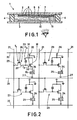
- Fig. 1 is a diagrammatic sectional view of a display device according to the invention.
- the display device 1 comprises two parallel glass supporting plates 2 and 3 which are kept spaced apart by sealing means 4 in the form of a frame with which the device 1 is also sealed.
- a common power electrode 6 of gold is provided on the supporting plate 2 and successively a common power electrode 6 of gold, an insulating layer 7 of aluminium oxide and a layer with TFT circuits and picture elements denoted diagrammatically by 9.
- Via apertures 8 in the insulating layer 7 the layer 9 is connected to the power electrode 6.
- a transparent counter electrode 10 of tin oxide is provided on the supporting plate 3.
- the display device 1 is filled with a diheptylviologendibromide which belongs to the group 4,4'-dipyridinium compounds (viologens).
- the display effect is based on a reduction oxidation reaction in which the reaction product is a coloured insoluble film. In principle the chemical reaction occurs as follows: oxidation reduction The precipitate of ABr has a purple colour.
- viologens are known per se from the book "Non-emissive Electrooptic Displays" pp, 201-211. The operation of the picture display device will be described in detail with reference to Fig. 2, which shows diagrammatically the construction of the layer with TFT-circuits.
- the layer comprises a matrix of strip-shaped row electrodes 20 and strip-shaped column electrodes 21 which are insulated from each other at the crossings.
- the strip-shaped row electrodes 20 constitute the address electrodes and the strip-shaped column electrodes 21 constitute the information electrodes of the device.
- a TFT-circuit 23 and a picture element 24 are provided in each aperture of the matrix of row electrodes 20 and column electrodes 21.
- the TFT-circuits 23, the row electrodes 20 and the column electrodes 21 are covered with an insulating layer so that only the actual picture elements 24 are in direct contact with the electrochromic material 25. All picture elements 24 have a common power electrode and a common counter electrode which are shown diagrammatically by the circles 26 and 27, respectively.
- Each TFT-circuit is formed by two transistors T 1 , T 2 and a capacitor C s .
- the gate 28 and the source 29 of T are connected to a row electrode 20 and a column electrode 21, respectively.
- the drain 30 of T is connected to the gate of T 2 and to the capacitor C s .
- the source 32 of T 2 and the capacitor C s are connected to the earthed power electrode 26 which is common for all the picture elements 24.
- the drain 33 of T2 is connected to a picture element 24.
- the operation of the display device is as follows. If a row electrode 20 is driven with a positive voltage pulse, the transistors T 1 , which are connected to the driven row electrode 20, becomes conductive. This has for its result that the pulse-shaped information which is presented to the column electrodes 21 is stored in the capacitors C s . In this manner all electrodes 20 are driven successively, all elements of one row being simultaneously provided with information via the column electrodes 21. Dependent on the presence or absence of a voltage across the capacitors C s and hence a voltage at the gate of T 2 , the transistors T 2 become conductive. As a result of this a conductive connection is produced between the power electrode 26 and a picture element 24.
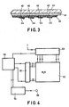
- Fig. 3 shows diagrammatically the connection of the TFT-circuits with the common power electrode.
- a power electrode 41 which is common for all picture elements is provided on the glass supporting plate 40.
- the layer 41 is manufactured from gold and has a thickness of 2.5 pm.
- An insulating layer 42 of aluminium oxide in a thickness of 1.0 ⁇ m is provided on the layer 41.
- the layer 41 has a number of apertures 43.
- the source 44 of each transistor T 2 (see Fig. 2) are provided in said apertures 43 by means of thin-film methods.
- By providing one common electrode 41 the resistance of said electrode is considerably reduced with respect to individual strip-shaped power electrodes.
- a strip-shaped electrode of, for example 1 mm width and 10 cm length with a resistance of approximately 10 Ohm/ ⁇ has an overall resistance of 1 kOhm.
- the voltage drop across a strip-shaped electrode is 5 V.
- the resistance roughly is reduced by a factor 8.
- Fig. 4 is a block diagram for driving the display device according to the invention.
- Reference numeral 50 denotes the TFT matrix having M row electrodes and N column electrodes.
- the M row electrodes of the matrix 50 are connected to a row feeler 51 which is controlled by the control member 52.
- a row is driven for a time t, by the row feeler with a pulsatory signal of 6 to 10 V.
- the information I for one row which is stored in a register 53 is released after a pulsatory signal from the control member 52 and is presented to the N columns of the TFT-matrix 50 during the time t,.
- the writing means 54 are driven by the control member 52 by means of a pulsatory signal.
- the information of all rows stored in the TFT matrix 50 is now written in one time during a time t 2 by means of a voltage pulse of the writing means 54 of -2 to -3V at the common electrode 55.
- the overall time for driving and writing the information is M x t, + t 2 sec. Erasing occurs by first providing all elements of the TFT-matrix with positive information and then erasing the written picture with a voltage pulse of +2 to +3 V at the common electrode 55. So for one cycle an overall time of (M+1) x t, + t 2 sec is necessary.
Landscapes
- Physics & Mathematics (AREA)
- Nonlinear Science (AREA)
- General Physics & Mathematics (AREA)
- Engineering & Computer Science (AREA)
- Optics & Photonics (AREA)
- Computer Hardware Design (AREA)
- Theoretical Computer Science (AREA)
- Devices For Indicating Variable Information By Combining Individual Elements (AREA)
- Control Of Indicators Other Than Cathode Ray Tubes (AREA)
- Electrochromic Elements, Electrophoresis, Or Variable Reflection Or Absorption Elements (AREA)
Claims (5)
Applications Claiming Priority (2)
| Application Number | Priority Date | Filing Date | Title |
|---|---|---|---|
| NL7904282A NL7904282A (nl) | 1979-05-31 | 1979-05-31 | Weergeefinrichting. |
| NL7904282 | 1979-05-31 |
Publications (2)
| Publication Number | Publication Date |
|---|---|
| EP0019976A1 EP0019976A1 (fr) | 1980-12-10 |
| EP0019976B1 true EP0019976B1 (fr) | 1982-12-08 |
Family
ID=19833274
Family Applications (1)
| Application Number | Title | Priority Date | Filing Date |
|---|---|---|---|
| EP19800200478 Expired EP0019976B1 (fr) | 1979-05-31 | 1980-05-22 | Dispositif d'affichage |
Country Status (5)
| Country | Link |
|---|---|
| EP (1) | EP0019976B1 (fr) |
| JP (1) | JPS565594A (fr) |
| CA (1) | CA1159167A (fr) |
| DE (1) | DE3061259D1 (fr) |
| NL (1) | NL7904282A (fr) |
Families Citing this family (5)
| Publication number | Priority date | Publication date | Assignee | Title |
|---|---|---|---|---|
| EP0084604A1 (fr) * | 1982-01-25 | 1983-08-03 | American Cyanamid Company | Commande par transistor à couche mince pour un dispositif d'affichage électrochromique |
| JP2522288B2 (ja) * | 1987-02-28 | 1996-08-07 | ソニー株式会社 | 表示装置 |
| EP0390571B1 (fr) * | 1989-03-31 | 1994-08-03 | Kabushiki Kaisha Toshiba | Elément d'affichage à couche mince organique |
| WO2002056106A1 (fr) * | 2001-01-12 | 2002-07-18 | Koninklijke Philips Electronics N.V. | Dispositif d'affichage electrochromique a matrice active |
| JP4404165B2 (ja) * | 2008-01-30 | 2010-01-27 | コニカミノルタホールディングス株式会社 | 表示装置 |
Family Cites Families (5)
| Publication number | Priority date | Publication date | Assignee | Title |
|---|---|---|---|---|
| US3435445A (en) * | 1966-02-24 | 1969-03-25 | Texas Instruments Inc | Integrated electro-optic passive reflective display device |
| US3716290A (en) * | 1971-10-18 | 1973-02-13 | Commissariat Energie Atomique | Liquid-crystal display device |
| US4042854A (en) * | 1975-11-21 | 1977-08-16 | Westinghouse Electric Corporation | Flat panel display device with integral thin film transistor control system |
| US4110662A (en) * | 1976-06-14 | 1978-08-29 | Westinghouse Electric Corp. | Thin-film analog video scan and driver circuit for solid state displays |
| US4114070A (en) * | 1977-03-22 | 1978-09-12 | Westinghouse Electric Corp. | Display panel with simplified thin film interconnect system |
-
1979
- 1979-05-31 NL NL7904282A patent/NL7904282A/nl not_active Application Discontinuation
-
1980
- 1980-05-22 EP EP19800200478 patent/EP0019976B1/fr not_active Expired
- 1980-05-22 CA CA000352540A patent/CA1159167A/fr not_active Expired
- 1980-05-22 DE DE8080200478T patent/DE3061259D1/de not_active Expired
- 1980-05-28 JP JP7025980A patent/JPS565594A/ja active Pending
Also Published As
| Publication number | Publication date |
|---|---|
| DE3061259D1 (en) | 1983-01-13 |
| CA1159167A (fr) | 1983-12-20 |
| EP0019976A1 (fr) | 1980-12-10 |
| JPS565594A (en) | 1981-01-21 |
| NL7904282A (nl) | 1980-12-02 |
Similar Documents
| Publication | Publication Date | Title |
|---|---|---|
| US4522472A (en) | Electrophoretic image display with reduced drives and leads | |
| US4112333A (en) | Display panel with integral memory capability for each display element and addressing system | |
| EP0146231B1 (fr) | Adressage de dispositifs d'affichage à cristaux liquides | |
| KR880004416A (ko) | 액티브 매트릭스 표시장치 및 그 구동방법 | |
| US6690444B1 (en) | Sealing of cells having active backplanes | |
| US20090251398A1 (en) | Liquid crystal display device | |
| JPS5945997B2 (ja) | エレクトロクロミツク・デイスプレイ装置 | |
| EP0042893B1 (fr) | Affichage électrochromique avec une électrode de référence stable et procédé pour son fonctionnement | |
| EP0019976B1 (fr) | Dispositif d'affichage | |
| CA1129570A (fr) | Systeme de compensation pour affichages electrochroniques | |
| GB1513999A (en) | Electrochromic display device | |
| EP0130249A1 (fr) | Dispositif d'affichage électrochromique avec circuit d'effacement potentiostatique | |
| EP0147047B1 (fr) | Dispositif d'affichage matriciel électrochromique | |
| JPS6159515B2 (fr) | ||
| US5596342A (en) | Display device having separate short circuit wires for data and gate lines for protection against static discharges | |
| KR840002985A (ko) | 박막 트랜지스터로 구성되는 전기변색 표시장치 | |
| US4210909A (en) | Complete bleaching of non-selected display electrodes in an electrochromic display drive | |
| EP0315365A2 (fr) | Dispositif d'affichage | |
| JP3287290B2 (ja) | 陽極酸化方法、陽極酸化装置 | |
| JPH10143125A (ja) | エレクトロクロミック表示装置 | |
| JPS60252387A (ja) | エレクトロクロミツク表示装置 | |
| EP0113414A3 (fr) | Dispositif d'affichage à cristal liquide smectique avec un adressage matriciel | |
| JPS58158692A (ja) | 液晶表示装置 | |
| JPS61122693A (ja) | エレクトロクロミツク・マトリツクス表示装置 | |
| JPS5999419A (ja) | 電気光学装置 |
Legal Events
| Date | Code | Title | Description |
|---|---|---|---|
| PUAI | Public reference made under article 153(3) epc to a published international application that has entered the european phase |
Free format text: ORIGINAL CODE: 0009012 |
|
| AK | Designated contracting states |
Designated state(s): CH DE FR GB NL |
|
| 17P | Request for examination filed |
Effective date: 19801107 |
|
| GRAA | (expected) grant |
Free format text: ORIGINAL CODE: 0009210 |
|
| AK | Designated contracting states |
Designated state(s): CH DE FR GB NL |
|
| REF | Corresponds to: |
Ref document number: 3061259 Country of ref document: DE Date of ref document: 19830113 |
|
| ET | Fr: translation filed | ||
| PGFP | Annual fee paid to national office [announced via postgrant information from national office to epo] |
Ref country code: FR Payment date: 19890523 Year of fee payment: 10 |
|
| PGFP | Annual fee paid to national office [announced via postgrant information from national office to epo] |
Ref country code: NL Payment date: 19890531 Year of fee payment: 10 Ref country code: GB Payment date: 19890531 Year of fee payment: 10 |
|
| PGFP | Annual fee paid to national office [announced via postgrant information from national office to epo] |
Ref country code: DE Payment date: 19890723 Year of fee payment: 10 |
|
| PGFP | Annual fee paid to national office [announced via postgrant information from national office to epo] |
Ref country code: CH Payment date: 19890818 Year of fee payment: 10 |
|
| PG25 | Lapsed in a contracting state [announced via postgrant information from national office to epo] |
Ref country code: GB Effective date: 19900522 |
|
| PG25 | Lapsed in a contracting state [announced via postgrant information from national office to epo] |
Ref country code: LI Effective date: 19900531 Ref country code: CH Effective date: 19900531 |
|
| PG25 | Lapsed in a contracting state [announced via postgrant information from national office to epo] |
Ref country code: NL Effective date: 19901201 |
|
| GBPC | Gb: european patent ceased through non-payment of renewal fee | ||
| NLV4 | Nl: lapsed or anulled due to non-payment of the annual fee | ||
| PG25 | Lapsed in a contracting state [announced via postgrant information from national office to epo] |
Ref country code: FR Effective date: 19910131 |
|
| REG | Reference to a national code |
Ref country code: CH Ref legal event code: PL |
|
| PG25 | Lapsed in a contracting state [announced via postgrant information from national office to epo] |
Ref country code: DE Effective date: 19910201 |
|
| REG | Reference to a national code |
Ref country code: FR Ref legal event code: ST |
|
| PLBE | No opposition filed within time limit |
Free format text: ORIGINAL CODE: 0009261 |
|
| STAA | Information on the status of an ep patent application or granted ep patent |
Free format text: STATUS: NO OPPOSITION FILED WITHIN TIME LIMIT |