EP0020160A1 - Circuit d'échantillonnage et de mémorisation - Google Patents
Circuit d'échantillonnage et de mémorisation Download PDFInfo
- Publication number
- EP0020160A1 EP0020160A1 EP80301802A EP80301802A EP0020160A1 EP 0020160 A1 EP0020160 A1 EP 0020160A1 EP 80301802 A EP80301802 A EP 80301802A EP 80301802 A EP80301802 A EP 80301802A EP 0020160 A1 EP0020160 A1 EP 0020160A1
- Authority
- EP
- European Patent Office
- Prior art keywords
- effect transistor
- field
- voltage
- gate
- mos transistor
- Prior art date
- Legal status (The legal status is an assumption and is not a legal conclusion. Google has not performed a legal analysis and makes no representation as to the accuracy of the status listed.)
- Granted
Links
Images



Classifications
-
- G—PHYSICS
- G11—INFORMATION STORAGE
- G11C—STATIC STORES
- G11C27/00—Electric analogue stores, e.g. for storing instantaneous values
- G11C27/02—Sample-and-hold arrangements
Definitions
- This invention relates to a sample and hold circuit for sampling an instantaneous voltage of an analogue input signal and holding the sampled voltage at the output, and more particularly, to a sample and hold circuit employing a metal-oxide semiconductor (MOS) transistor as a sampling switch and a capacitor as a holding means.
- MOS metal-oxide semiconductor
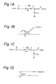
- a sample and hold circuit (hereinafter referred to as a S/H circuit) is comprised of a sampling switch and a holding capacitor. One end of the switch is connected to an input terminal of the circuit and another end of the switch is connected to an output terminal of the circuit as well as to the capacitor.
- An analogue signal is applied to the input terminal: When the switch is turned on, the capacitor is charged, i.e., a sampling is effected. After the sampling, the voltage is held even when the switch is turned off. Thus, the sampled voltage of an analogue signal is converted to a constantly held voltage. This technique is applied to, for example, an A/D converter.
- MOS transistor Metal Oxide Semiconductor
- the MOS transistor is comprised of a gate, a source, a drain and . bulk silicon under the gate.
- the drain (or source) is connected to the input terminal of the S/H circuit
- the source (or drain) is connected to the output terminal of the S/H circuit, as well as to the holding capacitor, and the gate is used as a switching terminal.
- the MOS transistor is switched from the on state to the off state or vice versa by changing a control voltage applied to the gate.
- the above-mentioned change of the output voltage is based on the following two reasons. The first reason is that the control voltage applied to the gate in the on state is different from the control voltage in the off state. The second reason is that a channel region formed between the source and the drain during the on state disappears in the off state.
- a dummy capacitor having the same capacity as a parasitic capacitor between the gate and the source in the MOS transistor.
- the dummy capacitor is connected, through an inverter, between the gate and the source outside the MOS transistor.
- the primary object of the present invention to provide a sample and hold circuit employing a first MOS transistor as a sampling switch wherein the output voltage is kept substantially constant before and after the MOS transistor is turned off.
- a sample-and-hold circuit has an input terminal, an output terminal, a first field-effect transistor for sampling . an input voltage applied to the input terminal, the first field-effect transistor being connected between the input terminal and the output terminal, a holding capacitor for holding the sampled input voltage, and a further capacitance connected to the output terminal and arranged to receive a voltage substantially equal and opposite in polarity to the voltage applied to the gate terminal of the first field-effect transistor and is characterised in that the said further capacitance is provided by a second field-effect transistor whose source and drain are commonly connected to the said output terminal, whose gate receives as a control voltage the said substantially equal and opposite voltage and which provides, between its base, on the one hand and its source and drain, on the other hand, a total capacitance which is substantially equal to the capacitance between the gate of the first field-effect transistor and the output electrode of the first field-effect transistor.
- This sample and hold circuit employs the second transistor as a dummy "capacitor" wherein a charge accumulation in the channel region of the first transistor can be absorbed.by the second transistor after the first transistor is turned off.
- the required capacitance values are obtained by arranging that the size of the second field-effect transistor is substantially half the size of the first field-effect transistor.
- the first field-effect transistor may comprise three diffusion regions as source or drain regions, the three diffusion regions being separated from each other by a constant distance for forming two channel regions, each of the channel regionsbeing formed between an adjacent two of the diffusion regions, with a gate electrode covering the two channel regions.
- the second field-effect transistor may comprise two diffusion regions as source and drain regions, and a gate electrode: covering a channel region between these two diffusion regions.
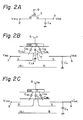
- F ig. 2B is a schematic structural diagram of the MOS transistor when it is in the on state.
- the MOS transistor in the on state is comprised of bulk silicon B, a source region S and a drain region D formed on the bulk silicon B, a channel region C between the source region S and the drain region D, an insulating layer of SiO 2 formed on the source, channel and drain regions, and a gate region G formed on the insulating layer.
- parasitic capacitors such as a capacitor C GS between the gate and the source, a capacitor C GD between the gate and the drain, a capacitor C GC between the gate and the channel, and a capacitor C CB between the channel and the bulk silicon.
- a voltage V of, for example, 5 V, for turning on the MOS transistor is applied to the switching terminal 6.
- Fig. 2C is a schematic structural diagram of the MOS transistor in the off state.
- the differences between Fig. 2B and Fig. 2C are that the channel region C in Fig. 2B has disappeared in Fig. 2C and the voltage applied to the switching terminal 6 is changed from V A to V B of, for example, minus 5 V, for turning off the MOS transistor. Because the channel region disappears in the off state, the capacitors C GC and C CB in Fig. 2B are replaced by a capacitor C GB between the gate and the bulk silicon.
- Fig. 2D is an equivalent circuit diagram of Fig. 2B
- Fig. 2E is an equivalent circuit diagram of Fig. 2C.
- the capacitor C GS among the parasitic capacitors is illustrated in Figs. 2D and 2E.
- the voltage V A for turning on the MOS transistor is applied to the switching input 6 and, therefore, the switch SW is turned on.
- the voltage V B for turning off the MOS transistor is applied to the control input 6 and thus the switch SW is turned off.
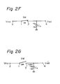
- Fig. 2F is another equivalent circuit diagram of Fig. 2B
- Fig. 2G is another equivalent circuit diagram of Fig. 2C.
- the parasitic capacitors C GS and C GD are not illustrated for the purpose of simplicity: When the MOS transistor is turned on, charges are stored between the gate and the channel, and between the channel and the bulk silicon. When the MOS transistor is turned off, the channel region disappears as described above (Fig. 2C). Therefore, a part of the stored charge flows into the source region and the drain region.
- FIG. 3A is the circuit diagram of this prior-art S/H circuit. As illustrated in Fig. 3A, a dummy capacitor 7 and an inverter 8 are connected in series between the gate and the source of the MOS transistor 5. The capacitance of the dummy capacitor 7 is the same as the parasitic capacitance C GS between the gate and the drain within the MOS transistor. The other construction is the same as the construction in the circuit of Fig. 2A.
- the voltage V A for turning on the MOS transistor 5 is applied to the gate of the MOS transistor, the voltage V A is inverted by the inverter 8 to the voltage V B which is applied to the dummy capacitor 7.
- the voltage V B for turning off the MOS transistor 5 is applied to the gate of the transistor 5, the voltage V B is inverted by the inverter 8 to the voltage V A which is applied to the dummy capacitor 7.
- Fig. 3B is an equivalent circuit diagram of Fig. 3A when the voltage V A is applied to the gate of the transistor 5.
- the voltage applied to the dummy capacitor 7 is equal to V B , as mentioned above.
- the switch SW in Fig. 3B is turned on because the voltage.V A for turning on the MOS transistor 5 is applied to the gate of the MOS transistor 5. Let it be assumed that, in this state, the amount of charge stored in the parasitic capacitor C GS is Q A and the amount of charge stored in the dummy capacitor 7 is Q B .
- Fig. 3C is an equivalent circuit diagram of Fig. 3A when the voltage V B is applied to the gate of the transistor 5.
- the voltage applied to the dummy capacitor 7 in this case is equal to V A .
- the switch SW in Fig. 3C is turned off because the voltage V B for turning off the MOS transistor 5 is applied to the gate of the MOS transistor 5. Since the parasitic capacitance C GS is equal to the capacitance of the dummy capacitor 7, the amount of charge stored in the parasitic capacitor C GS is Q B and the amount of charge stored in the dummy capacitor 7 is Q A as indicated in Fig. 3C.
- the output voltage V out in Fig. 3B is, in theory, equal to the output voltage V' out in Fig. 3C with respect to the variation of the control voltage.
- the values of the parasitic capacitances C GS in various MOS transistors are not usually the same, because the values of the parasitic capacitances vary depending on the manufacturing conditions.
- the dummy capacitor 7 is fabricated independent of the fabrication of the MOS transistor 5, it is difficult to fabricate the dummy capacitor 7 so that it has the same capacitance as the parasitic capacitor C GS in the MOS transistor 5. Accordingly, the output voltage V' out in the off state is, in practice, usually different from the output voltage V out in the on state.
- Fig. 4B is an equivalent circuit diagram of Fig. 4A when a voltage V A of, for example, plus 5 volts is applied to the switching terminal 6.
- the first MOS transistor 5 is comprised of a first switch SW1 and the capacitor C GS connected in series between the input terminal 2 and the switching terminal 6. Since the voltage V is applied to the gate of the MOS transistor 5, the switch SW1 is in the on state.
- the second MOS transistor 10 is comprised of a second switch SW2 and two capacitors C 11 and C 12 connected in parallel. These capacitors C 11 and C 12 are the capacitors between the gate and the source and between the gate and the drain, respectively, each having a half capacitance of the capacitor C GS of the first MOS transistor 5.
- the second switch SW2 is connected between the capacitors C 11 and C 12 .
- the connecting point between the capacitor C12 and the second switch SW2 is connected to the connecting point between the first switch SW1 and the capacitor C GS .
- the other end of the second switch SW2 is connected to the output terminal 4.
- the holding capacitor C o is connected between the output terminal 4 and the ground. Since the voltage applied to the gate of the second MOS transistor 10 is V B of, for example, minus 5 volts, the second switch SW2 is in the off state. In this condition, let it be assumed that the amount of charge stored in the capacitor C GS is Q A and the amount of charge stored in each of the capacitors C 11 and C 12 is Q B /2. The voltage applied to the switching terminal 6 is then changed from V A to V B for holding the sampled voltage V ino .
- the charges which have flowed out from the capacitor C GS are completely absorbed by the two capacitors C 11 and 12 .
- the second MOS transistor 10 (Fig. 4A) is turned on in this condition, the amount of charges ⁇ Q 0 which have flowed out from the channel region of the first MOS transistor 5 is completely absorbed by the channel region of the second MOS transistor 10. Consequently, no charge flows into the holding capacitor C 0 by varying the control voltage from V A to V B .
- the output voltage V' out after turning off the first MOS transistor 5 is equal to the output voltage V out before turning off the first MOS transistor 5.
- Fig. 5A illustrates a plan view of the sample and hold circuit according to the above-mentioned embodiment of the present invention.
- the first MOS transistor 5 is comprised of two drain regions 22 and 24, one source region 26, and one gate region 28.
- the second MOS transistor 10 is comprised of one drain region 32, one source region 34 and one gate region 36.
- the distance from a drain region to a neighbouring source region is constant for all cases and is denoted by "L”.
- the width of each drain region or source region is constant and is represented by "W”.
- two drain regions 22 and 24 are electrically connected by means of aluminum wiring, polysilicon wiring, etc.
- the capacitor between the gate and the * source of the first MOS transistor 5 is represented in Fig.
- Fig. 5B is a plan view of the S/H circuit when the gate regions 28 and 36 are shifted to the left by the distance L 0 from the positions of the gate regions in Fig. 5A.
- the wiring is not illustrated in Fig. 5B for the purpose of simplification. Since the gate region 28 is shifted by the same amount as the shift of the gate region 36, the amount of decrease in the area Al is the same as the amount of decrease in the area B2, and the amount of increase in the area A2 is the same as the amount of increase in the area Bl. Therefore, inspite of shifting the gate regions, the above formula (2) is satisfied.
- the mask is not restricted to the one for forming the gate regions, but alternatively, may be the one for forming a wiring pattern, and drain and source regions. In all of these cases, the above formula (2) can be satisfied.
- Fig. 5C is a plan view of the S/H circuit of an embodiment when the area of the source and drain regions are increased in comparison with the source and drain regions in Fig. 5A, even when the same mask is used in the circuits of Fig. 5A and Fig. 5C.
- the increase in the area of the source and the drain regions 22, 24, 26, 32 and 34 in the transverse direction by the same amount each of the areas Al, A2, Bl and B2 is increased by the same amount. Accordingly, the above formula (2) can be satisfied even when the area of the source and drain regions is increased; when the area of the source and drain regions is decreased, the formula (2) can also be satisfied.
Landscapes
- Electronic Switches (AREA)
- Measurement Of Current Or Voltage (AREA)
Applications Claiming Priority (2)
| Application Number | Priority Date | Filing Date | Title |
|---|---|---|---|
| JP6855279A JPS55163694A (en) | 1979-06-01 | 1979-06-01 | Sample holding circuit |
| JP68552/79 | 1979-06-01 |
Publications (2)
| Publication Number | Publication Date |
|---|---|
| EP0020160A1 true EP0020160A1 (fr) | 1980-12-10 |
| EP0020160B1 EP0020160B1 (fr) | 1982-12-22 |
Family
ID=13377031
Family Applications (1)
| Application Number | Title | Priority Date | Filing Date |
|---|---|---|---|
| EP80301802A Expired EP0020160B1 (fr) | 1979-06-01 | 1980-05-30 | Circuit d'échantillonnage et de mémorisation |
Country Status (4)
| Country | Link |
|---|---|
| US (1) | US4393318A (fr) |
| EP (1) | EP0020160B1 (fr) |
| JP (1) | JPS55163694A (fr) |
| DE (1) | DE3061413D1 (fr) |
Cited By (7)
| Publication number | Priority date | Publication date | Assignee | Title |
|---|---|---|---|---|
| EP0308007A3 (en) * | 1987-09-16 | 1990-09-05 | Philips Electronic And Associated Industries Limited | A circuit arrangement for storing sampled analogue electrical currents |
| EP0345156A3 (en) * | 1988-05-31 | 1990-10-17 | Fujitsu Limited | Analog switch circuit |
| US5084634A (en) * | 1990-10-24 | 1992-01-28 | Burr-Brown Corporation | Dynamic input sampling switch for CDACS |
| US5162670A (en) * | 1990-01-26 | 1992-11-10 | Kabushiki Kaisha Toshiba | Sample-and-hold circuit device |
| GB2270431A (en) * | 1992-09-08 | 1994-03-09 | Fujitsu Ltd | Voltage storage circuits |
| EP0597200A1 (fr) * | 1992-11-10 | 1994-05-18 | Fraunhofer-Gesellschaft Zur Förderung Der Angewandten Forschung E.V. | Commutateur analogique avec FET-AsGa |
| EP0917289A2 (fr) * | 1997-11-17 | 1999-05-19 | STMicroelectronics GmbH | Circuit intégré à capacité commutée |
Families Citing this family (18)
| Publication number | Priority date | Publication date | Assignee | Title |
|---|---|---|---|---|
| US4467227A (en) * | 1981-10-29 | 1984-08-21 | Hughes Aircraft Company | Channel charge compensation switch with first order process independence |
| JPS5894232A (ja) * | 1981-11-30 | 1983-06-04 | Toshiba Corp | 半導体アナログスイッチ回路 |
| US4499387A (en) * | 1981-12-15 | 1985-02-12 | Tokyo Shibaura Denki Kabushiki Kaisha | Integrated circuit formed on a semiconductor substrate with a variable capacitor circuit |
| US4500800A (en) * | 1982-08-30 | 1985-02-19 | International Business Machines Corporation | Logic performing cell for use in array structures |
| JPS5994923A (ja) * | 1982-11-22 | 1984-05-31 | Toshiba Corp | アナログ・スイツチ回路 |
| US4508983A (en) * | 1983-02-10 | 1985-04-02 | Motorola, Inc. | MOS Analog switch driven by complementary, minimally skewed clock signals |
| US4651037A (en) * | 1983-06-07 | 1987-03-17 | Nec Corporation | Precision analog switching circuit employing MOS transistors |
| US5164616A (en) * | 1989-12-29 | 1992-11-17 | Xerox Corporation | Integrated sample and hold circuit with feedback circuit to increase storage time |
| US5187390A (en) * | 1991-07-12 | 1993-02-16 | Crystal Semiconductor Corporation | Input sampling switch charge conservation |
| US5457415A (en) * | 1992-10-30 | 1995-10-10 | International Business Machines Corporation | Charge metering sampling circuit and use thereof in TFT/LCD |
| JP2000505927A (ja) * | 1996-01-31 | 2000-05-16 | アナロジック コーポレーション | リセット電荷補償回路 |
| EP1007983A4 (fr) | 1997-03-13 | 2000-07-12 | Wavecrest Corp | Analyse de bruit dans des formes d'ondes repetitives |
| US6323696B1 (en) | 1999-12-07 | 2001-11-27 | Hughes Electronics Corporation | Sample and hold circuit |
| US6781434B2 (en) * | 2000-12-28 | 2004-08-24 | Intel Corporation | Low charge-dump transistor switch |
| GB0416803D0 (en) * | 2004-07-27 | 2004-09-01 | Wood John | Rotary flash ADC |
| CN100442662C (zh) * | 2005-12-16 | 2008-12-10 | 威盛电子股份有限公司 | 传输电路及相关方法 |
| US7834665B2 (en) * | 2007-10-17 | 2010-11-16 | Agilent Technologies, Inc. | Track-and-hold circuit with adjustable charge compensation |
| FR3098363A1 (fr) * | 2019-07-04 | 2021-01-08 | Stmicroelectronics Sa | Circuit échantillonneur |
Citations (5)
| Publication number | Priority date | Publication date | Assignee | Title |
|---|---|---|---|---|
| DE1270171B (de) * | 1960-10-31 | 1968-06-12 | Asea Ab | Fremdgesteuerte Abtastschaltung zur periodischen Messung einer zeitlich sich aendernden Spannung |
| GB1413036A (en) * | 1972-10-20 | 1975-11-05 | Westinghouse Electric Corp | Coherent sampled readout circuit and signal processor for a charge coupled device array |
| US4068136A (en) * | 1975-10-13 | 1978-01-10 | Matsushita Electric Industrial Co., Ltd. | Analog voltage memory device |
| DE2704483A1 (de) * | 1977-02-03 | 1978-08-10 | Bosch Gmbh Robert | Schaltungsanordnung zum zeitselektiven abtasten und speichern |
| DE2718175A1 (de) * | 1977-04-23 | 1978-11-02 | Licentia Gmbh | Abtast-halte-schaltung |
Family Cites Families (9)
| Publication number | Priority date | Publication date | Assignee | Title |
|---|---|---|---|---|
| US3586880A (en) * | 1969-08-11 | 1971-06-22 | Astrodata Inc | Isolation and compensation of sample and hold circuits |
| US3594589A (en) * | 1970-03-23 | 1971-07-20 | Massachusetts Inst Technology | Sample and hold circuit |
| US3764921A (en) * | 1972-10-27 | 1973-10-09 | Control Data Corp | Sample and hold circuit |
| JPS5152755A (fr) * | 1974-11-05 | 1976-05-10 | Hitachi Ltd | |
| JPS5222871A (en) * | 1975-08-14 | 1977-02-21 | Fujitsu Ltd | Sampler circuit |
| US4048525A (en) * | 1975-09-02 | 1977-09-13 | General Electric Company | Output circuit for charge transfer transversal filter |
| US4010388A (en) * | 1976-02-18 | 1977-03-01 | Teletype Corporation | Low power asynchronous latch |
| JPS5355935A (en) * | 1976-10-30 | 1978-05-20 | Oki Electric Ind Co Ltd | Sample holding circuit |
| US4176289A (en) * | 1978-06-23 | 1979-11-27 | Electronic Memories & Magnetics Corporation | Driving circuit for integrated circuit semiconductor memory |
-
1979
- 1979-06-01 JP JP6855279A patent/JPS55163694A/ja active Granted
-
1980
- 1980-05-30 EP EP80301802A patent/EP0020160B1/fr not_active Expired
- 1980-05-30 US US06/154,949 patent/US4393318A/en not_active Expired - Lifetime
- 1980-05-30 DE DE8080301802T patent/DE3061413D1/de not_active Expired
Patent Citations (5)
| Publication number | Priority date | Publication date | Assignee | Title |
|---|---|---|---|---|
| DE1270171B (de) * | 1960-10-31 | 1968-06-12 | Asea Ab | Fremdgesteuerte Abtastschaltung zur periodischen Messung einer zeitlich sich aendernden Spannung |
| GB1413036A (en) * | 1972-10-20 | 1975-11-05 | Westinghouse Electric Corp | Coherent sampled readout circuit and signal processor for a charge coupled device array |
| US4068136A (en) * | 1975-10-13 | 1978-01-10 | Matsushita Electric Industrial Co., Ltd. | Analog voltage memory device |
| DE2704483A1 (de) * | 1977-02-03 | 1978-08-10 | Bosch Gmbh Robert | Schaltungsanordnung zum zeitselektiven abtasten und speichern |
| DE2718175A1 (de) * | 1977-04-23 | 1978-11-02 | Licentia Gmbh | Abtast-halte-schaltung |
Cited By (11)
| Publication number | Priority date | Publication date | Assignee | Title |
|---|---|---|---|---|
| EP0308007A3 (en) * | 1987-09-16 | 1990-09-05 | Philips Electronic And Associated Industries Limited | A circuit arrangement for storing sampled analogue electrical currents |
| EP0345156A3 (en) * | 1988-05-31 | 1990-10-17 | Fujitsu Limited | Analog switch circuit |
| US5019731A (en) * | 1988-05-31 | 1991-05-28 | Fujitsu Limited | Analog switch circuit |
| US5162670A (en) * | 1990-01-26 | 1992-11-10 | Kabushiki Kaisha Toshiba | Sample-and-hold circuit device |
| US5084634A (en) * | 1990-10-24 | 1992-01-28 | Burr-Brown Corporation | Dynamic input sampling switch for CDACS |
| GB2270431A (en) * | 1992-09-08 | 1994-03-09 | Fujitsu Ltd | Voltage storage circuits |
| US5384570A (en) * | 1992-09-08 | 1995-01-24 | Fujitsu Limited | Voltage storage circuits |
| GB2270431B (en) * | 1992-09-08 | 1997-03-26 | Fujitsu Ltd | Voltage summation circuitry, voltage doubling circuitry and analog-to-digital converters employing such circuitry |
| USRE36014E (en) * | 1992-09-08 | 1998-12-29 | Fujitsu Limited | Voltage storage circuits |
| EP0597200A1 (fr) * | 1992-11-10 | 1994-05-18 | Fraunhofer-Gesellschaft Zur Förderung Der Angewandten Forschung E.V. | Commutateur analogique avec FET-AsGa |
| EP0917289A2 (fr) * | 1997-11-17 | 1999-05-19 | STMicroelectronics GmbH | Circuit intégré à capacité commutée |
Also Published As
| Publication number | Publication date |
|---|---|
| DE3061413D1 (en) | 1983-01-27 |
| EP0020160B1 (fr) | 1982-12-22 |
| US4393318A (en) | 1983-07-12 |
| JPS5653839B2 (fr) | 1981-12-22 |
| JPS55163694A (en) | 1980-12-19 |
Similar Documents
| Publication | Publication Date | Title |
|---|---|---|
| EP0020160B1 (fr) | Circuit d'échantillonnage et de mémorisation | |
| US4511814A (en) | Semiconductor analog switch circuit with compensation means to minimize offset of output voltage | |
| US6693316B2 (en) | Semiconductor apparatus having a charge pump circuit | |
| US4945067A (en) | Intra-gate offset high voltage thin film transistor with misalignment immunity and method of its fabrication | |
| US4071775A (en) | Charge coupled differential amplifier for transversal filter | |
| EP0191587B1 (fr) | Dispositifs à transfert de charges | |
| US4616249A (en) | Solid state image pick-up element of static induction transistor type | |
| US4627082A (en) | Semiconductor device for obtaining an accurate threshold voltage adjustment | |
| US4132903A (en) | CCD output circuit using thin film transistor | |
| US4251829A (en) | Insulated gate field-effect transistor | |
| US3790825A (en) | Gate-diffusion isolation for jfet depletion-mode bucket brigade circuit | |
| US4695715A (en) | Infrared imaging array employing metal tabs as connecting means | |
| US4709380A (en) | Bucket brigade charge transfer device with auxiliary gate electrode | |
| US4144526A (en) | Circuit arrangement and operating process for converting an analogue signal into a digital signal | |
| US4103333A (en) | Charge coupled correlator device | |
| US4124861A (en) | Charge transfer filter | |
| US4374334A (en) | Signal comparator apparatus | |
| KR100249412B1 (ko) | 전하 결합 장치 | |
| JPS6111009B2 (fr) | ||
| US4255673A (en) | Input charge corrected monolithically integrated charge transfer device (CTD) arrangement | |
| US5087843A (en) | Input circuit for ccd delay line | |
| US3987475A (en) | Nondestructive charge sensing in a charge coupled device | |
| US5204989A (en) | Charge sensing device | |
| US4539537A (en) | Transversal filter having parallel inputs | |
| EP0046549B1 (fr) | Etage de sortie d'un dispositif à transfert de charges monolithiquement intégré |
Legal Events
| Date | Code | Title | Description |
|---|---|---|---|
| PUAI | Public reference made under article 153(3) epc to a published international application that has entered the european phase |
Free format text: ORIGINAL CODE: 0009012 |
|
| 17P | Request for examination filed | ||
| AK | Designated contracting states |
Designated state(s): DE FR GB NL |
|
| GRAA | (expected) grant |
Free format text: ORIGINAL CODE: 0009210 |
|
| AK | Designated contracting states |
Designated state(s): DE FR GB NL |
|
| REF | Corresponds to: |
Ref document number: 3061413 Country of ref document: DE Date of ref document: 19830127 |
|
| ET | Fr: translation filed | ||
| PLBI | Opposition filed |
Free format text: ORIGINAL CODE: 0009260 |
|
| 26 | Opposition filed |
Opponent name: SIEMENS AG, BERLIN UND MUENCHEN Effective date: 19830216 |
|
| PLBI | Opposition filed |
Free format text: ORIGINAL CODE: 0009260 |
|
| 26 | Opposition filed |
Opponent name: DEUTSCHE ITT INDUSTRIES GMBH Effective date: 19830611 |
|
| PGFP | Annual fee paid to national office [announced via postgrant information from national office to epo] |
Ref country code: FR Payment date: 19840402 Year of fee payment: 5 |
|
| PGFP | Annual fee paid to national office [announced via postgrant information from national office to epo] |
Ref country code: DE Payment date: 19840727 Year of fee payment: 5 |
|
| PGFP | Annual fee paid to national office [announced via postgrant information from national office to epo] |
Ref country code: NL Payment date: 19850531 Year of fee payment: 6 |
|
| RDAG | Patent revoked |
Free format text: ORIGINAL CODE: 0009271 |
|
| STAA | Information on the status of an ep patent application or granted ep patent |
Free format text: STATUS: PATENT REVOKED |
|
| 27W | Patent revoked |
Effective date: 19860209 |
|
| NLR2 | Nl: decision of opposition | ||
| GBPC | Gb: european patent ceased through non-payment of renewal fee | ||
| REG | Reference to a national code |
Ref country code: FR Ref legal event code: ST |