EP0020164B1 - Monolithische Matrix mit Hochspannungs-MOS-Transistoren - Google Patents
Monolithische Matrix mit Hochspannungs-MOS-Transistoren Download PDFInfo
- Publication number
- EP0020164B1 EP0020164B1 EP80301808A EP80301808A EP0020164B1 EP 0020164 B1 EP0020164 B1 EP 0020164B1 EP 80301808 A EP80301808 A EP 80301808A EP 80301808 A EP80301808 A EP 80301808A EP 0020164 B1 EP0020164 B1 EP 0020164B1
- Authority
- EP
- European Patent Office
- Prior art keywords
- hvmosfet
- field plate
- drain
- substrate
- field
- Prior art date
- Legal status (The legal status is an assumption and is not a legal conclusion. Google has not performed a legal analysis and makes no representation as to the accuracy of the status listed.)
- Expired
Links
Images


Classifications
-
- H—ELECTRICITY
- H10—SEMICONDUCTOR DEVICES; ELECTRIC SOLID-STATE DEVICES NOT OTHERWISE PROVIDED FOR
- H10D—INORGANIC ELECTRIC SEMICONDUCTOR DEVICES
- H10D64/00—Electrodes of devices having potential barriers
- H10D64/111—Field plates
-
- H—ELECTRICITY
- H10—SEMICONDUCTOR DEVICES; ELECTRIC SOLID-STATE DEVICES NOT OTHERWISE PROVIDED FOR
- H10D—INORGANIC ELECTRIC SEMICONDUCTOR DEVICES
- H10D30/00—Field-effect transistors [FET]
- H10D30/60—Insulated-gate field-effect transistors [IGFET]
- H10D30/601—Insulated-gate field-effect transistors [IGFET] having lightly-doped drain or source extensions, e.g. LDD IGFETs or DDD IGFETs
- H10D30/603—Insulated-gate field-effect transistors [IGFET] having lightly-doped drain or source extensions, e.g. LDD IGFETs or DDD IGFETs having asymmetry in the channel direction, e.g. lateral high-voltage MISFETs having drain offset region or extended drain IGFETs [EDMOS]
-
- H—ELECTRICITY
- H10—SEMICONDUCTOR DEVICES; ELECTRIC SOLID-STATE DEVICES NOT OTHERWISE PROVIDED FOR
- H10D—INORGANIC ELECTRIC SEMICONDUCTOR DEVICES
- H10D30/00—Field-effect transistors [FET]
- H10D30/60—Insulated-gate field-effect transistors [IGFET]
- H10D30/611—Insulated-gate field-effect transistors [IGFET] having multiple independently-addressable gate electrodes influencing the same channel
-
- H—ELECTRICITY
- H10—SEMICONDUCTOR DEVICES; ELECTRIC SOLID-STATE DEVICES NOT OTHERWISE PROVIDED FOR
- H10D—INORGANIC ELECTRIC SEMICONDUCTOR DEVICES
- H10D62/00—Semiconductor bodies, or regions thereof, of devices having potential barriers
- H10D62/10—Shapes, relative sizes or dispositions of the regions of the semiconductor bodies; Shapes of the semiconductor bodies
- H10D62/17—Semiconductor regions connected to electrodes not carrying current to be rectified, amplified or switched, e.g. channel regions
- H10D62/213—Channel regions of field-effect devices
- H10D62/221—Channel regions of field-effect devices of FETs
- H10D62/235—Channel regions of field-effect devices of FETs of IGFETs
- H10D62/299—Channel regions of field-effect devices of FETs of IGFETs having lateral doping variations
- H10D62/307—Channel regions of field-effect devices of FETs of IGFETs having lateral doping variations the doping variations being parallel to the channel lengths
-
- H—ELECTRICITY
- H10—SEMICONDUCTOR DEVICES; ELECTRIC SOLID-STATE DEVICES NOT OTHERWISE PROVIDED FOR
- H10D—INORGANIC ELECTRIC SEMICONDUCTOR DEVICES
- H10D64/00—Electrodes of devices having potential barriers
- H10D64/111—Field plates
- H10D64/115—Resistive field plates, e.g. semi-insulating field plates
-
- H—ELECTRICITY
- H10—SEMICONDUCTOR DEVICES; ELECTRIC SOLID-STATE DEVICES NOT OTHERWISE PROVIDED FOR
- H10D—INORGANIC ELECTRIC SEMICONDUCTOR DEVICES
- H10D64/00—Electrodes of devices having potential barriers
- H10D64/60—Electrodes characterised by their materials
- H10D64/605—Source, drain, or gate electrodes for FETs comprising highly resistive materials
Definitions
- This invention relates to a high voltage metal oxide semiconductor field effect transistor (HVMOSFET) according to the first part of claim 1.
- HVMOSFET high voltage metal oxide semiconductor field effect transistor
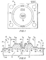
- a substrate 15 has an annulus 55 of metal oxide deposited on drift area 51, the inner part of the annulus being significantly thicker than the outer part 50.
- Two annular gate electrodes 70 and 80, with their respective leads 75 and 85, are deposited on the stepped surface of the oxide 55, with electrode 80 being for high voltage and electrode 70 for low voltage.
- the central drain electrode 40, with its lead 45, makes conductive contact with an N-doped region 35 of the substrate 15.
- the floating field plate 81 may be a lipped annulus in configuration, thereby allowing tunnelling to occur at the drain area 35 and not over the junction 100 or the drift region 51. As the floating field plate gets further from the drain area 35, the oxide 55 underneath has to support a relatively higher field in the "off" condition of the device 10.
- a slightly conductive layer such as a floating field plate 81
- a slightly conductive layer can replace the oxide 55, using SiO z or S '3 N 4 , over the junction 100 and drift region 51.
- the plate 81 may be a semi-insulating polysilicon SiPOS such as oxygen doped polysilicon.
- the oxygen doped poly for the plate 81 can be put in direct contact with the surface 65 of the P-silicon substrate 15 or alternatively over a relatively thin oxide (not shown). Because of the plate's finite though relatively low conductivity, it may act as a very high resistance field plate 81, thereby avoiding the problem of hot electron injection and trapping in the oxide 55 near the drain area 35 as mentioned above.
Landscapes
- Insulated Gate Type Field-Effect Transistor (AREA)
Claims (13)
Applications Claiming Priority (4)
| Application Number | Priority Date | Filing Date | Title |
|---|---|---|---|
| US43563 | 1979-05-30 | ||
| US06/043,563 US4288801A (en) | 1979-05-30 | 1979-05-30 | Monolithic HVMOSFET active switch array |
| US4328379A | 1979-07-12 | 1979-07-12 | |
| US43283 | 1979-07-12 |
Publications (2)
| Publication Number | Publication Date |
|---|---|
| EP0020164A1 EP0020164A1 (de) | 1980-12-10 |
| EP0020164B1 true EP0020164B1 (de) | 1983-05-11 |
Family
ID=26720242
Family Applications (1)
| Application Number | Title | Priority Date | Filing Date |
|---|---|---|---|
| EP80301808A Expired EP0020164B1 (de) | 1979-05-30 | 1980-05-30 | Monolithische Matrix mit Hochspannungs-MOS-Transistoren |
Country Status (2)
| Country | Link |
|---|---|
| EP (1) | EP0020164B1 (de) |
| DE (1) | DE3063085D1 (de) |
Cited By (1)
| Publication number | Priority date | Publication date | Assignee | Title |
|---|---|---|---|---|
| US7995081B2 (en) | 2008-06-25 | 2011-08-09 | Palo Alto Research Center Incorporated | Anisotropically conductive backside addressable imaging belt for use with contact electrography |
Families Citing this family (15)
| Publication number | Priority date | Publication date | Assignee | Title |
|---|---|---|---|---|
| US4651186A (en) * | 1981-11-18 | 1987-03-17 | Mitsubishi Denki Kabushiki Kaisha | Field effect transistor with improved withstand voltage characteristic |
| FR2571178B1 (fr) * | 1984-09-28 | 1986-11-21 | Thomson Csf | Structure de circuit integre comportant des transistors cmos a tenue en tension elevee, et son procede de fabrication |
| GB2173037A (en) * | 1985-03-29 | 1986-10-01 | Philips Electronic Associated | Semiconductor devices employing conductivity modulation |
| EP0211972A1 (de) * | 1985-08-07 | 1987-03-04 | Eaton Corporation | EFET mit erhöhter Torelektrode |
| JP2530033B2 (ja) * | 1990-02-08 | 1996-09-04 | 株式会社東芝 | 絶縁ゲ―ト型集積回路 |
| WO1996019833A1 (en) * | 1994-12-20 | 1996-06-27 | Francis John Clough | High voltage thin film semiconductor device |
| DE10047168A1 (de) | 2000-09-22 | 2002-04-18 | Eupec Gmbh & Co Kg | Steuerbares Halbleiterbauelement |
| US6468878B1 (en) | 2001-02-27 | 2002-10-22 | Koninklijke Philips Electronics N.V. | SOI LDMOS structure with improved switching characteristics |
| US6717214B2 (en) | 2002-05-21 | 2004-04-06 | Koninklijke Philips Electronics N.V. | SOI-LDMOS device with integral voltage sense electrodes |
| US7368777B2 (en) | 2003-12-30 | 2008-05-06 | Fairchild Semiconductor Corporation | Accumulation device with charge balance structure and method of forming the same |
| US8080848B2 (en) | 2006-05-11 | 2011-12-20 | Fairchild Semiconductor Corporation | High voltage semiconductor device with lateral series capacitive structure |
| US8193565B2 (en) | 2008-04-18 | 2012-06-05 | Fairchild Semiconductor Corporation | Multi-level lateral floating coupled capacitor transistor structures |
| US8624302B2 (en) | 2010-02-05 | 2014-01-07 | Fairchild Semiconductor Corporation | Structure and method for post oxidation silicon trench bottom shaping |
| CN110473908B (zh) * | 2019-08-29 | 2023-01-17 | 杭州电子科技大学温州研究院有限公司 | 一种具有梯形氧化槽的绝缘层上硅ldmos晶体管 |
| CN113097306B (zh) * | 2021-03-27 | 2023-05-30 | 长江存储科技有限责任公司 | Mos器件及其制造方法、以及esd防护电路 |
Family Cites Families (5)
| Publication number | Priority date | Publication date | Assignee | Title |
|---|---|---|---|---|
| US3339128A (en) * | 1964-07-31 | 1967-08-29 | Rca Corp | Insulated offset gate field effect transistor |
| DE2250613A1 (de) * | 1972-10-16 | 1974-04-25 | Itt Ind Gmbh Deutsche | Isolierschicht-feldeffekttransistor |
| DE2706623A1 (de) * | 1977-02-16 | 1978-08-17 | Siemens Ag | Mis-fet fuer hohe source-drain-spannungen |
| DE2740702A1 (de) * | 1977-09-09 | 1979-03-22 | Siemens Ag | Feldeffekt-schalttransistor fuer hohe spannungen |
| GB2011178B (en) * | 1977-12-15 | 1982-03-17 | Philips Electronic Associated | Fieldeffect devices |
-
1980
- 1980-05-30 DE DE8080301808T patent/DE3063085D1/de not_active Expired
- 1980-05-30 EP EP80301808A patent/EP0020164B1/de not_active Expired
Cited By (1)
| Publication number | Priority date | Publication date | Assignee | Title |
|---|---|---|---|---|
| US7995081B2 (en) | 2008-06-25 | 2011-08-09 | Palo Alto Research Center Incorporated | Anisotropically conductive backside addressable imaging belt for use with contact electrography |
Also Published As
| Publication number | Publication date |
|---|---|
| EP0020164A1 (de) | 1980-12-10 |
| DE3063085D1 (en) | 1983-06-16 |
Similar Documents
| Publication | Publication Date | Title |
|---|---|---|
| EP0020164B1 (de) | Monolithische Matrix mit Hochspannungs-MOS-Transistoren | |
| US5517051A (en) | Silicon controlled rectifier structure for electrostatic discharge protection | |
| JP4006398B2 (ja) | 静電放電保護デバイスを有する集積回路 | |
| EP0032018B1 (de) | Integrierte Halbleiter-Schaltungsvorrichtung | |
| US5557127A (en) | Termination structure for mosgated device with reduced mask count and process for its manufacture | |
| US4586064A (en) | DMOS with high-resistivity gate electrode | |
| USRE33209E (en) | Monolithic semiconductor switching device | |
| US4860072A (en) | Monolithic semiconductor device and method of manufacturing same | |
| US4284997A (en) | Static induction transistor and its applied devices | |
| US4198648A (en) | Integrated semiconductor device | |
| US5043781A (en) | Semiconductor device | |
| JP2982785B2 (ja) | デプレッション型mos半導体素子およびmosパワーic | |
| US4786956A (en) | Input protection device for integrated circuits | |
| US5434445A (en) | Junction-isolated high-voltage MOS integrated device | |
| EP0582710A4 (de) | Elektrisch programmierbare speicherzelle. | |
| US5227655A (en) | Field effect transistor capable of easily adjusting switching speed thereof | |
| US5498899A (en) | Spiral resistor integrated on a semiconductor substrate | |
| US5072271A (en) | Protection circuit for use in semiconductor integrated circuit device | |
| EP0205203B1 (de) | Ladungsverschiebeanordnung | |
| US4684967A (en) | Low capacitance transistor cell element and transistor array | |
| US4969020A (en) | Semiconductor device | |
| KR900004726B1 (ko) | 대규모 집적회로용 보호회로 | |
| US4672402A (en) | Semiconductor circuit device including an overvoltage protection element | |
| US4063273A (en) | Fundamental logic circuit | |
| US4969024A (en) | Metal-oxide-semiconductor device |
Legal Events
| Date | Code | Title | Description |
|---|---|---|---|
| PUAI | Public reference made under article 153(3) epc to a published international application that has entered the european phase |
Free format text: ORIGINAL CODE: 0009012 |
|
| AK | Designated contracting states |
Designated state(s): DE FR |
|
| 17P | Request for examination filed |
Effective date: 19810509 |
|
| GRAA | (expected) grant |
Free format text: ORIGINAL CODE: 0009210 |
|
| AK | Designated contracting states |
Designated state(s): DE FR |
|
| REF | Corresponds to: |
Ref document number: 3063085 Country of ref document: DE Date of ref document: 19830616 |
|
| ET | Fr: translation filed | ||
| PGFP | Annual fee paid to national office [announced via postgrant information from national office to epo] |
Ref country code: FR Payment date: 19840301 Year of fee payment: 5 |
|
| PLBE | No opposition filed within time limit |
Free format text: ORIGINAL CODE: 0009261 |
|
| STAA | Information on the status of an ep patent application or granted ep patent |
Free format text: STATUS: NO OPPOSITION FILED WITHIN TIME LIMIT |
|
| 26N | No opposition filed | ||
| PG25 | Lapsed in a contracting state [announced via postgrant information from national office to epo] |
Ref country code: FR Free format text: LAPSE BECAUSE OF NON-PAYMENT OF DUE FEES Effective date: 19900131 |
|
| REG | Reference to a national code |
Ref country code: FR Ref legal event code: ST |
|
| PGFP | Annual fee paid to national office [announced via postgrant information from national office to epo] |
Ref country code: DE Payment date: 19970606 Year of fee payment: 18 |
|
| PG25 | Lapsed in a contracting state [announced via postgrant information from national office to epo] |
Ref country code: DE Free format text: LAPSE BECAUSE OF NON-PAYMENT OF DUE FEES Effective date: 19990302 |