EP0020185A1 - Verfahren und Vorrichtung zur seriell-parallelen Addition einer grossen Anzahl von Wörtern - Google Patents
Verfahren und Vorrichtung zur seriell-parallelen Addition einer grossen Anzahl von Wörtern Download PDFInfo
- Publication number
- EP0020185A1 EP0020185A1 EP80400354A EP80400354A EP0020185A1 EP 0020185 A1 EP0020185 A1 EP 0020185A1 EP 80400354 A EP80400354 A EP 80400354A EP 80400354 A EP80400354 A EP 80400354A EP 0020185 A1 EP0020185 A1 EP 0020185A1
- Authority
- EP
- European Patent Office
- Prior art keywords
- words
- binary
- transcoder
- weight
- adder
- Prior art date
- Legal status (The legal status is an assumption and is not a legal conclusion. Google has not performed a legal analysis and makes no representation as to the accuracy of the status listed.)
- Granted
Links
Images

Classifications
-
- G—PHYSICS
- G06—COMPUTING OR CALCULATING; COUNTING
- G06F—ELECTRIC DIGITAL DATA PROCESSING
- G06F7/00—Methods or arrangements for processing data by operating upon the order or content of the data handled
- G06F7/38—Methods or arrangements for performing computations using exclusively denominational number representation, e.g. using binary, ternary, decimal representation
- G06F7/48—Methods or arrangements for performing computations using exclusively denominational number representation, e.g. using binary, ternary, decimal representation using non-contact-making devices, e.g. tube, solid state device; using unspecified devices
- G06F7/50—Adding; Subtracting
- G06F7/504—Adding; Subtracting in bit-serial fashion, i.e. having a single digit-handling circuit treating all denominations after each other
- G06F7/5045—Adding; Subtracting in bit-serial fashion, i.e. having a single digit-handling circuit treating all denominations after each other for multiple operands
-
- G—PHYSICS
- G06—COMPUTING OR CALCULATING; COUNTING
- G06F—ELECTRIC DIGITAL DATA PROCESSING
- G06F7/00—Methods or arrangements for processing data by operating upon the order or content of the data handled
- G06F7/60—Methods or arrangements for performing computations using a digital non-denominational number representation, i.e. number representation without radix; Computing devices using combinations of denominational and non-denominational quantity representations, e.g. using difunction pulse trains, STEELE computers, phase computers
- G06F7/607—Methods or arrangements for performing computations using a digital non-denominational number representation, i.e. number representation without radix; Computing devices using combinations of denominational and non-denominational quantity representations, e.g. using difunction pulse trains, STEELE computers, phase computers number-of-ones counters, i.e. devices for counting the number of input lines set to ONE among a plurality of input lines, also called bit counters or parallel counters
Definitions
- the present invention relates to a method for rapidly processing binary words to perform simultaneous addition, and to a rapid adder device for implementing this method.
- the digital adders currently used to add several binary numbers, each having a large number of binary elements comprise a cascade of adding cells each carrying out two Boolean functions with three variables, the carry propagating from cell to cell, which requires a relatively long computation time.
- additional circuits are used which provide early restraint.
- the size of these latter adders becomes prohibitive when the format of the binary words to be added increases.
- the subject of the present invention is a method of processing binary words allowing the simultaneous addition of a large number of words composed of a large number of binary elements in the shortest possible time with the means currently available. , and also relates to an adder device for implementing this method.
- the processing method in accordance with the present invention consists, starting from words each stored in a shift register and extracted at the serial output of these registers, sequentially extracting all the binary elements of the same weight starting with those of most significant weight weak and progressing in order towards those of highest weight, to be determined at each times the number of "1" among all the binary elements of the same weight, to add, for each considered weight of binary elements, the number of "1" of retention relating to the binary elements of immediately lower weight, to calculate the half sum of these two numbers, to send a "1" in a shift register when this half-sum is not an integer, and a "0" otherwise, to memorize a number equal to the whole part of this half-sum, and extracting the latter number as a number of "1" holdbacks for use when calculating the immediately following half-sum.
- the device for implementing the method of the present invention comprises a transcoder device, the different inputs of which are connected to the serial outputs of the different shift registers in which the words to be added together are stored, this transcoder device being produced so as to present on its outputs the value, in pure binary, of the number of "1" present on its inputs, the outputs of this transcoder device being connected via a flip-flop register to corresponding binary weight inputs of a circuit parallel binary adder-divider itself connected to a storage register for the sum of the holdbacks, the least significant output of this adder-divider circuit being connected to the serial input of an output shift register.
- the transcoder device has a pyramid structure with several processing stages, the stage of input, at the base of the pyramid, comprising in parallel several elementary transcoder circuits each supplying on its different outputs the value, in pure binary, of the number of "1" for each binary weight of all the words arriving on all its inputs, the outputs of at least two different transcoder circuits being grouped, each time, at the input of an adder circuit presenting on its outputs the sum of the input values, several stages of such adder circuits being arranged in cascade, each of these stages comprising a number of adding circuits lower than that of the preceding stage, for example half, the last stage, at the top of the pyramid, comprising only one combinatory circuit.
- the different successive stages constituting the transcoder device are interconnected by means of flip-flop registers, with parallel inputs and outputs, all of the registers being connected to a common generator of clock
- the fast adder represented diagrammatically on the figurel is intended for the simultaneous addition of 127 words for example, each comprising a large number of binary elements, for example 32.
- 127 words for example, each comprising a large number of binary elements, for example 32.
- the number of words that the it can be added together may be different, and that the words may contain a different number of binary elements, the modifications to be made to the device of the invention being obvious to those skilled in the art on reading the presence description.
- the adder of FIG. 1 comprises, on the input side, p shift registers, respectively referenced 1 to 1 P , p being the number of words to be added together, 127 in the present case, these registers for example each comprising 32 cells if the maximum number n of binary elements of the words to be added is 32.
- the words to be added together can be introduced into these shift registers either in serial mode or in parallel mode depending on the configuration of the circuits connected upstream of the adder.
- each register 1 1 to 1 127 is connected to a corresponding input of a transcoder 2 described in more detail below.
- the transcoder 2 has seven outputs of respective binary weights 2 to 2.
- the different outputs of transcoder 2 are connected, through the intermediary diary of a register 3, to a series of corresponding inputs of the same weight of a binary adder-divider circuit 4 which can for example be produced in a manner known per se using two integrated circuits 74283 from Texas Instruments.
- Register 3 is with parallel inputs and outputs and is, for example, typically made up of eight D-type flip-flop cells, one of these cells being unused.
- the weakest point output of the adder-divider circuit 4 is connected to the serial input of a shift register 5 comprising a number of cells sufficient to contain all the binary elements of the result. For the aforementioned example of the addition of 127 words of 32 binary elements each, it is easily demonstrated that the result comprises a maximum of 39 binary elements.
- Register 5 will then be a standard 40 cell register.
- the other outputs of the adder-divider circuit 4 are respectively connected to another series of its corresponding weight inputs via a register 6 with parallel inputs and outputs, of the same constitution as register 3.
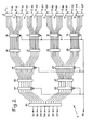
- FIG. 2 shows the detailed diagram of the transcoder device 2 in the case where 127 words of 32 binary elements each have to be added together.
- the transcoder 2 comprises, on the input side, a first stage with eight elementary transcoder circuits respectively referenced 8 to 15.
- These transcoder circuits for example FPLA (programmable logic networks) of the 82S100 type from Signetics with sixteen inputs, being programmed to supply each on its five outputs the value, in pure binary, of the total number of "1" present on all its inputs.
- the inputs of these transcoder circuits are respective ment referenced E 1 to E 127 , the last input of circuit 15 not being used.
- each time two transcoder circuits are grouped and connected, by means of flip-flop registers of type D, 16 to 19, to corresponding inputs of four adder circuits of a second processing stage, respectively referenced 20 to 23.
- Each of these four adder circuits provides the sum of its two input values from two corresponding transcoder circuits on its outputs.
- the outputs of the adder circuits 20 to 23 are also grouped for each time two adders and connected, via two registers 24 and 25, to corresponding inputs of two other adders 26, 27 forming the third processing stage, and finally the outputs of the adders 26 and 27 are connected via two registers 28, 29 to corresponding inputs of an adder 30 forming the last processing stage of the transcoder device and supplying the value on its seven outputs 31 to 37, pure binary, of the total of "1" of the same rank which were present simultaneously on the 127 inputs E to E 127 ,
- the clock signal inputs of all the registers are connected to a terminal 38 which is itself connected to terminal 7.
- the conformation of the transcoder device of FIG. 2 is due to the use of elementary trancoder circuits 8 to 15 with sixteen inputs each, the most efficient currently available, and that, of course, if transcoder circuits were available at 128 inputs, the device in FIG. 2 would be reduced to a single such circuit.
- the pyramidal structure in stages in accordance with the invention can still be used when it is desired to add together a number of words greater than the number of inputs of the available transcoder circuits.
- the outputs of the transcoder circuits and of the adder circuits can be grouped in a non-symmetrical manner, provided that the weights of the different outputs and inputs of the transcoder or adder circuits are respected.
- the different registers of the transcoder device 2 are not absolutely necessary, but it is preferable to use them. to properly synchronize the operation of the different stages of this transcoder device.
- the adder 30 On the second rising edge of the clock signal, the four partial sums supplied by the adders 20 to 23 arrive at the adders 26 and 27, the two partial sums of which reach the last adder 30 at the third rising edge of the clock signal, the adder 30 immediately providing to the input of register 3 the value in pure binary, the total of "1" of weight 2 0 words present in the input registers 1 1 to 1 127.
- Said first edge of the clock signal not only transfers into the adders 20 to 23 the results supplied by the transcoder circuits 8 to 15 for all the binary elements of weight 20 of the words to be added, but also presents the inputs E to E 127 binary elements of weight 2 1 which follow the same treatment as binary elements of weight 2 0 , and so on up to binary elements of weight 2 31
- the fourth rising edge of the clock signal transfers into the adder-divider 4 the first useful content of register 3, that is to say the value of the total of "1s" of weight 20 of the words to be added.
- the adder-divider 4 adds this value to the output value of register 6, which is zero because at the start of the addition of the words there is no reserve, register 6 having been previously reset so as to appropriate, then proceeds to a shift of one step to the right (towards the least significant binary elements) of this value, that is to say that it realizes the division by 2, then it sends in the register 5 the least significant binary element after shift, namely the fraction part nary (2) of the result of the division and sends to register 6 the other shifted bits.
- the adder 4 performs the half-sum of the value of the total of "1" of the binary weight considered and of the value of the total of "1" of carry, sends the fractional part of this half-sum in the register 5 and send the entire part to register 6 of deductions.
- the value of the total of the elements of binary weight 2 1 of the words to be added reaches the adder-divider 4 from the adder 3, and simultaneously, the register 6 sends it the value of the total deductions for binary items of weight 2 0 .
- the adder-divider 4 performs the sum of these two values, then divides it by two, sends the fractional part of the result in register 5 and the whole part in register 6.
Landscapes
- Engineering & Computer Science (AREA)
- General Physics & Mathematics (AREA)
- Physics & Mathematics (AREA)
- Theoretical Computer Science (AREA)
- Pure & Applied Mathematics (AREA)
- Computational Mathematics (AREA)
- Mathematical Analysis (AREA)
- Mathematical Optimization (AREA)
- General Engineering & Computer Science (AREA)
- Computing Systems (AREA)
- Mathematical Physics (AREA)
- Complex Calculations (AREA)
- Compression, Expansion, Code Conversion, And Decoders (AREA)
- Reduction Or Emphasis Of Bandwidth Of Signals (AREA)
Applications Claiming Priority (2)
| Application Number | Priority Date | Filing Date | Title |
|---|---|---|---|
| FR7909325A FR2454136B1 (fr) | 1979-04-12 | 1979-04-12 | Additionneur sequentiel rapide |
| FR7909325 | 1979-04-12 |
Publications (2)
| Publication Number | Publication Date |
|---|---|
| EP0020185A1 true EP0020185A1 (de) | 1980-12-10 |
| EP0020185B1 EP0020185B1 (de) | 1983-11-23 |
Family
ID=9224273
Family Applications (1)
| Application Number | Title | Priority Date | Filing Date |
|---|---|---|---|
| EP80400354A Expired EP0020185B1 (de) | 1979-04-12 | 1980-03-17 | Verfahren und Vorrichtung zur seriell-parallelen Addition einer grossen Anzahl von Wörtern |
Country Status (8)
| Country | Link |
|---|---|
| US (1) | US4336600A (de) |
| EP (1) | EP0020185B1 (de) |
| AU (1) | AU5737180A (de) |
| BR (1) | BR8002202A (de) |
| CA (1) | CA1158774A (de) |
| DE (1) | DE3065651D1 (de) |
| FR (1) | FR2454136B1 (de) |
| GR (1) | GR67742B (de) |
Cited By (4)
| Publication number | Priority date | Publication date | Assignee | Title |
|---|---|---|---|---|
| EP0375125A3 (de) * | 1988-12-23 | 1992-02-26 | Ampex Systems Corporation | Hochgeschwindiger digitaler Datenkorrelator mit einem synchronen Fliessbandfeld von Volladdiererzellen |
| GB2294138A (en) * | 1994-09-23 | 1996-04-17 | Cambridge Consultants | Data processing circuits and interfaces |
| US5978827A (en) * | 1995-04-11 | 1999-11-02 | Canon Kabushiki Kaisha | Arithmetic processing |
| US6311263B1 (en) | 1994-09-23 | 2001-10-30 | Cambridge Silicon Radio Limited | Data processing circuits and interfaces |
Families Citing this family (6)
| Publication number | Priority date | Publication date | Assignee | Title |
|---|---|---|---|---|
| EP0051079B1 (de) * | 1980-11-03 | 1984-09-26 | Deutsche ITT Industries GmbH | Binäres MOS-Ripple-Carry-Parallel-Addier/Subtrahierwerk und dafür geeignete Addier/Subtrahierstufe |
| EP0489952B1 (de) * | 1990-12-11 | 1998-08-19 | Siemens Aktiengesellschaft | Schaltungsanordnung zur digitalen Bit-seriellen Signalverarbeitung |
| US5361220A (en) * | 1991-11-29 | 1994-11-01 | Fuji Photo Film Co., Ltd. | Discrete cosine transformation with reduced components |
| EP0992882A3 (de) * | 1998-10-06 | 2003-03-05 | Texas Instruments Inc. | Bitfeldprozessor |
| US6760837B1 (en) | 1998-10-06 | 2004-07-06 | Texas Instruments Incorporated | Bit field processor |
| TWI444021B (zh) * | 2007-09-17 | 2014-07-01 | Htc Corp | 解譯串列傳輸訊號之方法 |
Citations (1)
| Publication number | Priority date | Publication date | Assignee | Title |
|---|---|---|---|---|
| US3636334A (en) * | 1969-01-02 | 1972-01-18 | Univ California | Parallel adder with distributed control to add a plurality of binary numbers |
Family Cites Families (3)
| Publication number | Priority date | Publication date | Assignee | Title |
|---|---|---|---|---|
| US3711692A (en) * | 1971-03-15 | 1973-01-16 | Goodyear Aerospace Corp | Determination of number of ones in a data field by addition |
| US3723715A (en) * | 1971-08-25 | 1973-03-27 | Ibm | Fast modulo threshold operator binary adder for multi-number additions |
| FR2212952A5 (de) * | 1972-12-29 | 1974-07-26 | Cit Alcatel |
-
1979
- 1979-04-12 FR FR7909325A patent/FR2454136B1/fr not_active Expired
-
1980
- 1980-03-17 DE DE8080400354T patent/DE3065651D1/de not_active Expired
- 1980-03-17 EP EP80400354A patent/EP0020185B1/de not_active Expired
- 1980-03-26 GR GR61527A patent/GR67742B/el unknown
- 1980-04-09 BR BR8002202A patent/BR8002202A/pt unknown
- 1980-04-10 CA CA000349541A patent/CA1158774A/en not_active Expired
- 1980-04-10 US US06/138,893 patent/US4336600A/en not_active Expired - Lifetime
- 1980-04-11 AU AU57371/80A patent/AU5737180A/en not_active Abandoned
Patent Citations (1)
| Publication number | Priority date | Publication date | Assignee | Title |
|---|---|---|---|---|
| US3636334A (en) * | 1969-01-02 | 1972-01-18 | Univ California | Parallel adder with distributed control to add a plurality of binary numbers |
Non-Patent Citations (1)
| Title |
|---|
| IEEE TRANSACTIONS ON COMPUTERS, Vol. C17, No. 10, Octobre 1968 New York (US) KOUVARAS et al.: "A Digital System of Simultaneous Addition of Several Binary Numbers", pages 992-997. * Figure 1; page 992, colonne de droite, alinea 2 a page 995, colonne de droite, alinea 5 * * |
Cited By (5)
| Publication number | Priority date | Publication date | Assignee | Title |
|---|---|---|---|---|
| EP0375125A3 (de) * | 1988-12-23 | 1992-02-26 | Ampex Systems Corporation | Hochgeschwindiger digitaler Datenkorrelator mit einem synchronen Fliessbandfeld von Volladdiererzellen |
| GB2294138A (en) * | 1994-09-23 | 1996-04-17 | Cambridge Consultants | Data processing circuits and interfaces |
| US6311263B1 (en) | 1994-09-23 | 2001-10-30 | Cambridge Silicon Radio Limited | Data processing circuits and interfaces |
| US6901503B2 (en) | 1994-09-23 | 2005-05-31 | Cambridge Consultants Ltd. | Data processing circuits and interfaces |
| US5978827A (en) * | 1995-04-11 | 1999-11-02 | Canon Kabushiki Kaisha | Arithmetic processing |
Also Published As
| Publication number | Publication date |
|---|---|
| GR67742B (de) | 1981-09-16 |
| US4336600A (en) | 1982-06-22 |
| DE3065651D1 (en) | 1983-12-29 |
| FR2454136A1 (fr) | 1980-11-07 |
| BR8002202A (pt) | 1980-11-25 |
| AU5737180A (en) | 1980-10-16 |
| CA1158774A (en) | 1983-12-13 |
| FR2454136B1 (fr) | 1985-12-06 |
| EP0020185B1 (de) | 1983-11-23 |
Similar Documents
| Publication | Publication Date | Title |
|---|---|---|
| EP0046708B1 (de) | Digitale Signalverarbeitungsschaltung in verteilter Arithmetik mit Verwendung eines Multiplexers am Eingang eines Speichers | |
| EP0198729B1 (de) | System zur Simulation einer elektronischen Schaltung | |
| EP0309037A1 (de) | Serieller Fliessband-Multiplizierer | |
| CH616252A5 (de) | ||
| EP0020185B1 (de) | Verfahren und Vorrichtung zur seriell-parallelen Addition einer grossen Anzahl von Wörtern | |
| EP0437876B1 (de) | Programmierbarer serieller Multiplikator | |
| FR2624282A1 (fr) | Comparateur binaire et operateur de tri de nombres binaires | |
| FR2480968A1 (fr) | Processeur numerique adapte a l'integration a haute densite | |
| FR2871976A1 (fr) | Decodeur ldpc | |
| FR3038188A1 (fr) | Systeme de verification de l’integrite d’une communication entre deux circuits | |
| EP0228528A1 (de) | Einrichtung zur Realisierung eines Kodes mit schwacher laufender Summe in schneller digitaler Übertragung und eine solche Einrichtung benutzendes Kodierungsverfahren | |
| FR2475250A1 (fr) | Multiplieur rapide | |
| EP0183610B1 (de) | Schreib-Lese-Speicher und Anwendung in einer linearen Interpolationsschaltung | |
| FR2773284A1 (fr) | Circuit de calcul de polynome de syndrome et un circuit de decodage reed-solomon | |
| EP0242258B1 (de) | Vorrichtung zur Durchführung eines Algorithmus (Leroux-Gueguen) zum Codieren eines Signals durch Linearvorhersage | |
| EP0215497A1 (de) | Autokorrelationseinrichtung | |
| EP0175623A1 (de) | Einrichtung zur Echtzeitdigitalsignalverarbeitung durch Faltung | |
| FR2731854A1 (fr) | Dispositif de filtrage digital | |
| EP0353826B1 (de) | Statistische Kodierungsvorrichtung zur Erzeugung von Kodewörtern mit einer variablen Anzahl von Binärelementen | |
| FR2540261A1 (fr) | Multiplieur parallele en circuit integre mos du type pipe-line | |
| EP0169089B1 (de) | Elementare Datenverarbeitungsvorrichtung | |
| EP0046105B1 (de) | Schnelles digitales Operatorgerät | |
| EP0125156B1 (de) | Kaskadierter Multiplizierer mit einer Anordnung von elementären Operatoren | |
| EP0065460A1 (de) | Parallelzähler in integrierter MOS-Schaltung und seine Anwendung in einem Binäraddierer | |
| FR2491652A1 (fr) | Dispositif pour l'execution d'une operation mathematique et differentes applications de ce dispositif |
Legal Events
| Date | Code | Title | Description |
|---|---|---|---|
| PUAI | Public reference made under article 153(3) epc to a published international application that has entered the european phase |
Free format text: ORIGINAL CODE: 0009012 |
|
| AK | Designated contracting states |
Designated state(s): BE DE GB IT SE |
|
| 17P | Request for examination filed |
Effective date: 19810115 |
|
| ITF | It: translation for a ep patent filed | ||
| GRAA | (expected) grant |
Free format text: ORIGINAL CODE: 0009210 |
|
| AK | Designated contracting states |
Designated state(s): BE DE GB IT SE |
|
| REF | Corresponds to: |
Ref document number: 3065651 Country of ref document: DE Date of ref document: 19831229 |
|
| PGFP | Annual fee paid to national office [announced via postgrant information from national office to epo] |
Ref country code: DE Payment date: 19840209 Year of fee payment: 5 |
|
| PGFP | Annual fee paid to national office [announced via postgrant information from national office to epo] |
Ref country code: BE Payment date: 19840331 Year of fee payment: 5 |
|
| PLBE | No opposition filed within time limit |
Free format text: ORIGINAL CODE: 0009261 |
|
| STAA | Information on the status of an ep patent application or granted ep patent |
Free format text: STATUS: NO OPPOSITION FILED WITHIN TIME LIMIT |
|
| 26N | No opposition filed | ||
| PGFP | Annual fee paid to national office [announced via postgrant information from national office to epo] |
Ref country code: SE Payment date: 19841231 Year of fee payment: 6 |
|
| PG25 | Lapsed in a contracting state [announced via postgrant information from national office to epo] |
Ref country code: SE Effective date: 19870318 |
|
| BERE | Be: lapsed |
Owner name: THOMSON-CSF TELEPHONE Effective date: 19870331 |
|
| GBPC | Gb: european patent ceased through non-payment of renewal fee | ||
| PG25 | Lapsed in a contracting state [announced via postgrant information from national office to epo] |
Ref country code: DE Effective date: 19871201 |
|
| PG25 | Lapsed in a contracting state [announced via postgrant information from national office to epo] |
Ref country code: GB Effective date: 19881118 |
|
| PG25 | Lapsed in a contracting state [announced via postgrant information from national office to epo] |
Ref country code: BE Effective date: 19890331 |
|
| EUG | Se: european patent has lapsed |
Ref document number: 80400354.9 Effective date: 19880215 |