EP0020998A1 - Procédé de fabrication d'un transistor bipolaire comprenant une zône d'émetteur à implantation ionique - Google Patents
Procédé de fabrication d'un transistor bipolaire comprenant une zône d'émetteur à implantation ionique Download PDFInfo
- Publication number
- EP0020998A1 EP0020998A1 EP80102657A EP80102657A EP0020998A1 EP 0020998 A1 EP0020998 A1 EP 0020998A1 EP 80102657 A EP80102657 A EP 80102657A EP 80102657 A EP80102657 A EP 80102657A EP 0020998 A1 EP0020998 A1 EP 0020998A1
- Authority
- EP
- European Patent Office
- Prior art keywords
- zone
- layer
- emitter
- collector
- area
- Prior art date
- Legal status (The legal status is an assumption and is not a legal conclusion. Google has not performed a legal analysis and makes no representation as to the accuracy of the status listed.)
- Granted
Links
Images


Classifications
-
- H—ELECTRICITY
- H10—SEMICONDUCTOR DEVICES; ELECTRIC SOLID-STATE DEVICES NOT OTHERWISE PROVIDED FOR
- H10D—INORGANIC ELECTRIC SEMICONDUCTOR DEVICES
- H10D84/00—Integrated devices formed in or on semiconductor substrates that comprise only semiconducting layers, e.g. on Si wafers or on GaAs-on-Si wafers
- H10D84/60—Integrated devices formed in or on semiconductor substrates that comprise only semiconducting layers, e.g. on Si wafers or on GaAs-on-Si wafers characterised by the integration of at least one component covered by groups H10D10/00 or H10D18/00, e.g. integration of BJTs
- H10D84/611—Combinations of BJTs and one or more of diodes, resistors or capacitors
- H10D84/613—Combinations of vertical BJTs and one or more of diodes, resistors or capacitors
- H10D84/617—Combinations of vertical BJTs and only diodes
-
- H—ELECTRICITY
- H10—SEMICONDUCTOR DEVICES; ELECTRIC SOLID-STATE DEVICES NOT OTHERWISE PROVIDED FOR
- H10P—GENERIC PROCESSES OR APPARATUS FOR THE MANUFACTURE OR TREATMENT OF DEVICES COVERED BY CLASS H10
- H10P76/00—Manufacture or treatment of masks on semiconductor bodies, e.g. by lithography or photolithography
- H10P76/40—Manufacture or treatment of masks on semiconductor bodies, e.g. by lithography or photolithography of masks comprising inorganic materials
-
- Y—GENERAL TAGGING OF NEW TECHNOLOGICAL DEVELOPMENTS; GENERAL TAGGING OF CROSS-SECTIONAL TECHNOLOGIES SPANNING OVER SEVERAL SECTIONS OF THE IPC; TECHNICAL SUBJECTS COVERED BY FORMER USPC CROSS-REFERENCE ART COLLECTIONS [XRACs] AND DIGESTS
- Y10—TECHNICAL SUBJECTS COVERED BY FORMER USPC
- Y10S—TECHNICAL SUBJECTS COVERED BY FORMER USPC CROSS-REFERENCE ART COLLECTIONS [XRACs] AND DIGESTS
- Y10S148/00—Metal treatment
- Y10S148/139—Schottky barrier
Definitions
- the invention relates to a method for producing bipolar transistors in integrated circuits.
- the emitter zones of these transistors are produced by high-current ion implantation, care being taken to prevent damage and contamination caused by the ion implantation and to prevent process influences which lead to faults, in particular in the region of the emitter-base transition.
- the protective layer has a thickness of 10 to 100 nm and has the effect that interfering impurities occurring in the ion implantation are captured in its upper layer region.
- the upper layer area is generally destroyed during ion implantation.
- This layer region is etched off before the actual implantation process following the actual cycle for driving in the implanted zone, so that these captured impurities cannot diffuse into the semiconductor substrate.
- the ion implantation of emitter zones into a diffused base zone has the advantage over a diffusion process that the impurity concentration can be precisely maintained within a range of 1 to 2%, with the result that precisely defined parameters contribute to the improved transistors in their properties and a higher yield the manufacture is achieved.
- the implantation of the emitter zone also brings with it a difficulty, which is that in the area of the mask window for the emitter implantation overhangs or undercuts of the mask material occur and thereby prevent a safe passivation of the emitter-base transition as a result of the directional implantation.
- the undercutting of the passivating mask does not cover the emitter-base transition on the surface of the semiconductor substrate, so that a loss in yield occurs.
- the above-mentioned undercut occurs when the mask consists of a double layer of, for example, silicon nitride and silicon oxide. It turns out that when the silicon oxide layer is applied, it grows faster in the area above the collector zone than above the area of the base zone receiving the emitter zone. This means that the silicon oxide layer is thinner in the area of the emitter window to be formed than in the area of the collector contact window to be formed or the contact window for forming Schottky diodes in the area of the collector zone.
- the windows are etched at the same time, since the etching process has to be based on the thicker layer, the described underetching and the associated problems occur in the area of the emitter window.
- undercutting is described, for example, in the publication "IBM Technical Disclosure Bulletin” under the title “Fabricating Ion Implated Regions in Semiconductors” in Vol. 9, February 1977, pages 3407 to 3408 and under the title “Implanted Emitter Process For Semiconductor Transistor” in Vol. 7, December 1975, pages 2177 to 2178.
- under-etching is avoided by removing the oxide layer in the region of the collector zone before the mask windows are formed and growing it anew with a reduced thickness. Even with this method, uniform layer thicknesses are not achieved, so that the problem remains, albeit to a lesser extent.
- the invention seeks to remedy this.
- the invention as characterized in the claims, achieves the object of specifying a method for producing bipolar transistors with an ion-implanted emitter zone, in which, in method steps compatible with the manufacturing methods of diffused structures, the undercutting of the double-layer mask used to implant the emitter zone is prevented and in which the use of a protective layer in the implantation process is possible.
- the emitter window and the base contact window are opened in a masking layer with the aid of a photoresist layer in a first etching process.
- the mask in the area of the collector contact window to be formed is only etched to a part of its total thickness, which is higher there.
- the photoresist layer is then removed.
- the mask window for the collector contact is completely etched through in a second etching step.
- a thin protective layer is applied at least in the area of the emitter window.
- a third photoresist layer serves as an implantation mask and covers the base contact window while the emitter window remains open. Finally, the emitter zone is implanted.
- the method according to the invention prevents the harmful underetching in the case of double-layer masks or the disruptive overetching in the case of single-layer masks in the region of the emitter window.
- Transistors of high, defined quality can be realized in the context of integrated circuits with a high yield.
- the integrated semiconductor structure partially completed in FIG. 1 comprises an N-doped epitaxial layer 8, which is applied to a P-type semiconductor substrate 2 made of silicon.
- a sub-collector zone 4 and a P + -doped isolation zone 7 are diffused into the epitaxial layer 8 forming the collector zone of a transistor.
- the epi Taxis layer 8 preferably has a thickness of approximately 2 ⁇ m or less and an impurity concentration of 2 to 2.2 ⁇ 10 16 atoms / cm 3 .
- Sub-collector zone 4 and isolation zone 7 are preferably produced in standard processes by diffusion into the semiconductor substrate 2.
- Lowered oxide isolation zones 9 and 10 are additionally introduced in the epitaxial layer 8 and isolate the various semiconductor regions of the elements to be formed in the epitaxial layer.
- the isolated region comprises the N + - doped subcollector zone 4 with an N + - doped collector contacting zone 14 and a P-doped base zone 12.
- the lowered oxide regions 9 and 10 are also produced by standard processes customary in integrated semiconductor technology, which are not the subject of the invention and are therefore not described in more detail.
- the structure is covered with a layer of silicon dioxide 11 and a layer of silicon nitride 13.
- the thickness of the silicon dioxide layer is greater (200 to 360 nm) over N-doped regions, ie over the collector contacting zone 14 and the further region of the N-doped epitaxial layer 8, than over the P-doped base zone 12 (80 to 200 nm).
- the reason for this difference in thickness lies in the differently rapid oxide growth over the differently doped semiconductor regions when the silicon dioxide layer 11 is formed.
- the silicon nitride layer 13 applied to the silicon dioxide layer 11 has a thickness of approximately 160 nm.
- a photoresist layer 15 which has windows produced in the usual photolithographic way, in the area of which the emitter zone 17, in the base contact 19 and the collector contact 21 one to be realized Transistors are to be arranged. Windows 23 and 25 are also provided for the anode and cathode of a Schottky diode.
- the silicon nitride layer 13 exposed in the area of these windows is then etched to the silicon dioxide layer 11 either by a wet etching process or by reactive ion etching process in an atmosphere containing CF 4 , which is shown in FIG. 2.
- the procedure described so far is conventional.
- the next usually following step would now be to expose all N-contact areas (emitter, collector and cathode of the Schottky diode) by etching the silicon dioxide layer 11. Since the silicon dioxide layer 11 has thickness differences of approximately 120 nm, an overetching would take place in the emitter window before the collector contact window and the cathode window of the Schottky diode would be completely etched free. This overetching of the silicon oxide layer in the area of the emitter window 17 leads to the overhang of the silicon nitride layer 13 shown in FIG. 3 in this area.
- the emitter is produced by diffusion, no problem arises from this overetching or undercutting, since the emitter zone formed during the diffusion spreads laterally and thus the emitter-base transition is shifted into the region below the remaining silicon dioxide layer 11. If, on the other hand, the emitter is produced by ion implantation, which is oriented in a direction perpendicular to the substrate surface, the emitter zone formed by the implantation is determined directly by the extension of the smaller mask window in the silicon nitride layer 13 and the emitter-base transition 31 does not come under the passivating one Silicon dioxide layer 11. This situation is shown in FIG. 3.
- the first photoresist layer 15 is left on the surface of the structure after the etching of the silicon nitride layer 13.
- the silicon dioxide layer 11 is then etched in a wet etching process in buffered hydrofluoric acid. This etching process is only continued until the emitter window 17 and the base contact window 19 are exposed up to the semiconductor surface. There is no overetching, but the silicon dioxide layer 11 in the region of the collector contact window 21 and the Schottky contacts 23 and 25 is only partially etched through.
- the first photoresist layer 15 is now removed.
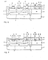
- the structure shown in FIG. 4 is obtained. As shown in FIG.
- a second photoresist layer 33 is now applied and provided with a pattern in which the emitter window 17 and the base contact window 19 are covered and the silicon dioxide layer is exposed in the region of the collector contact window 21 and the Schottky contacts 23 and 25.
- a further etching process now follows, in which the remainder of the silicon dioxide layer 11 still present in the region of the windows 21, 23 and 25 is removed (FIG. 5). This etching process can in turn be carried out in buffered hydrofluoric acid.
- the second photoresist layer 33 is also removed and the structure is cleaned.
- a thin (20 to 100 nm), preferably about 25 nm thick protective layer 35 made of silicon dioxide (FIG. 6) is applied in the region of the windows mentioned. This protective layer 35 is preferably grown thermally.
- a third photoresist mask 37 is applied, which only covers the emitter window 17, the collector contact window 21 and the cathode contact window 23 of the Schottky diode (FIG. 6).
- the N + -doped zones that is, the emitter zone 39, the collector contact zone and the cathode contact zone of the Schottky diode are formed by implantation of, for example, arsenic or phosphorus.
- a high-energy implantation process at an implantation of arsenic at 50 kV (range 40 to 60 kV) at a nominal dosage of 9.5 x 1 0 15 A t o me / cm 2 (with a current of about 2 mA range 1 , 8 to 2.2 mA).
- the process parameters are set so that the desired characteristics are generated.
- the dosage is in the range of about 8.5 x 1 0 15 to 1 0 x 10 15 atoms / cm 2.
- the ion implantation takes about 2 to 3 minutes.
- the third photoresist layer 37 is then removed.
- the protective layer 35 made of silicon dioxide not only prevents damage to the semiconductor surface during ion implantation, but also captures a considerable part of implanted impurities. It is therefore important to set the thickness of the protective layer exactly (in a range of + 10%) to ensure a parametric distribution. In its uppermost layer areas, the protective layer also absorbs metallic impurities in a thickness of approximately 10 to 15 nm, which are supplied by the implantation device. In order to prevent corresponding damage or impurities from migrating into the semiconductor material during the subsequent heating step serving to drive in the emitter zone, the uppermost layer region of the protective layer 35 is removed in a thickness of 10 to 15 nm by immersion etching in buffered hydrofluoric acid.
- the emitter zone 39 is driven into the base zone 12 by gradually heating the structure in a time-temperature sequence of 805 ° C. for 10 minutes, 1000 ° C. for 69 to 72 minutes and 825 ° C. for 10 minutes.
- the remaining part of the protective layer 35 prevents the diffusion out of the Impurities from the semiconductor material.
- the protective layer 35 is now completely removed by immersion etching. In subsequent process steps, which are no longer shown, the contacts and the conductive interconnections are produced in a conventional manner.
- the method according to the invention provides the transistors with improved characteristics and increased yields, which are normally limited by emitter-collector leakage currents. At the same time, the advantages given by the ion implantation of the emitter over diffusion are exploited.
Landscapes
- Bipolar Transistors (AREA)
- Electrodes Of Semiconductors (AREA)
- Element Separation (AREA)
- Bipolar Integrated Circuits (AREA)
Applications Claiming Priority (2)
| Application Number | Priority Date | Filing Date | Title |
|---|---|---|---|
| US06/051,078 US4243435A (en) | 1979-06-22 | 1979-06-22 | Bipolar transistor fabrication process with an ion implanted emitter |
| US51078 | 1987-05-15 |
Publications (2)
| Publication Number | Publication Date |
|---|---|
| EP0020998A1 true EP0020998A1 (fr) | 1981-01-07 |
| EP0020998B1 EP0020998B1 (fr) | 1983-04-13 |
Family
ID=21969190
Family Applications (1)
| Application Number | Title | Priority Date | Filing Date |
|---|---|---|---|
| EP80102657A Expired EP0020998B1 (fr) | 1979-06-22 | 1980-05-13 | Procédé de fabrication d'un transistor bipolaire comprenant une zône d'émetteur à implantation ionique |
Country Status (6)
| Country | Link |
|---|---|
| US (1) | US4243435A (fr) |
| EP (1) | EP0020998B1 (fr) |
| JP (1) | JPS564268A (fr) |
| CA (1) | CA1139015A (fr) |
| DE (1) | DE3062705D1 (fr) |
| IT (1) | IT1149957B (fr) |
Cited By (1)
| Publication number | Priority date | Publication date | Assignee | Title |
|---|---|---|---|---|
| EP0107437A1 (fr) * | 1982-10-22 | 1984-05-02 | Fujitsu Limited | Procédé de fabrication d'un dispositif semi-conducteur comprenant un transistor bipolaire et une diode à barrière de Schottky |
Families Citing this family (22)
| Publication number | Priority date | Publication date | Assignee | Title |
|---|---|---|---|---|
| US4452645A (en) * | 1979-11-13 | 1984-06-05 | International Business Machines Corporation | Method of making emitter regions by implantation through a non-monocrystalline layer |
| JPS5758356A (en) * | 1980-09-26 | 1982-04-08 | Toshiba Corp | Manufacture of semiconductor device |
| JPS57162460A (en) * | 1981-03-31 | 1982-10-06 | Fujitsu Ltd | Manufacture of semiconductor device |
| US4372033A (en) * | 1981-09-08 | 1983-02-08 | Ncr Corporation | Method of making coplanar MOS IC structures |
| JPS59124141A (ja) * | 1982-12-28 | 1984-07-18 | Toshiba Corp | 半導体装置の製造方法 |
| JPH0638422B2 (ja) * | 1985-04-11 | 1994-05-18 | ロ−ム株式会社 | 半導体装置の製造方法 |
| JP2501317B2 (ja) * | 1985-04-11 | 1996-05-29 | ローム 株式会社 | 半導体装置の製造方法 |
| JPH0719838B2 (ja) * | 1985-07-19 | 1995-03-06 | 松下電器産業株式会社 | 半導体装置およびその製造方法 |
| US4829025A (en) * | 1987-10-02 | 1989-05-09 | Advanced Micro Devices, Inc. | Process for patterning films in manufacture of integrated circuit structures |
| JPH0621368Y2 (ja) * | 1988-12-13 | 1994-06-08 | 九州日立マクセル株式会社 | 整髪美容器 |
| US5118634A (en) * | 1990-09-26 | 1992-06-02 | Purdue Research Foundation | Self-aligned integrated circuit bipolar transistor having monocrystalline contacts |
| US5364801A (en) * | 1990-12-17 | 1994-11-15 | Texas Instruments Incorporated | Method of forming a charge pump circuit |
| JPH0720974U (ja) * | 1991-04-23 | 1995-04-18 | 株式会社徳安 | 耳掻き |
| US5880036A (en) * | 1992-06-15 | 1999-03-09 | Micron Technology, Inc. | Method for enhancing oxide to nitride selectivity through the use of independent heat control |
| US5651855A (en) * | 1992-07-28 | 1997-07-29 | Micron Technology, Inc. | Method of making self aligned contacts to silicon substrates during the manufacture of integrated circuits |
| JP2666233B2 (ja) * | 1992-12-25 | 1997-10-22 | 鐘紡株式会社 | スポンジ状こんにゃく成形体 |
| US6835634B1 (en) | 1995-08-25 | 2004-12-28 | Micron Technology, Inc. | Streamlined field isolation process |
| US5920782A (en) * | 1997-07-18 | 1999-07-06 | United Microelectronics Corp. | Method for improving hot carrier degradation |
| US6337260B1 (en) | 1999-09-24 | 2002-01-08 | Advanced Micro Devices, Inc. | Use of knocked-on oxygen atoms for reduction of transient enhanced diffusion |
| JP5171232B2 (ja) * | 2006-12-15 | 2013-03-27 | 株式会社半導体エネルギー研究所 | 半導体装置の作製方法 |
| US7691734B2 (en) * | 2007-03-01 | 2010-04-06 | International Business Machines Corporation | Deep trench based far subcollector reachthrough |
| CN206098394U (zh) * | 2016-10-14 | 2017-04-12 | 京东方科技集团股份有限公司 | 一种显示基板、显示面板及显示装置 |
Citations (7)
| Publication number | Priority date | Publication date | Assignee | Title |
|---|---|---|---|---|
| FR1544067A (fr) * | 1966-12-01 | 1968-10-31 | Rca Corp | Dispositifs semi-conducteurs perfectionnés et procédé pour leur fabrication |
| US3468728A (en) * | 1964-12-31 | 1969-09-23 | Texas Instruments Inc | Method for forming ohmic contact for a semiconductor device |
| US3474021A (en) * | 1966-01-12 | 1969-10-21 | Ibm | Method of forming openings using sequential sputtering and chemical etching |
| US3933528A (en) * | 1974-07-02 | 1976-01-20 | Texas Instruments Incorporated | Process for fabricating integrated circuits utilizing ion implantation |
| FR2279223A1 (fr) * | 1974-07-15 | 1976-02-13 | Ibm | Procede d'implantation d'ions dans un substrat semi-conducteur au travers d'un revetement protecteur |
| US4110125A (en) * | 1977-03-03 | 1978-08-29 | International Business Machines Corporation | Method for fabricating semiconductor devices |
| US4118250A (en) * | 1977-12-30 | 1978-10-03 | International Business Machines Corporation | Process for producing integrated circuit devices by ion implantation |
Family Cites Families (11)
| Publication number | Priority date | Publication date | Assignee | Title |
|---|---|---|---|---|
| US3604986A (en) * | 1970-03-17 | 1971-09-14 | Bell Telephone Labor Inc | High frequency transistors with shallow emitters |
| DE2157633C3 (de) * | 1971-11-20 | 1980-01-24 | Deutsche Itt Industries Gmbh, 7800 Freiburg | Verfahren zum Herstellen von Zonen einer monolithisch integrierten Festkörperschaltung |
| CA998778A (en) * | 1972-07-13 | 1976-10-19 | Martin M. Skowron | Semiconductor manufacturing process |
| US3928081A (en) * | 1973-10-26 | 1975-12-23 | Signetics Corp | Method for fabricating semiconductor devices using composite mask and ion implantation |
| US3928082A (en) * | 1973-12-28 | 1975-12-23 | Texas Instruments Inc | Self-aligned transistor process |
| JPS51144184A (en) * | 1975-06-05 | 1976-12-10 | Mitsubishi Electric Corp | Production method of semiconductor unit |
| US4018627A (en) * | 1975-09-22 | 1977-04-19 | Signetics Corporation | Method for fabricating semiconductor devices utilizing oxide protective layer |
| FR2341943A1 (fr) * | 1976-02-20 | 1977-09-16 | Radiotechnique Compelec | Procede de realisation de transistors par implantation ionique |
| US4046606A (en) * | 1976-05-10 | 1977-09-06 | Rca Corporation | Simultaneous location of areas having different conductivities |
| US4135954A (en) * | 1977-07-12 | 1979-01-23 | International Business Machines Corporation | Method for fabricating self-aligned semiconductor devices utilizing selectively etchable masking layers |
| US4131497A (en) * | 1977-07-12 | 1978-12-26 | International Business Machines Corporation | Method of manufacturing self-aligned semiconductor devices |
-
1979
- 1979-06-22 US US06/051,078 patent/US4243435A/en not_active Expired - Lifetime
-
1980
- 1980-03-18 JP JP3349580A patent/JPS564268A/ja active Pending
- 1980-04-14 CA CA000349764A patent/CA1139015A/fr not_active Expired
- 1980-05-13 DE DE8080102657T patent/DE3062705D1/de not_active Expired
- 1980-05-13 EP EP80102657A patent/EP0020998B1/fr not_active Expired
- 1980-05-13 IT IT21995/80A patent/IT1149957B/it active
Patent Citations (8)
| Publication number | Priority date | Publication date | Assignee | Title |
|---|---|---|---|---|
| US3468728A (en) * | 1964-12-31 | 1969-09-23 | Texas Instruments Inc | Method for forming ohmic contact for a semiconductor device |
| US3474021A (en) * | 1966-01-12 | 1969-10-21 | Ibm | Method of forming openings using sequential sputtering and chemical etching |
| FR1544067A (fr) * | 1966-12-01 | 1968-10-31 | Rca Corp | Dispositifs semi-conducteurs perfectionnés et procédé pour leur fabrication |
| US3933528A (en) * | 1974-07-02 | 1976-01-20 | Texas Instruments Incorporated | Process for fabricating integrated circuits utilizing ion implantation |
| FR2279223A1 (fr) * | 1974-07-15 | 1976-02-13 | Ibm | Procede d'implantation d'ions dans un substrat semi-conducteur au travers d'un revetement protecteur |
| US3945856A (en) * | 1974-07-15 | 1976-03-23 | Ibm Corporation | Method of ion implantation through an electrically insulative material |
| US4110125A (en) * | 1977-03-03 | 1978-08-29 | International Business Machines Corporation | Method for fabricating semiconductor devices |
| US4118250A (en) * | 1977-12-30 | 1978-10-03 | International Business Machines Corporation | Process for producing integrated circuit devices by ion implantation |
Non-Patent Citations (3)
| Title |
|---|
| IBM TECHNICAL DISCLOSURE BULLETIN, Vol. 14, April 1972, Nr. 11, New York, USA C.W. SCHEFFER und L.L. WU: "SCHOTTKY barrier diode clamp fabrication", Seite 3410. * Seite 3410 * * |
| IBM TECHNICAL DISCLOSURE BULLETIN, Vol. 20, April 1978, Nr. 11A, New York, USA C.A. BARILE et al. "Ion implanting an emitter", Seiten 4351-4352. * Seiten 4351-4352 * * |
| INSTITUTE OF ELECTRICAL AND ELECTRONICS ENGINEERS INTERNATIONAL ELECTRON DEVICES MEETING, technical digest, Dezember 6-8, 1976, New York, USA A. AITKEN et al. "A fully plasma etched-ion implanted CMOS process", Seiten 209-213. * Seite 209, Spalte 2, Absatz 2 - Seite 210, Spalte 1, Absatz 2 * * |
Cited By (1)
| Publication number | Priority date | Publication date | Assignee | Title |
|---|---|---|---|---|
| EP0107437A1 (fr) * | 1982-10-22 | 1984-05-02 | Fujitsu Limited | Procédé de fabrication d'un dispositif semi-conducteur comprenant un transistor bipolaire et une diode à barrière de Schottky |
Also Published As
| Publication number | Publication date |
|---|---|
| IT1149957B (it) | 1986-12-10 |
| DE3062705D1 (en) | 1983-05-19 |
| CA1139015A (fr) | 1983-01-04 |
| US4243435A (en) | 1981-01-06 |
| EP0020998B1 (fr) | 1983-04-13 |
| IT8021995A0 (it) | 1980-05-13 |
| JPS564268A (en) | 1981-01-17 |
Similar Documents
| Publication | Publication Date | Title |
|---|---|---|
| EP0020998B1 (fr) | Procédé de fabrication d'un transistor bipolaire comprenant une zône d'émetteur à implantation ionique | |
| DE2745857C2 (fr) | ||
| EP0001550B1 (fr) | Dispositif semiconducteur à intégration avec de petites structures et procédé pour sa fabrication | |
| DE69012611T2 (de) | Verfahren zum Herstellen bipolarer vertikaler Transistoren und von Hochspannungs-CMOS-Transistoren in einer einzigen integrierten Schaltung. | |
| DE10214066B4 (de) | Halbleiterbauelement mit retrogradem Dotierprofil in einem Kanalgebiet und Verfahren zur Herstellung desselben | |
| DE3881799T2 (de) | Verfahren zur Herstellung von CMOS-Bauelementen. | |
| EP0032550B1 (fr) | Procédé de fabrication d'une structure verticale de transistor PNP bipolaire | |
| DE3019850C2 (fr) | ||
| EP0000327B1 (fr) | Procédé de fabrication de dispositifs semiconducteurs intégrés auto-alignés | |
| EP0001574B1 (fr) | Dispositif semiconducteur pour structures de résistance dans des circuits intégrés de haute densité et procédé pour sa fabrication | |
| DE3205022A1 (de) | Verfahren zum herstellen einer integrierten halbleiterschaltung | |
| EP0071665B1 (fr) | Procédé pour la fabrication d'un circuit intégré à corps solide et monolithique ayant au moins un transistor bipolaire plan | |
| EP0005185B1 (fr) | Procédé pour la formation simultanée de diodes à barrage Schottky et de contacts ohmiques sur des régions semi-conductrices dopées | |
| DE3511229A1 (de) | Verfahren zur herstellung isolierter bipolartransistoren in verbindung mit cmos-halbleiterstrukturen | |
| EP0007923A1 (fr) | Procédé pour la fabrication d'un transistor latéral à double diffusion et d'un transistor complémentaire vertical, intégré avec le premier | |
| EP0006510B1 (fr) | Procédé de formation de régions adjacentes et dopées différemment dans un substrat de silicium | |
| DE19909993A1 (de) | Verfahren zum Bilden von Bipolartransistoren mit selbstausrichtender epitaktischer Basis | |
| EP0025854A1 (fr) | Procédé de fabrication de transistors bipolaires | |
| DE2729973C2 (de) | Verfahren zur Herstellung einer Halbleiteranordnung | |
| DE2420239A1 (de) | Verfahren zur herstellung doppelt diffundierter lateraler transistoren | |
| DE2749607B2 (de) | Halbleiteranordnung und Verfahren zu deren Herstellung | |
| DE3540422C2 (de) | Verfahren zum Herstellen integrierter Strukturen mit nicht-flüchtigen Speicherzellen, die selbst-ausgerichtete Siliciumschichten und dazugehörige Transistoren aufweisen | |
| DE69216304T2 (de) | Verfahren zum Herstellen eines selbst-ausrichtenden, planaren, monolithischen integrierten Schaltkreises mit vertikalen Transistoren | |
| DE10351008A1 (de) | Verbesserte Technik zur Herstellung von Transistoren mit erhöhten Drain- und Sourcegebieten mit unterschiedlicher Höhe | |
| DE2640981C2 (de) | Verfahren zur Herstellung von Halbleiteranordnungen durch Ionenimplantation |
Legal Events
| Date | Code | Title | Description |
|---|---|---|---|
| PUAI | Public reference made under article 153(3) epc to a published international application that has entered the european phase |
Free format text: ORIGINAL CODE: 0009012 |
|
| AK | Designated contracting states |
Designated state(s): DE FR GB |
|
| 17P | Request for examination filed |
Effective date: 19810605 |
|
| GRAA | (expected) grant |
Free format text: ORIGINAL CODE: 0009210 |
|
| AK | Designated contracting states |
Designated state(s): DE FR GB |
|
| REF | Corresponds to: |
Ref document number: 3062705 Country of ref document: DE Date of ref document: 19830519 |
|
| ET | Fr: translation filed | ||
| PGFP | Annual fee paid to national office [announced via postgrant information from national office to epo] |
Ref country code: GB Payment date: 19900404 Year of fee payment: 11 |
|
| PGFP | Annual fee paid to national office [announced via postgrant information from national office to epo] |
Ref country code: FR Payment date: 19910430 Year of fee payment: 12 |
|
| PG25 | Lapsed in a contracting state [announced via postgrant information from national office to epo] |
Ref country code: GB Effective date: 19910513 |
|
| PGFP | Annual fee paid to national office [announced via postgrant information from national office to epo] |
Ref country code: DE Payment date: 19910525 Year of fee payment: 12 |
|
| GBPC | Gb: european patent ceased through non-payment of renewal fee | ||
| PG25 | Lapsed in a contracting state [announced via postgrant information from national office to epo] |
Ref country code: FR Effective date: 19930129 |
|
| PG25 | Lapsed in a contracting state [announced via postgrant information from national office to epo] |
Ref country code: DE Effective date: 19930202 |
|
| REG | Reference to a national code |
Ref country code: FR Ref legal event code: ST |
|
| PLBE | No opposition filed within time limit |
Free format text: ORIGINAL CODE: 0009261 |
|
| STAA | Information on the status of an ep patent application or granted ep patent |
Free format text: STATUS: NO OPPOSITION FILED WITHIN TIME LIMIT |