EP0021085A2 - Amplificateur à transistor monolithiquement intégrable - Google Patents
Amplificateur à transistor monolithiquement intégrable Download PDFInfo
- Publication number
- EP0021085A2 EP0021085A2 EP80102972A EP80102972A EP0021085A2 EP 0021085 A2 EP0021085 A2 EP 0021085A2 EP 80102972 A EP80102972 A EP 80102972A EP 80102972 A EP80102972 A EP 80102972A EP 0021085 A2 EP0021085 A2 EP 0021085A2
- Authority
- EP
- European Patent Office
- Prior art keywords
- transistor
- base
- transistors
- emitter
- collector
- Prior art date
- Legal status (The legal status is an assumption and is not a legal conclusion. Google has not performed a legal analysis and makes no representation as to the accuracy of the status listed.)
- Granted
Links
- 239000004065 semiconductor Substances 0.000 description 3
- 239000000758 substrate Substances 0.000 description 3
- 238000005516 engineering process Methods 0.000 description 2
- 230000003071 parasitic effect Effects 0.000 description 2
- 238000013459 approach Methods 0.000 description 1
- 230000000295 complement effect Effects 0.000 description 1
- 230000008878 coupling Effects 0.000 description 1
- 238000010168 coupling process Methods 0.000 description 1
- 238000005859 coupling reaction Methods 0.000 description 1
- 238000000034 method Methods 0.000 description 1
Images
Classifications
-
- H—ELECTRICITY
- H03—ELECTRONIC CIRCUITRY
- H03F—AMPLIFIERS
- H03F3/00—Amplifiers with only discharge tubes or only semiconductor devices as amplifying elements
- H03F3/45—Differential amplifiers
- H03F3/45071—Differential amplifiers with semiconductor devices only
- H03F3/45076—Differential amplifiers with semiconductor devices only characterised by the way of implementation of the active amplifying circuit in the differential amplifier
- H03F3/45179—Differential amplifiers with semiconductor devices only characterised by the way of implementation of the active amplifying circuit in the differential amplifier using MOSFET transistors as the active amplifying circuit
- H03F3/45197—Pl types
-
- H—ELECTRICITY
- H03—ELECTRONIC CIRCUITRY
- H03F—AMPLIFIERS
- H03F3/00—Amplifiers with only discharge tubes or only semiconductor devices as amplifying elements
- H03F3/45—Differential amplifiers
-
- H—ELECTRICITY
- H03—ELECTRONIC CIRCUITRY
- H03F—AMPLIFIERS
- H03F3/00—Amplifiers with only discharge tubes or only semiconductor devices as amplifying elements
- H03F3/45—Differential amplifiers
- H03F3/45071—Differential amplifiers with semiconductor devices only
- H03F3/45076—Differential amplifiers with semiconductor devices only characterised by the way of implementation of the active amplifying circuit in the differential amplifier
- H03F3/4508—Differential amplifiers with semiconductor devices only characterised by the way of implementation of the active amplifying circuit in the differential amplifier using bipolar transistors as the active amplifying circuit
- H03F3/45098—PI types
-
- H—ELECTRICITY
- H03—ELECTRONIC CIRCUITRY
- H03G—CONTROL OF AMPLIFICATION
- H03G1/00—Details of arrangements for controlling amplification
- H03G1/0005—Circuits characterised by the type of controlling devices operated by a controlling current or voltage signal
- H03G1/0017—Circuits characterised by the type of controlling devices operated by a controlling current or voltage signal the device being at least one of the amplifying solid-state elements
- H03G1/0023—Circuits characterised by the type of controlling devices operated by a controlling current or voltage signal the device being at least one of the amplifying solid-state elements in emitter-coupled or cascode amplifiers
-
- H—ELECTRICITY
- H03—ELECTRONIC CIRCUITRY
- H03G—CONTROL OF AMPLIFICATION
- H03G3/00—Gain control in amplifiers or frequency changers
- H03G3/02—Manually-operated control
- H03G3/04—Manually-operated control in untuned amplifiers
- H03G3/10—Manually-operated control in untuned amplifiers having semiconductor devices
Definitions
- the invention relates to a monolithically integrable transistor amplifier, the signal input to the base of a first transistor and in which the emitter of this first transistor is connected to the emitter of a second transistor of the same type, in which a voltage source, in particular a constant current source, with its a connection to the emitters of the two transistors and to the other connection via a load resistor to the collectors of the two transistors and in which the signal output is finally connected to the collector of the second transistor.
- a voltage source in particular a constant current source
- Transistor amplifier circuits of this type are known and are referred to and used as differential amplifiers.
- differential amplifiers For example, the book by U. Tietze-Ch. Schenk called “semiconductor circuit technology” (1978), page 59.
- the known amplifiers had to be provided with complex control circuits, which, in addition in the case of monolithic display, led to considerable parasitic substrate currents and also to such a high control current requirement, which was no longer related to the modulation capability achieved. The following can be stated in detail:
- the signal processing in integrated amplifiers is preferably carried out in a symmetrical form.
- the linear range of a differential level is approx. 2.
- U T where Um is the temperature voltage. It can be increased by emitter resistors by the amount of voltage drop across these resistors.
- transistors connected as diodes in the emitter branch of differential stages. In this way, compared to the normal emitter-coupled differential stages without negative feedback, a noticeably increased modulation capability is also achieved.
- such a procedure in a monolithically integrated semiconductor circuit leads to the fact that the operation of the structures just specified activates the complementary substrate transistor in the residual voltage range, which leads to a disproportionate control current requirement or recorded control current leads to scattering of the gain. Since the useful control current reaches the active part of the control circuit, there is also a change in the operating point of the differential stage and an undesirable change in the collector operating voltage.
- the invention is intended to remedy this:
- the initially defined monolithically integrable transistor amplifier is designed such that four transistors of the same type are provided and two of these four transistors form the first transistor and the second transistor, that in addition the base of the second transistor is connected to the base of the third transistor and the third transistor is connected to the fourth transistor in the same way as the first transistor is connected to the second transistor, that further the collector of the first transistor is directly connected to the collector of the third transistor on the one hand and the collector of the second transistor is connected to the collector of the fourth transistor on the other hand that continue to have a common between both the base connections of the four transistors same connection and between the emitter connections of the four transistors there is also a common connection and that a signal or potential to be supplied via a reference input is finally provided for the application of the base connections of the second and third transistors.
- control stage can always be operated with the same collector-emitter voltage.
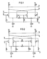
- the essentially new thing is that the collectors are combined in pairs in accordance with the phase of the collector signal and are located at two outputs, as shown by a further development of the invention shown in FIGS. 1 and 2.
- the gain control can be carried out either by current distribution control (Fig. 1) or by negative feedback control (Fig. 2).
- FIGS. 1 and 2 The invention will now be described in more detail with reference to FIGS. 1 and 2:
- a DC voltage potential V EE or the one pole of a constant current source 11 or 12 is connected to the emitters of the transistor pairs 1, 2 and 3, 4 either via a series resistor.
- the other connection of the DC voltage potential V EE lie
- the remote voltage source or the other pole of the constant current source 11 or 12 is connected to the collectors of the transistors 1, 3 or 2, 4 via a load resistor 9 or 10, respectively. These are dimensioned according to the desired step gain.
- the four transistors 1, 2, 3 and 4 are of the same type, ie either npn transistors or pnp transistors.
- the emitter of transistor 1 and the emitter of transistor 2 are connected to one another and are either connected via a series resistor with the operating potential V GG corresponding to their conductivity type or, as in FIGS. 1 and 2, with one pole of a constant current source 11.
- the base of transistor 1 forms one signal input 13.
- the collector of transistor 1 is connected to signal output 15 and also via load resistor 9 to second operating potential V CC or to the other pole of constant current source 11.
- the transistor 3 has its emitter connected to the emitter of the transistor 4. Both emitters are either connected to the same potential V EE via a series resistor at which the emitters of transistors 1 and 2 are already connected. Or there is a second constant current source 12 to which the emitters of transistors 3 and 4 are connected.
- the collector of the transistor 4 is connected to the second operating potential V CC via a load resistor 10, in the second case via the load resistor 10 to the second connection of the constant current source 12. Details of the structure of constant current sources can be found, for example, in the book by Tietze-Schenk mentioned " Semiconductor circuit technology "(1978), pages 53 to 59. , The collector of transistor 4 forms the other output terminal 16 of the transistor amplifier.
- the collector of transistor 2 is with the collector of transistor 4, the collector . of transistor 1 connected to the collector of transistor 3. 1, the base of transistor 2 is located directly on the base of transistor 3. Furthermore, the emitters of transistors 1 and 2 are connected via a negative feedback resistor 8 to the emitters of transistors 3 and 4, which means that in the definition the invention mentioned common connection between the emitters of the four transistors 1 to 4 is given. Furthermore, a reference input 17 to be acted upon by a reference potential or reference signal is provided, which is connected via a resistor 5 or 6 or 7 to the base of transistor 1, or transistors 2 and 3, or transistor 4. Finally, the base of transistor 4 is at the second input terminal 14 of the amplifier.
- the so-called current distribution control is not selected, as in FIG. 1, but the so-called negative feedback control.
- the connection between the base connections of the two transistors 2 and 3 is separated by a circuit-switching circuit R v , which is given, for example, by a conventional control circuit, such as a control circuit with two diodes or a diode ring, and then the connection between the base connections of the second transistor and the third transistor, that is, transistors 2 and 3.
- the minimum gain is obtained when the internal resistance of the circuit element Ry is infinite goes and when the size of the negative feedback resistor 8 determines the gain.
- the maximum gain is given when the internal resistance of the circuit element R V approaches zero.
Landscapes
- Engineering & Computer Science (AREA)
- Power Engineering (AREA)
- Amplifiers (AREA)
- Control Of Amplification And Gain Control (AREA)
Applications Claiming Priority (2)
| Application Number | Priority Date | Filing Date | Title |
|---|---|---|---|
| DE2924171 | 1979-06-15 | ||
| DE19792924171 DE2924171A1 (de) | 1979-06-15 | 1979-06-15 | Monolithisch integrierbarer transistorverstaerker |
Publications (3)
| Publication Number | Publication Date |
|---|---|
| EP0021085A2 true EP0021085A2 (fr) | 1981-01-07 |
| EP0021085A3 EP0021085A3 (en) | 1981-03-18 |
| EP0021085B1 EP0021085B1 (fr) | 1984-04-11 |
Family
ID=6073269
Family Applications (1)
| Application Number | Title | Priority Date | Filing Date |
|---|---|---|---|
| EP80102972A Expired EP0021085B1 (fr) | 1979-06-15 | 1980-05-28 | Amplificateur à transistor monolithiquement intégrable |
Country Status (4)
| Country | Link |
|---|---|
| US (1) | US4369410A (fr) |
| EP (1) | EP0021085B1 (fr) |
| JP (1) | JPS564908A (fr) |
| DE (1) | DE2924171A1 (fr) |
Cited By (1)
| Publication number | Priority date | Publication date | Assignee | Title |
|---|---|---|---|---|
| EP0397250A3 (fr) * | 1989-05-10 | 1991-10-02 | Philips Electronics Uk Limited | Amplificateur à blocage de courant continu |
Families Citing this family (8)
| Publication number | Priority date | Publication date | Assignee | Title |
|---|---|---|---|---|
| US4621831A (en) * | 1984-09-06 | 1986-11-11 | Nhk Spring Co., Ltd. | Stabilizer for motor vehicle |
| JPS6173156A (ja) * | 1984-09-19 | 1986-04-15 | Toray Ind Inc | 水なし平版印刷用原板 |
| JPH0682213B2 (ja) * | 1986-06-16 | 1994-10-19 | 東レ株式会社 | 水なし平版印刷用原版 |
| EP0600141B1 (fr) * | 1992-10-30 | 1997-03-05 | SGS-THOMSON MICROELECTRONICS S.p.A. | Etage transconductance |
| JPH07110574A (ja) * | 1993-12-13 | 1995-04-25 | Toray Ind Inc | 水なし平版印刷用原板の製造方法 |
| JPH08102629A (ja) * | 1994-09-30 | 1996-04-16 | Ando Electric Co Ltd | 差動増幅回路 |
| GB9906026D0 (en) | 1999-03-16 | 1999-05-12 | Mitel Semiconductor Ltd | An amplifier circuit arrangement |
| KR100485796B1 (ko) * | 2003-01-23 | 2005-04-28 | 삼성전자주식회사 | 부스팅 회로 |
Family Cites Families (11)
| Publication number | Priority date | Publication date | Assignee | Title |
|---|---|---|---|---|
| GB915404A (en) * | 1961-01-13 | 1963-01-09 | Marconi Wireless Telegraph Co | Improvements in or relating to variable gain circuit arrangements |
| US3452289A (en) * | 1967-02-16 | 1969-06-24 | Motorola Inc | Differential amplifier circuits |
| NL162802C (nl) * | 1971-10-09 | 1980-06-16 | Philips Nv | Geintegreerde verschilversterker. |
| DE2230431C3 (de) * | 1972-06-22 | 1982-12-16 | Robert Bosch Gmbh, 7000 Stuttgart | Schaltungsanordnung zur symmetrischen Ansteuerung eines Differenzverstärkers |
| US3843934A (en) * | 1973-01-31 | 1974-10-22 | Advanced Micro Devices Inc | High speed transistor difference amplifier |
| JPS49104549A (fr) * | 1973-02-07 | 1974-10-03 | ||
| US3846712A (en) * | 1973-03-12 | 1974-11-05 | Bell Telephone Labor Inc | Differential amplifier with dynamic biasing |
| JPS5921233B2 (ja) * | 1976-09-14 | 1984-05-18 | ソニー株式会社 | ステレオ復調回路 |
| US4109214A (en) * | 1977-05-31 | 1978-08-22 | Motorola, Inc. | Unbalanced-to-balanced signal converter circuit |
| JPS6045166B2 (ja) * | 1977-06-24 | 1985-10-08 | 株式会社クラレ | 3−(β−ヒドロキシエチル)ブテノ−ル類の製造方法 |
| US4146844A (en) * | 1977-10-31 | 1979-03-27 | Tektronix, Inc. | Feed-forward amplifier |
-
1979
- 1979-06-15 DE DE19792924171 patent/DE2924171A1/de active Granted
-
1980
- 1980-05-28 EP EP80102972A patent/EP0021085B1/fr not_active Expired
- 1980-06-05 US US06/156,863 patent/US4369410A/en not_active Expired - Lifetime
- 1980-06-12 JP JP7960080A patent/JPS564908A/ja active Pending
Cited By (1)
| Publication number | Priority date | Publication date | Assignee | Title |
|---|---|---|---|---|
| EP0397250A3 (fr) * | 1989-05-10 | 1991-10-02 | Philips Electronics Uk Limited | Amplificateur à blocage de courant continu |
Also Published As
| Publication number | Publication date |
|---|---|
| DE2924171C2 (fr) | 1987-12-17 |
| US4369410A (en) | 1983-01-18 |
| JPS564908A (en) | 1981-01-19 |
| EP0021085A3 (en) | 1981-03-18 |
| DE2924171A1 (de) | 1980-12-18 |
| EP0021085B1 (fr) | 1984-04-11 |
Similar Documents
| Publication | Publication Date | Title |
|---|---|---|
| DE3103969C2 (de) | "Versorgungsspannungstreiber für einen Differentialverstärker" | |
| DE3114877C2 (de) | Stromspiegelschaltung | |
| DE2837853C3 (de) | Differenzverstärker | |
| DE3012965C2 (fr) | ||
| DE1901804B2 (de) | Stabilisierter differentialverstaerker | |
| DE4113498C1 (fr) | ||
| DE3937501A1 (de) | Verfahren und vorrichtung zur erzeugung einer vorspannung | |
| DE69528845T2 (de) | N-bit umsetzer mit n-1-grössenverstärkern und n-vergleichern | |
| DE69725277T2 (de) | Rauscharmer Verstärker | |
| DE2416534A1 (de) | Komplementaer-symmetrische verstoerkerschaltung | |
| DE2648577A1 (de) | Elektrisch veraenderbare impedanzschaltung | |
| EP0021085B1 (fr) | Amplificateur à transistor monolithiquement intégrable | |
| DE2443137C2 (de) | Differentialverstärker | |
| DE2905659A1 (de) | Gegentakt-verstaerkerkreis | |
| DE69611967T2 (de) | Gefaltetes aktives Filter | |
| DE2409929C3 (de) | Verzerrungsarmer, niederfrequenter Gegentakt-Leistungsverstärker | |
| DE69018870T2 (de) | Bipolare Transistorschaltung mit Verzerrungsausgleich. | |
| DE3210661A1 (de) | Verstaerker | |
| EP0237086B1 (fr) | Circuit de miroir de courant | |
| DE3810058A1 (de) | Schmitt-trigger-schaltung | |
| DE69320776T2 (de) | Transkonduktanzverstärker | |
| DE2946952C2 (fr) | ||
| DE60133068T2 (de) | Differentiell angeordnetes transistorpaar mit mitteln zur degeneration der transkonduktanz | |
| DE3229437C2 (fr) | ||
| DE3243706C1 (de) | ECL-TTL-Signalpegelwandler |
Legal Events
| Date | Code | Title | Description |
|---|---|---|---|
| PUAI | Public reference made under article 153(3) epc to a published international application that has entered the european phase |
Free format text: ORIGINAL CODE: 0009012 |
|
| AK | Designated contracting states |
Designated state(s): FR GB IT |
|
| PUAL | Search report despatched |
Free format text: ORIGINAL CODE: 0009013 |
|
| AK | Designated contracting states |
Designated state(s): FR GB IT |
|
| 17P | Request for examination filed |
Effective date: 19810626 |
|
| ITF | It: translation for a ep patent filed | ||
| GRAA | (expected) grant |
Free format text: ORIGINAL CODE: 0009210 |
|
| AK | Designated contracting states |
Designated state(s): FR GB IT |
|
| ET | Fr: translation filed | ||
| PLBE | No opposition filed within time limit |
Free format text: ORIGINAL CODE: 0009261 |
|
| STAA | Information on the status of an ep patent application or granted ep patent |
Free format text: STATUS: NO OPPOSITION FILED WITHIN TIME LIMIT |
|
| 26N | No opposition filed | ||
| PGFP | Annual fee paid to national office [announced via postgrant information from national office to epo] |
Ref country code: GB Payment date: 19890430 Year of fee payment: 10 |
|
| PGFP | Annual fee paid to national office [announced via postgrant information from national office to epo] |
Ref country code: FR Payment date: 19890522 Year of fee payment: 10 |
|
| ITTA | It: last paid annual fee | ||
| PG25 | Lapsed in a contracting state [announced via postgrant information from national office to epo] |
Ref country code: GB Effective date: 19900528 |
|
| GBPC | Gb: european patent ceased through non-payment of renewal fee | ||
| PG25 | Lapsed in a contracting state [announced via postgrant information from national office to epo] |
Ref country code: FR Effective date: 19910131 |
|
| REG | Reference to a national code |
Ref country code: FR Ref legal event code: ST |