EP0021385B1 - Procédé de fabrication de barres en silicium - Google Patents
Procédé de fabrication de barres en silicium Download PDFInfo
- Publication number
- EP0021385B1 EP0021385B1 EP80103506A EP80103506A EP0021385B1 EP 0021385 B1 EP0021385 B1 EP 0021385B1 EP 80103506 A EP80103506 A EP 80103506A EP 80103506 A EP80103506 A EP 80103506A EP 0021385 B1 EP0021385 B1 EP 0021385B1
- Authority
- EP
- European Patent Office
- Prior art keywords
- silicon
- rod
- melt
- crystallization chamber
- protective
- Prior art date
- Legal status (The legal status is an assumption and is not a legal conclusion. Google has not performed a legal analysis and makes no representation as to the accuracy of the status listed.)
- Expired
Links
- XUIMIQQOPSSXEZ-UHFFFAOYSA-N Silicon Chemical compound [Si] XUIMIQQOPSSXEZ-UHFFFAOYSA-N 0.000 title claims description 112
- 229910052710 silicon Inorganic materials 0.000 title claims description 112
- 239000010703 silicon Substances 0.000 title claims description 112
- 238000000034 method Methods 0.000 title claims description 31
- 230000008569 process Effects 0.000 title claims description 19
- 238000002425 crystallisation Methods 0.000 claims description 61
- OKTJSMMVPCPJKN-UHFFFAOYSA-N Carbon Chemical compound [C] OKTJSMMVPCPJKN-UHFFFAOYSA-N 0.000 claims description 27
- 230000001681 protective effect Effects 0.000 claims description 25
- 239000010439 graphite Substances 0.000 claims description 24
- 229910002804 graphite Inorganic materials 0.000 claims description 24
- 239000013078 crystal Substances 0.000 claims description 20
- 239000000155 melt Substances 0.000 claims description 18
- 230000008018 melting Effects 0.000 claims description 16
- 238000002844 melting Methods 0.000 claims description 16
- 238000004519 manufacturing process Methods 0.000 claims description 14
- 238000001816 cooling Methods 0.000 claims description 8
- WUKWITHWXAAZEY-UHFFFAOYSA-L calcium difluoride Chemical compound [F-].[F-].[Ca+2] WUKWITHWXAAZEY-UHFFFAOYSA-L 0.000 claims description 7
- 229910001634 calcium fluoride Inorganic materials 0.000 claims description 7
- 229910052918 calcium silicate Inorganic materials 0.000 claims description 7
- 239000000378 calcium silicate Substances 0.000 claims description 7
- OYACROKNLOSFPA-UHFFFAOYSA-N calcium;dioxido(oxo)silane Chemical compound [Ca+2].[O-][Si]([O-])=O OYACROKNLOSFPA-UHFFFAOYSA-N 0.000 claims description 7
- 229910052915 alkaline earth metal silicate Inorganic materials 0.000 claims description 2
- 229910001618 alkaline earth metal fluoride Inorganic materials 0.000 claims 1
- 230000008025 crystallization Effects 0.000 description 57
- 239000010453 quartz Substances 0.000 description 19
- VYPSYNLAJGMNEJ-UHFFFAOYSA-N silicon dioxide Inorganic materials O=[Si]=O VYPSYNLAJGMNEJ-UHFFFAOYSA-N 0.000 description 19
- 238000010438 heat treatment Methods 0.000 description 15
- 239000000463 material Substances 0.000 description 11
- 239000007788 liquid Substances 0.000 description 9
- 239000000203 mixture Substances 0.000 description 7
- 238000007711 solidification Methods 0.000 description 6
- 230000008023 solidification Effects 0.000 description 6
- 238000004140 cleaning Methods 0.000 description 5
- 239000008187 granular material Substances 0.000 description 5
- IJGRMHOSHXDMSA-UHFFFAOYSA-N Atomic nitrogen Chemical compound N#N IJGRMHOSHXDMSA-UHFFFAOYSA-N 0.000 description 4
- ZOXJGFHDIHLPTG-UHFFFAOYSA-N Boron Chemical compound [B] ZOXJGFHDIHLPTG-UHFFFAOYSA-N 0.000 description 4
- 229910004261 CaF 2 Inorganic materials 0.000 description 4
- OAICVXFJPJFONN-UHFFFAOYSA-N Phosphorus Chemical compound [P] OAICVXFJPJFONN-UHFFFAOYSA-N 0.000 description 4
- 229910052796 boron Inorganic materials 0.000 description 4
- 238000006073 displacement reaction Methods 0.000 description 4
- 229910052698 phosphorus Inorganic materials 0.000 description 4
- 239000011574 phosphorus Substances 0.000 description 4
- 239000007787 solid Substances 0.000 description 4
- 229910004762 CaSiO Inorganic materials 0.000 description 3
- 238000005266 casting Methods 0.000 description 3
- 239000002019 doping agent Substances 0.000 description 3
- 239000012535 impurity Substances 0.000 description 3
- 230000006698 induction Effects 0.000 description 3
- ORUIBWPALBXDOA-UHFFFAOYSA-L magnesium fluoride Chemical compound [F-].[F-].[Mg+2] ORUIBWPALBXDOA-UHFFFAOYSA-L 0.000 description 3
- 229910001635 magnesium fluoride Inorganic materials 0.000 description 3
- HBMJWWWQQXIZIP-UHFFFAOYSA-N silicon carbide Chemical compound [Si+]#[C-] HBMJWWWQQXIZIP-UHFFFAOYSA-N 0.000 description 3
- 229910010271 silicon carbide Inorganic materials 0.000 description 3
- XKRFYHLGVUSROY-UHFFFAOYSA-N Argon Chemical compound [Ar] XKRFYHLGVUSROY-UHFFFAOYSA-N 0.000 description 2
- OYPRJOBELJOOCE-UHFFFAOYSA-N Calcium Chemical compound [Ca] OYPRJOBELJOOCE-UHFFFAOYSA-N 0.000 description 2
- 229910052581 Si3N4 Inorganic materials 0.000 description 2
- 230000008901 benefit Effects 0.000 description 2
- 230000015572 biosynthetic process Effects 0.000 description 2
- 229910052791 calcium Inorganic materials 0.000 description 2
- 239000011575 calcium Substances 0.000 description 2
- 229910052799 carbon Inorganic materials 0.000 description 2
- 238000006243 chemical reaction Methods 0.000 description 2
- 239000011248 coating agent Substances 0.000 description 2
- 238000000576 coating method Methods 0.000 description 2
- 239000002826 coolant Substances 0.000 description 2
- 150000002222 fluorine compounds Chemical class 0.000 description 2
- 230000008014 freezing Effects 0.000 description 2
- 238000007710 freezing Methods 0.000 description 2
- 238000005470 impregnation Methods 0.000 description 2
- 238000009413 insulation Methods 0.000 description 2
- HCWCAKKEBCNQJP-UHFFFAOYSA-N magnesium orthosilicate Chemical compound [Mg+2].[Mg+2].[O-][Si]([O-])([O-])[O-] HCWCAKKEBCNQJP-UHFFFAOYSA-N 0.000 description 2
- 229910052919 magnesium silicate Inorganic materials 0.000 description 2
- 239000000391 magnesium silicate Substances 0.000 description 2
- 235000019792 magnesium silicate Nutrition 0.000 description 2
- 229910052757 nitrogen Inorganic materials 0.000 description 2
- 229910021420 polycrystalline silicon Inorganic materials 0.000 description 2
- 230000009467 reduction Effects 0.000 description 2
- 239000004065 semiconductor Substances 0.000 description 2
- HQVNEWCFYHHQES-UHFFFAOYSA-N silicon nitride Chemical compound N12[Si]34N5[Si]62N3[Si]51N64 HQVNEWCFYHHQES-UHFFFAOYSA-N 0.000 description 2
- KRHYYFGTRYWZRS-UHFFFAOYSA-M Fluoride anion Chemical compound [F-] KRHYYFGTRYWZRS-UHFFFAOYSA-M 0.000 description 1
- GYHNNYVSQQEPJS-UHFFFAOYSA-N Gallium Chemical compound [Ga] GYHNNYVSQQEPJS-UHFFFAOYSA-N 0.000 description 1
- FYYHWMGAXLPEAU-UHFFFAOYSA-N Magnesium Chemical compound [Mg] FYYHWMGAXLPEAU-UHFFFAOYSA-N 0.000 description 1
- NHWNVPNZGGXQQV-UHFFFAOYSA-J [Si+4].[O-]N=O.[O-]N=O.[O-]N=O.[O-]N=O Chemical compound [Si+4].[O-]N=O.[O-]N=O.[O-]N=O.[O-]N=O NHWNVPNZGGXQQV-UHFFFAOYSA-J 0.000 description 1
- 230000009471 action Effects 0.000 description 1
- 229910052782 aluminium Inorganic materials 0.000 description 1
- XAGFODPZIPBFFR-UHFFFAOYSA-N aluminium Chemical compound [Al] XAGFODPZIPBFFR-UHFFFAOYSA-N 0.000 description 1
- 229910052787 antimony Inorganic materials 0.000 description 1
- WATWJIUSRGPENY-UHFFFAOYSA-N antimony atom Chemical compound [Sb] WATWJIUSRGPENY-UHFFFAOYSA-N 0.000 description 1
- 229910052786 argon Inorganic materials 0.000 description 1
- 229910052785 arsenic Inorganic materials 0.000 description 1
- RQNWIZPPADIBDY-UHFFFAOYSA-N arsenic atom Chemical compound [As] RQNWIZPPADIBDY-UHFFFAOYSA-N 0.000 description 1
- 239000010425 asbestos Substances 0.000 description 1
- 229910052788 barium Inorganic materials 0.000 description 1
- DSAJWYNOEDNPEQ-UHFFFAOYSA-N barium atom Chemical compound [Ba] DSAJWYNOEDNPEQ-UHFFFAOYSA-N 0.000 description 1
- 238000007664 blowing Methods 0.000 description 1
- 229940043430 calcium compound Drugs 0.000 description 1
- 238000011088 calibration curve Methods 0.000 description 1
- 239000000969 carrier Substances 0.000 description 1
- 150000001875 compounds Chemical class 0.000 description 1
- 238000010924 continuous production Methods 0.000 description 1
- 239000000112 cooling gas Substances 0.000 description 1
- 230000003111 delayed effect Effects 0.000 description 1
- 238000009826 distribution Methods 0.000 description 1
- 238000005516 engineering process Methods 0.000 description 1
- 238000002474 experimental method Methods 0.000 description 1
- 239000010419 fine particle Substances 0.000 description 1
- 239000002803 fossil fuel Substances 0.000 description 1
- 229910052733 gallium Inorganic materials 0.000 description 1
- 229910021397 glassy carbon Inorganic materials 0.000 description 1
- 238000007654 immersion Methods 0.000 description 1
- 230000008676 import Effects 0.000 description 1
- 229910052738 indium Inorganic materials 0.000 description 1
- APFVFJFRJDLVQX-UHFFFAOYSA-N indium atom Chemical compound [In] APFVFJFRJDLVQX-UHFFFAOYSA-N 0.000 description 1
- 239000011810 insulating material Substances 0.000 description 1
- 238000002386 leaching Methods 0.000 description 1
- 229910052749 magnesium Inorganic materials 0.000 description 1
- 239000011777 magnesium Substances 0.000 description 1
- 150000002681 magnesium compounds Chemical class 0.000 description 1
- 238000005259 measurement Methods 0.000 description 1
- 229910021421 monocrystalline silicon Inorganic materials 0.000 description 1
- 150000002894 organic compounds Chemical class 0.000 description 1
- 239000000843 powder Substances 0.000 description 1
- 230000005855 radiation Effects 0.000 description 1
- 229910052895 riebeckite Inorganic materials 0.000 description 1
- 150000004760 silicates Chemical class 0.000 description 1
- 239000002893 slag Substances 0.000 description 1
- 229910052712 strontium Inorganic materials 0.000 description 1
- CIOAGBVUUVVLOB-UHFFFAOYSA-N strontium atom Chemical compound [Sr] CIOAGBVUUVVLOB-UHFFFAOYSA-N 0.000 description 1
- 235000012431 wafers Nutrition 0.000 description 1
- XLYOFNOQVPJJNP-UHFFFAOYSA-N water Substances O XLYOFNOQVPJJNP-UHFFFAOYSA-N 0.000 description 1
- 238000009736 wetting Methods 0.000 description 1
Images
Classifications
-
- C—CHEMISTRY; METALLURGY
- C30—CRYSTAL GROWTH
- C30B—SINGLE-CRYSTAL GROWTH; UNIDIRECTIONAL SOLIDIFICATION OF EUTECTIC MATERIAL OR UNIDIRECTIONAL DEMIXING OF EUTECTOID MATERIAL; REFINING BY ZONE-MELTING OF MATERIAL; PRODUCTION OF A HOMOGENEOUS POLYCRYSTALLINE MATERIAL WITH DEFINED STRUCTURE; SINGLE CRYSTALS OR HOMOGENEOUS POLYCRYSTALLINE MATERIAL WITH DEFINED STRUCTURE; AFTER-TREATMENT OF SINGLE CRYSTALS OR A HOMOGENEOUS POLYCRYSTALLINE MATERIAL WITH DEFINED STRUCTURE; APPARATUS THEREFOR
- C30B29/00—Single crystals or homogeneous polycrystalline material with defined structure characterised by the material or by their shape
- C30B29/02—Elements
- C30B29/06—Silicon
-
- C—CHEMISTRY; METALLURGY
- C04—CEMENTS; CONCRETE; ARTIFICIAL STONE; CERAMICS; REFRACTORIES
- C04B—LIME, MAGNESIA; SLAG; CEMENTS; COMPOSITIONS THEREOF, e.g. MORTARS, CONCRETE OR LIKE BUILDING MATERIALS; ARTIFICIAL STONE; CERAMICS; REFRACTORIES; TREATMENT OF NATURAL STONE
- C04B35/00—Shaped ceramic products characterised by their composition; Ceramics compositions; Processing powders of inorganic compounds preparatory to the manufacturing of ceramic products
- C04B35/515—Shaped ceramic products characterised by their composition; Ceramics compositions; Processing powders of inorganic compounds preparatory to the manufacturing of ceramic products based on non-oxide ceramics
- C04B35/52—Shaped ceramic products characterised by their composition; Ceramics compositions; Processing powders of inorganic compounds preparatory to the manufacturing of ceramic products based on non-oxide ceramics based on carbon, e.g. graphite
-
- C—CHEMISTRY; METALLURGY
- C30—CRYSTAL GROWTH
- C30B—SINGLE-CRYSTAL GROWTH; UNIDIRECTIONAL SOLIDIFICATION OF EUTECTIC MATERIAL OR UNIDIRECTIONAL DEMIXING OF EUTECTOID MATERIAL; REFINING BY ZONE-MELTING OF MATERIAL; PRODUCTION OF A HOMOGENEOUS POLYCRYSTALLINE MATERIAL WITH DEFINED STRUCTURE; SINGLE CRYSTALS OR HOMOGENEOUS POLYCRYSTALLINE MATERIAL WITH DEFINED STRUCTURE; AFTER-TREATMENT OF SINGLE CRYSTALS OR A HOMOGENEOUS POLYCRYSTALLINE MATERIAL WITH DEFINED STRUCTURE; APPARATUS THEREFOR
- C30B11/00—Single-crystal growth by normal freezing or freezing under temperature gradient, e.g. Bridgman-Stockbarger method
-
- C—CHEMISTRY; METALLURGY
- C30—CRYSTAL GROWTH
- C30B—SINGLE-CRYSTAL GROWTH; UNIDIRECTIONAL SOLIDIFICATION OF EUTECTIC MATERIAL OR UNIDIRECTIONAL DEMIXING OF EUTECTOID MATERIAL; REFINING BY ZONE-MELTING OF MATERIAL; PRODUCTION OF A HOMOGENEOUS POLYCRYSTALLINE MATERIAL WITH DEFINED STRUCTURE; SINGLE CRYSTALS OR HOMOGENEOUS POLYCRYSTALLINE MATERIAL WITH DEFINED STRUCTURE; AFTER-TREATMENT OF SINGLE CRYSTALS OR A HOMOGENEOUS POLYCRYSTALLINE MATERIAL WITH DEFINED STRUCTURE; APPARATUS THEREFOR
- C30B11/00—Single-crystal growth by normal freezing or freezing under temperature gradient, e.g. Bridgman-Stockbarger method
- C30B11/04—Single-crystal growth by normal freezing or freezing under temperature gradient, e.g. Bridgman-Stockbarger method adding crystallising materials or reactants forming it in situ to the melt
- C30B11/08—Single-crystal growth by normal freezing or freezing under temperature gradient, e.g. Bridgman-Stockbarger method adding crystallising materials or reactants forming it in situ to the melt every component of the crystal composition being added during the crystallisation
- C30B11/10—Solid or liquid components, e.g. Verneuil method
-
- C—CHEMISTRY; METALLURGY
- C30—CRYSTAL GROWTH
- C30B—SINGLE-CRYSTAL GROWTH; UNIDIRECTIONAL SOLIDIFICATION OF EUTECTIC MATERIAL OR UNIDIRECTIONAL DEMIXING OF EUTECTOID MATERIAL; REFINING BY ZONE-MELTING OF MATERIAL; PRODUCTION OF A HOMOGENEOUS POLYCRYSTALLINE MATERIAL WITH DEFINED STRUCTURE; SINGLE CRYSTALS OR HOMOGENEOUS POLYCRYSTALLINE MATERIAL WITH DEFINED STRUCTURE; AFTER-TREATMENT OF SINGLE CRYSTALS OR A HOMOGENEOUS POLYCRYSTALLINE MATERIAL WITH DEFINED STRUCTURE; APPARATUS THEREFOR
- C30B29/00—Single crystals or homogeneous polycrystalline material with defined structure characterised by the material or by their shape
- C30B29/60—Single crystals or homogeneous polycrystalline material with defined structure characterised by the material or by their shape characterised by shape
- C30B29/605—Products containing multiple oriented crystallites, e.g. columnar crystallites
Definitions
- the invention relates to a method for producing silicon rods with a columnar structure from single-crystalline crystal regions with a preferred crystallographic orientation.
- silicon solar cells which allow the direct conversion of solar energy into electrical energy, are becoming increasingly important. While this type of energy generation with solar cells made of single-crystal silicon is already the dominant form in the field of satellite technology, silicon solar cells of this type are far too expensive for terrestrial use. From DE-B-2 508 803, novel, polycrystalline shaped silicon bodies and a process for their production have become known which, after appropriate doping, can be used as the basic material for solar cells and as such have an efficiency of around 10%. In order to be able to exist with such solar cells in addition to conventional energy sources, a strong reduction in price is required, which can only be achieved by production processes with high output in the unit of time.
- silicon rods for example by casting
- silicon rods after solidification, do not have a preferred crystallographic orientation, as is required for use as a base material for solar cells with high efficiency.
- silicon is poured into a quartz tube which is sealed at the bottom and embedded in a heat insulating material.
- the silicon inevitably solidifies from below because molten silicon is continuously poured in from above, but growth begins on the side walls of the quartz tube, since heat can only be dissipated via the quartz wall.
- the invention was therefore based on the object of producing polycrystalline silicon with a crystal structure suitable for the production of solar cells in high throughput in the form of large rods.
- This object is achieved by a method which is characterized in that silicon is transferred continuously or intermittently from a silicon reservoir into a crystallization chamber, in which it is placed on a vertically movable, cooled base which corresponds at least to the cross-sectional area of the rod to be produced in its horizontal dimensions is applied in such an amount that during the crystal growth under the action of a temperature gradient directed parallel to the axis of the rod a melting lake standing above the solidifying silicon is maintained, the amount by weight of which corresponds to 0.1 to 5 times the silicon crystallizing downwards per minute, which is continuously drawn downward from the melt with cooling via the rod part emerging from the crystallization chamber.
- Suitable for holding the silicon reservoir are, for example, crucibles whose surface in contact with the silicon melt in the case of liquid recharging is made of reaction-bonded or hot-pressed silicon nitrite, quartz, glassy carbon or porous graphite, as is the case, for example, by impregnating a graphite surface with a subsequent temperature treatment to fine-particle, pore-closing, carbon-decomposing organic compound.
- graphite crucibles the inside of which are coated with reaction-bonded silicon carbide and / or silicon nitride, according to the process described in DE-A-2739258, can be used as a crucible for the supply melt.
- the coating of the surface of the recharging vessels in contact with silicon melt with a protective melt is particularly advantageous in the case of liquid recharging, since in these cases cheaper, coarse-pored graphite can be used and the reuse of these vessels is not called into question.
- Suitable protective melts are those whose melting point is below that of silicon, that is to say from 800 to 1400 ° C., preferably from 1100 to 1200 ° C. In general, compounds are preferred for such protective melts, the vapor pressure of which is as low as possible in the temperature range from 1400 to 1500 ° C. . Such melts should also not contain any elements or impurities or give them off to silicon, which can be regarded as lifespan killers for the minority carriers in silicon. The solubility of the components making up the protective melt and their impurities in the silicon melt should also be as low as possible, i. H. the protective melt should not be miscible with silicon, so a phase boundary should form between the two systems.
- Particularly suitable as protective melts are melts made from alkaline earth fluorides in a mixture with 30 to 90 mol% of alkaline earth metal silicates, the composition within the specified limits being such that the melting point of the mixture is below that of the silicon.
- the fluorides and silicates of the alkaline earth elements magnesium, calcium, strontium and barium can thus be used, calcium and magnesium compounds being preferred because of the low cost alone.
- mixtures of magnesium fluoride with calcium silicate or magnesium fluoride with magnesium silicate, mixtures of calcium fluoride with magnesium silicate and preferably mixtures of calcium fluoride and calcium silicate are suitable, in particular due to the significantly lower vapor pressure of calcium fluoride compared to magnesium fluoride.
- Particularly suitable protective melts the melting point of which is in the preferred range from 1100 to 1200 ° C., are, for example, mixtures of calcium fluoride with 40 to 60 mol% calcium silicate.
- two or more crucibles of this type can be connected in parallel as a silicon reservoir, so that after the emptying of one crucible, a switch can immediately be made to a second crucible with the same doping.
- the silicon melt, the silicon granules or powder can be introduced into the crystallization chamber, for example, via an inlet pipe or an inlet trough, wherein short distances are expediently taken care of in order to ensure a constant temperature in the case of incoming molten silicon.
- the crucible for the supply melt can be provided with a batch of liquid with an axially movable and preferably rotatable and heatable displacer, which is adapted to the dimensions of the crucible diameter so that it is immersed up to to the bottom of the crucible, the melt gradually displaced as quantitatively as possible.
- the melt can be evenly fed into the crystallization chamber, for example, with the aid of a second small displacement body in the bottom of the first displacement body or in the overflow itself.
- the same materials as those already specified for the melting crucible come into question as material for the displacement body or bodies, although in a given device the melting pot used and the displacement body immersed in the silicon melt located therein do not necessarily have to be made of the same material.
- the size of the crucible for the silicon reservoir depends on whether it is used, for example, only as an intermediate container for holding solid or liquid silicon from a continuous cleaning process running in parallel, or whether the process is operated continuously or only semi-continuously. In the latter case, the dimensions of the crucible would be appropriately selected so that the amount of silicon that can be accommodated therein is sufficient for the rod to be produced, and during the time in which the silicon rod is being removed, the crucible can easily be replaced with that for the production of a second silicon rod the required amount of silicon or be replaced by a second crucible that has already been filled.
- the recharging of silicon takes place via a crucible which is arranged above the crystallization chamber and has an opening formed in the base and closable by means of a rotatable, vertically movable stopper rod.
- the opening located in the bottom of this crucible is expediently designed in the form of a circular bore which tapers continuously in cross section and which can be closed or opened with a stopper rod which is conically shaped at the bottom, or can be made smaller by setting a defined annular gap.
- the inner part of the crucible with the outlet opening and the stopper rod is impregnated with one of the protective melts already described above, in order to ensure its reusability.
- the actual crystallization chamber essentially consists of a drawing tube, the hollow cross section of which depends on the intended shape, ie on the desired cross-sectional area of the silicon rod to be produced.
- the hollow cross section can therefore not only be round, but also angular, for example rectangular or square.
- the square cross-sectional shape with edge lengths of 10 cm in particular selected, silicon rods are obtained, which can be cut into slices for the production of solar cells by simple sawing perpendicular to the longitudinal axis and which have the technically advantageous size of approximately 100 cm 2 .
- the angular embodiment has the advantage over the round principle of the greater occupancy of the silicon wafers obtained in the manufacture of solar generators.
- the crystallization chamber is closed at the bottom with a coolable base, for example made of graphite, which is seated on a vertically movable shaft and whose horizontal dimensions are adjusted to the shape of the crystallization chamber and corresponds at least to the desired cross-sectional area of the silicon rod to be produced.
- a coolable base for example made of graphite
- Suitable materials are, for example, silicon carbide, silicon nitride, graphite or import-coated graphite.
- suitable protective melts for the crystallization chamber the general rule is that they have to wet the crystallization chamber more than silicon, which results in a relatively high surface tension of this protective melt layer and thus a suitable interfacial tension between this layer and the adjacent silicon.
- the viscosity of the protective melt should not be too high either, so that a thin melt film of the order of magnitude of approximately 10 to 20 ⁇ m can be formed.
- an upward temperature gradient is set perpendicular to the growth front.
- resistance heating can be used, for example, while medium-frequency heating with a large stray field is particularly well suited for rods with large diameters of 5 cm or more.
- heating can take place directly or indirectly, for example via the radiated heat of inductively heated graphite plates.
- the upper part of the crystallization chamber is expediently heated to temperatures around 1440 ° C, i.e. above the melting point of the silicon, corresponding approximately to the temperature of the poured silicon melt, while the lower end of the crystallization chamber is kept at a temperature of 1300 to 1380 ° C.
- the cooled base and the semiconductor rod crystallizing thereon are continuously pulled downward.
- a plate-shaped seed crystal is placed on the cooled base, the horizontal dimensions of which essentially correspond to the desired cross-sectional area of the silicon rod to be produced.
- a seed plate with a columnar structure formed parallel to the growth direction is preferably used as the plate-shaped seed crystal.
- the crystallizing silicon rod is preferably withdrawn from a tubular crystallization chamber made of graphite.
- the silicon rod After the silicon rod has emerged from the crystallization chamber, it is advantageous to let it pass through a post-heating zone of approximately 1150 to 1300 ° C., which corresponds in length to at least approximately the diameter of the silicon rod, this zone also in terms of apparatus the crystallization chamber can be integrated, the actual crystallization chamber then being understood to mean the part which has the temperatures described in the preceding paragraph.
- the silicon rod emerging continuously from the crystallization chamber in the further course of the growth process is cooled by suitable measures, for example via a set of ring nozzles arranged around the rod, from which it is blown with an inert cooling gas, for example argon or nitrogen.
- an inert cooling gas for example argon or nitrogen.
- the cooling is adjusted so that the silicon rod has a temperature of about 700 to 800 ° C after a distance of about 30 to 40 cm from the crystallization front, the average temperature gradient along this distance should be within 5 to 25 ° C per cm .
- the plastic range is undercut and further cooling remains uncritical.
- the crystallization front is still within the preferably tubular crystallization chamber, so that there is no need to fear dripping of the melting zone, such as in the case of crucible-free zone pulling or related processes, and the pulling process can also be interrupted at any time in the protective melt-protected crystallization chamber by freezing or by simple means Start up the temperature again.
- the position of the crystallization front can be done in a simple manner, for example by ultrasonic measurement or by an in Determine the wall of the crystallization chamber inserted set of temperature sensors using appropriate calibration curves.
- a computer can then compare the determined values with predetermined target values and control the control variables relevant for crystal growth accordingly.
- control variables are, for example, the set temperature gradient, that is to say the cooling of the silicon rod emerging from the crystallization chamber, or the heating and thus temperature distribution along the crystallization chamber itself, and the temperature of the recharged silicon and the melting lake above the crystallization front.
- the silicon used in the process can in principle be supplied in liquid or solid form.
- the silicon granulate obtained by the process according to DE-A-2 722 783 can be introduced directly into the melting lake above the crystallization front without having to be melted beforehand.
- the leaching of metallurgically pure silicon with a silicon content of over 95% by weight with a silicon solution which does not substantially attack silicon is superimposed on a mechanical load which leads to a continuous reduction in grain size.
- the silicon obtained after this cleaning process can either be used directly - as described - or, if the requirements for the purity of the silicon rod to be produced are higher, can also be subjected to further post-cleaning, as described, for example, in DE-A-2 722 784.
- a rotating roller which is cooled to below the melting point of the silicon to be cleaned and is made of a material which is inert to silicon, is immersed in the molten silicon, so that silicon grows on the surface of the roller and solidifies when it exits the melt after passing through downstream zone of high temperature, which is above the melting point of silicon, this initially adhering silicon melts again and can thus be fed to the crystallization chamber according to the method according to the invention.
- the process according to the invention can also be carried out with any other commercially available, pure silicon, or can be combined with other known cleaning processes.
- the calculated amount of dopant is added to it before it is introduced into the crystallization chamber.
- Aluminum, boron, gallium or indium or phosphorus, arsenic or antimony are suitable as dopants, boron or phosphorus doping usually being preferred in the production of solar cell base material.
- the protective melt for the crystallization chamber and possibly the recharge chamber with stopper rod is also expediently added to the continuously supplied silicon, since it is partially removed from the system with the silicon rod which crystallizes out.
- the crystallizing silicon rod can be cut to a certain length without interrupting the process, or the process is briefly interrupted by freezing out. There is no risk of breakage for the crystallization chamber due to the impregnation with protective melt in the directional solidification.
- the process according to the invention has numerous advantages: it can be carried out continuously, in contrast to the casting mold, no impurities are introduced through the protective melt-protected crystallization chamber, and the crystallization times are shortened considerably, since only a minimal amount of melt is always in the crystallization chamber stands above the already solidified silicon and the heat can thus be easily dissipated via the rod.
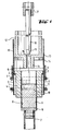
- a tubular crystallization chamber 1 made of, for example, graphite is suspended in the induction heating coil 3 with the water cooling 4 via the holder 2 made of, for example, electrically insulating quartz.
- the additional quartz ring 5 is used only for easier fitting of the upper device components.
- the bottom 6 made of graphite sits on a vertically movable tube 7 made of, for example, quartz, through which a cooling medium, for example air, can flow.
- the thin protective melt film 8 enables the silicon rod 9, which grows crystalline on the cooled plate 6, to be easily removed from the crystallization chamber 1, while from the silicon reservoir of the protruding recharging device 12 made of, for example, graphite, solid or liquid silicon can be tracked in accordance with the crystallization.
- the recharging crucible 12 which is held, for example, by a quartz ring 14 located in a quartz tube piece 13, has in the center a conically downwardly tapering outflow opening 15 which fits into a downwardly positioned guide tube 16 continues.
- This outflow opening 15 can be closed by a suitably also made of graphite and rotatable via the drive shaft 17 and vertically adjustable stopper rod 18, which is also tapered at its lower end 19 to fit and be opened to form an annular gap or entirely.
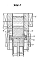
- FIG. 2 in turn shows a crystallization chamber 1 ′ surrounded by a heating device 3 ′ with a silicon rod 9 separated by a protective melt film 8 with a silicon melting lake 11 covered above the crystallization front 10.
- the silicon rod 9 is drawn downwards into a post-heating zone consisting of a resistance heater 20 surrounded graphite tube 21, which is separated by an insulating ring 22 from the crystallization chamber 1 'made of graphite.
- the cooling floor 6 is shielded from the heat radiation of the graphite tube 21 by heat insulation 23 made of, for example, quartz or asbestos.
- the bottom 6 is seated on a double-walled quartz tube 24, into which a liquid or gaseous cooling medium is brought through a central tube 25 directly to the underside of the cooling base 6 and from there flows out again via the double wall.
- the vertically movable base had a thickness of 5 mm and, like the crystallization chamber, was made of graphite, and the graphite parts were also impregnated in equal parts by immersion in a protective melt of calcium silicate (CaSi0 3 ) and calcium fluoride (CaF 2 ).
- the induction heating was adjusted in such a way that a temperature of approximately 1450 ° C. prevailed at the upper edge of the chamber, which dropped to approximately 1350 ° C. towards the bottom.
- the silicon began to crystallize out like a stem on the base plate, which was seated on a quartz tube, whereupon the base plate was pulled down at a rate of initially 10 mm / minute to finally 25 mm / minute, the rod part emerging from the crystallization chamber being exposed to the surrounding atmosphere was cooled.
- the height of the melting lake was adjusted to about 10 mm by recharging during crystal growth.
- the experiment was stopped after about 35 minutes.
- the result was a silicon rod 700 mm long and a cross section of 30 x 30 mm.
- the rod had a columnar structure of single-crystal crystal regions with a preferred orientation (the 111 direction).
- the columnar crystal growth given by the seed crystal continued in the growing solidifying silicon.
- the silicon rod was stripped at an average speed of approximately 20 mm / minute, the rod passing through a post-heating zone of approximately 1350 to 1200 ° C. immediately following the crystallization chamber, in which it was annealed without stress. At the same time it was thereby achieved that the isotherms were flat even at a greater distance from the crystallization front and were almost perpendicular to the direction of removal.
- the silicon rod was further cooled by blowing with nitrogen through a set of nozzles arranged concentrically around the rod.
- a post-charging device made of protective melt-impregnated (CaSiO 3 .CaF 2 ) graphite was used to prepare precleaned molten silicon containing 10 ppm of boron and 1 ppm of phosphorus in addition to about 5% by weight of CaSiO 3 .CaF 2 continuously adjusted in such an amount that a silicon melt pool of about 10 mm in height was maintained in the crystallization chamber.
- the post-charge crucible had a capacity of about 20 liters of silicon melt and 5% by weight of protective melt.
- the silicon rods were then sawn into 400 mm thick slices and further processed into solar cells.
Landscapes
- Chemical & Material Sciences (AREA)
- Engineering & Computer Science (AREA)
- Materials Engineering (AREA)
- Organic Chemistry (AREA)
- Crystallography & Structural Chemistry (AREA)
- Metallurgy (AREA)
- Ceramic Engineering (AREA)
- Manufacturing & Machinery (AREA)
- Structural Engineering (AREA)
- Silicon Compounds (AREA)
- Photovoltaic Devices (AREA)
- Crystals, And After-Treatments Of Crystals (AREA)
- Liquid Deposition Of Substances Of Which Semiconductor Devices Are Composed (AREA)
Claims (7)
Applications Claiming Priority (2)
| Application Number | Priority Date | Filing Date | Title |
|---|---|---|---|
| DE19792925679 DE2925679A1 (de) | 1979-06-26 | 1979-06-26 | Verfahren zur herstellung von siliciumstaeben |
| DE2925679 | 1979-06-26 |
Publications (2)
| Publication Number | Publication Date |
|---|---|
| EP0021385A1 EP0021385A1 (fr) | 1981-01-07 |
| EP0021385B1 true EP0021385B1 (fr) | 1983-05-25 |
Family
ID=6074159
Family Applications (1)
| Application Number | Title | Priority Date | Filing Date |
|---|---|---|---|
| EP80103506A Expired EP0021385B1 (fr) | 1979-06-26 | 1980-06-23 | Procédé de fabrication de barres en silicium |
Country Status (6)
| Country | Link |
|---|---|
| US (1) | US4312700A (fr) |
| EP (1) | EP0021385B1 (fr) |
| JP (1) | JPS5819639B2 (fr) |
| AU (1) | AU534922B2 (fr) |
| CA (1) | CA1155735A (fr) |
| DE (2) | DE2925679A1 (fr) |
Cited By (1)
| Publication number | Priority date | Publication date | Assignee | Title |
|---|---|---|---|---|
| DE102009021003A1 (de) * | 2009-05-12 | 2010-11-18 | Centrotherm Sitec Gmbh | Verfahren und Vorrichtung zur Bereitstellung flüssigen Siliziums |
Families Citing this family (31)
| Publication number | Priority date | Publication date | Assignee | Title |
|---|---|---|---|---|
| NL8005312A (nl) * | 1980-09-24 | 1982-04-16 | Philips Nv | Werkwijze voor het vervaardigen van ferriet eenkristallen. |
| US4400232A (en) * | 1981-11-09 | 1983-08-23 | Eagle-Picher Industries, Inc. | Control of oxygen- and carbon-related crystal defects in silicon processing |
| CA1222436A (fr) * | 1982-08-23 | 1987-06-02 | Franz T. Geyling | Epitaxie de cristaux |
| US4442082A (en) * | 1982-12-27 | 1984-04-10 | Sri International | Process for obtaining silicon from fluosilicic acid |
| US4597948A (en) * | 1982-12-27 | 1986-07-01 | Sri International | Apparatus for obtaining silicon from fluosilicic acid |
| DE3427465A1 (de) * | 1984-07-25 | 1986-01-30 | Heliotronic Forschungs- und Entwicklungsgesellschaft für Solarzellen-Grundstoffe mbH, 8263 Burghausen | Verfahren und vorrichtung zur taktweisen herstellung von siliciumformkoerpern |
| IT1178785B (it) * | 1984-12-21 | 1987-09-16 | Pragma Spa | Procedimento per la preparazione di materiali policristallini ed apparechiatura atta alla sua realizzazione |
| US4593910A (en) * | 1985-03-07 | 1986-06-10 | Commonwealth Of Puerto Rico | Board game |
| DE3531610A1 (de) * | 1985-09-04 | 1987-03-05 | Wacker Chemitronic | Verfahren und vorrichtung zur herstellung von siliciumstaeben |
| JPH0753569B2 (ja) * | 1986-08-07 | 1995-06-07 | 昭和アルミニウム株式会社 | ケイ素の精製方法 |
| US4921026A (en) * | 1988-06-01 | 1990-05-01 | Union Carbide Chemicals And Plastics Company Inc. | Polycrystalline silicon capable of yielding long lifetime single crystalline silicon |
| DE3907916A1 (de) * | 1989-03-11 | 1990-09-13 | Bayer Ag | Vorrichtung zum dosieren von siliciumschmelzen |
| US5135047A (en) * | 1989-10-05 | 1992-08-04 | Flavio Dobran | Furnace for high quality and superconducting bulk crystal growths |
| JP2516823B2 (ja) * | 1990-02-28 | 1996-07-24 | 信越半導体株式会社 | 浮遊帯域融解法による単結晶シリコン製造用の棒状多結晶シリコン及びその製造方法 |
| US5016683A (en) * | 1990-03-27 | 1991-05-21 | General Signal Corporation | Apparatus for controllably feeding a particulate material |
| DE4018967A1 (de) * | 1990-06-13 | 1991-12-19 | Wacker Chemitronic | Verfahren und vorrichtung zum giessen von siliciumbloecken mit kolumnarstruktur als grundmaterial fuer solarzellen |
| DE4323793A1 (de) * | 1993-07-15 | 1995-01-19 | Wacker Chemitronic | Verfahren zur Herstellung von Stäben oder Blöcken aus beim Erstarren sich ausdehnendem Halbleitermaterial durch Kristallisieren einer aus Granulat erzeugten Schmelze sowie Vorrichtung zu seiner Durchführung |
| DE19607098C2 (de) * | 1996-02-24 | 1999-06-17 | Ald Vacuum Techn Gmbh | Verfahren und Vorrichtung zum gerichteten Erstarren einer Schmelze aus Silizium zu einem Block in einem bodenlosen metallischen Kaltwandtiegel |
| US6313398B1 (en) * | 1999-06-24 | 2001-11-06 | Shin-Etsu Chemical Co., Ltd. | Ga-doped multi-crytsalline silicon, Ga-doped multi-crystalline silicon wafer and method for producing the same |
| DE10021585C1 (de) * | 2000-05-04 | 2002-02-28 | Ald Vacuum Techn Ag | Verfahren und Vorrichtung zum Einschmelzen und Erstarren von Metallen und Halbmetallen in einer Kokille |
| KR100370610B1 (ko) * | 2000-09-22 | 2003-01-30 | 성실전자 주식회사 | 고전압 방전 저항체 및 그 제조방법 |
| US8021483B2 (en) * | 2002-02-20 | 2011-09-20 | Hemlock Semiconductor Corporation | Flowable chips and methods for the preparation and use of same, and apparatus for use in the methods |
| NO318092B1 (no) * | 2002-05-22 | 2005-01-31 | Elkem Materials | Kalsium-silikatbasert slagg, fremgangsmate for fremstilling av kalsium-silikatbasert slagg, og anvendelse for slaggbehandling av smeltet silium |
| AU2003277041A1 (en) * | 2002-09-27 | 2004-04-19 | Astropower, Inc. | Methods and systems for purifying elements |
| JP3855082B2 (ja) * | 2002-10-07 | 2006-12-06 | 国立大学法人東京農工大学 | 多結晶シリコンの作製方法、多結晶シリコン、及び太陽電池 |
| NO322246B1 (no) * | 2004-12-27 | 2006-09-04 | Elkem Solar As | Fremgangsmate for fremstilling av rettet storknede silisiumingots |
| US8968467B2 (en) * | 2007-06-27 | 2015-03-03 | Silicor Materials Inc. | Method and system for controlling resistivity in ingots made of compensated feedstock silicon |
| US9580327B2 (en) * | 2014-02-11 | 2017-02-28 | Rec Silicon Inc | Method and apparatus for consolidation of granular silicon and measuring non-metals content |
| US20160230307A1 (en) * | 2015-02-05 | 2016-08-11 | Solarworld Industries America Inc. | Apparatus and methods for producing silicon-ingots |
| EP3156389A1 (fr) * | 2015-10-12 | 2017-04-19 | GFBiochemicals Ltd | Procédé de purification de l'acide lévulinique |
| JP6535928B2 (ja) * | 2016-05-16 | 2019-07-03 | 三菱造船株式会社 | 液化ガスによる急冷可否判定装置、液化ガス貯留タンク、液化ガス運搬船及び液化ガスによる急冷可否判定方法 |
Family Cites Families (9)
| Publication number | Priority date | Publication date | Assignee | Title |
|---|---|---|---|---|
| US2475810A (en) * | 1944-01-05 | 1949-07-12 | Bell Telephone Labor Inc | Preparation of silicon material |
| GB954849A (en) * | 1961-08-04 | 1964-04-08 | Ici Ltd | Production of silicon |
| US3267529A (en) * | 1961-10-04 | 1966-08-23 | Heraeus Gmbh W C | Apparatus for melting metals under high vacuum |
| BE759122A (fr) * | 1969-11-19 | 1971-05-18 | Union Carbide Corp | Procede et charge de production de silicium au four a arc electrique par reduction carbothermique de silice |
| US3745043A (en) * | 1971-05-13 | 1973-07-10 | Union Carbide Corp | Manufacture of silicon metal from dichlorosilane |
| US3759310A (en) * | 1971-08-30 | 1973-09-18 | United Aircraft Corp | Nsumable electrode method and apparatus for providing single crystal castings using a co |
| DE2722784A1 (de) * | 1977-05-20 | 1978-11-30 | Wacker Chemitronic | Verfahren zum reinigen von feststoffen |
| DE2745247C3 (de) * | 1977-10-07 | 1980-03-13 | Wacker-Chemitronic Gesellschaft Fuer Elektronik-Grundstoffe Mbh, 8263 Burghausen | Verfahren und Vorrichtung zur semikontinuierlichen Herstellung von Siliciumformkörpern |
| DE2845459A1 (de) * | 1978-10-19 | 1980-04-30 | Consortium Elektrochem Ind | Verfahren zum schutz von kohlenstoffkoerpern |
-
1979
- 1979-06-26 DE DE19792925679 patent/DE2925679A1/de not_active Withdrawn
-
1980
- 1980-06-03 JP JP55073826A patent/JPS5819639B2/ja not_active Expired
- 1980-06-09 US US06/157,707 patent/US4312700A/en not_active Expired - Lifetime
- 1980-06-11 CA CA000353782A patent/CA1155735A/fr not_active Expired
- 1980-06-23 EP EP80103506A patent/EP0021385B1/fr not_active Expired
- 1980-06-23 DE DE8080103506T patent/DE3063462D1/de not_active Expired
- 1980-06-25 AU AU59589/80A patent/AU534922B2/en not_active Ceased
Cited By (1)
| Publication number | Priority date | Publication date | Assignee | Title |
|---|---|---|---|---|
| DE102009021003A1 (de) * | 2009-05-12 | 2010-11-18 | Centrotherm Sitec Gmbh | Verfahren und Vorrichtung zur Bereitstellung flüssigen Siliziums |
Also Published As
| Publication number | Publication date |
|---|---|
| JPS565399A (en) | 1981-01-20 |
| AU534922B2 (en) | 1984-02-23 |
| JPS5819639B2 (ja) | 1983-04-19 |
| DE2925679A1 (de) | 1981-01-22 |
| AU5958980A (en) | 1981-01-08 |
| DE3063462D1 (en) | 1983-07-07 |
| EP0021385A1 (fr) | 1981-01-07 |
| CA1155735A (fr) | 1983-10-25 |
| US4312700A (en) | 1982-01-26 |
Similar Documents
| Publication | Publication Date | Title |
|---|---|---|
| EP0021385B1 (fr) | Procédé de fabrication de barres en silicium | |
| DE69932760T2 (de) | Verfahren und Vorrichtung zur Herstellung eines Siliciumstabes mit einer Struktur hergestellt durch gerichtete Erstarrung | |
| EP0072565B1 (fr) | Procédé de fabrication de rubans macro- à monocristallins en matériau semi-conducteur | |
| EP0013985B1 (fr) | Procédé de fabrication de feuilles de silicium cristallin à gros grains avec orientation préférentielle | |
| EP2028292B1 (fr) | Procédé de fabrication de corps métallique ou semi-métalliques monocristallins | |
| DE2508803C3 (de) | Verfahren zur Herstellung plattenförmiger Siliciumkristalle mit Kolumnarstruktur | |
| DE68913237T2 (de) | Siliciumgiessvorrichtung. | |
| DE4018967A1 (de) | Verfahren und vorrichtung zum giessen von siliciumbloecken mit kolumnarstruktur als grundmaterial fuer solarzellen | |
| DE102006017622A1 (de) | Verfahren und Vorrichtung zur Herstellung von multikristallinem Silizium | |
| EP0217158A2 (fr) | Procédé et appareil pour la fabrication de barreaux de silicium | |
| DE4323793A1 (de) | Verfahren zur Herstellung von Stäben oder Blöcken aus beim Erstarren sich ausdehnendem Halbleitermaterial durch Kristallisieren einer aus Granulat erzeugten Schmelze sowie Vorrichtung zu seiner Durchführung | |
| EP0172426B1 (fr) | Procédé et appareil pour la préparation par étapes de produits en silicium | |
| DE2548046A1 (de) | Verfahren zur herstellung einkristalliner siliciumstaebe | |
| DE69528051T2 (de) | Kristallwachstumsverfahren | |
| DE19922736C2 (de) | Vorrichtung zum Herstellen eines Einkristalls | |
| DE112021005126B4 (de) | Herstellungsverfahren für Silicium-Einkristall | |
| EP0120395B1 (fr) | Méthode pour fabriquer du silicium macrocristallin | |
| WO1990004054A1 (fr) | Procede et dispositif de tirage de cristaux selon la methode de czochralski | |
| DE2142388A1 (de) | Verfahren zum Herstellen von kristallinen Körpern aus III-V-Halbleiterverbindungen | |
| DE3107596A1 (de) | "verfahren zur herstellung von halbleiterscheiben" | |
| DE3220285A1 (de) | Verfahren zum herstellen polykristalliner, fuer nachfolgendes zonenschmelzen geeigneter siliciumstaebe | |
| DE68912686T2 (de) | Verfahren zur Herstellung eines Einkristalls aus einer Halbleiter-Verbindung. | |
| DE3210827C2 (de) | Verfahren zum Züchten eines III/V-Verbindungs-Einkristalls | |
| DE3220343A1 (de) | Verfahren zum herstellen polykristalliner siliciumstaebe | |
| DE1196625B (de) | Verfahren zur Herstellung von einkristallinem Siliciumkarbid |
Legal Events
| Date | Code | Title | Description |
|---|---|---|---|
| PUAI | Public reference made under article 153(3) epc to a published international application that has entered the european phase |
Free format text: ORIGINAL CODE: 0009012 |
|
| 17P | Request for examination filed |
Effective date: 19801023 |
|
| AK | Designated contracting states |
Designated state(s): BE DE FR GB IT NL |
|
| ITF | It: translation for a ep patent filed | ||
| GRAA | (expected) grant |
Free format text: ORIGINAL CODE: 0009210 |
|
| AK | Designated contracting states |
Designated state(s): BE DE FR GB IT NL |
|
| REF | Corresponds to: |
Ref document number: 3063462 Country of ref document: DE Date of ref document: 19830707 |
|
| ET | Fr: translation filed | ||
| PLBE | No opposition filed within time limit |
Free format text: ORIGINAL CODE: 0009261 |
|
| STAA | Information on the status of an ep patent application or granted ep patent |
Free format text: STATUS: NO OPPOSITION FILED WITHIN TIME LIMIT |
|
| PGFP | Annual fee paid to national office [announced via postgrant information from national office to epo] |
Ref country code: FR Payment date: 19840517 Year of fee payment: 5 |
|
| PGFP | Annual fee paid to national office [announced via postgrant information from national office to epo] |
Ref country code: DE Payment date: 19840530 Year of fee payment: 5 |
|
| 26N | No opposition filed | ||
| PGFP | Annual fee paid to national office [announced via postgrant information from national office to epo] |
Ref country code: BE Payment date: 19840630 Year of fee payment: 5 |
|
| PGFP | Annual fee paid to national office [announced via postgrant information from national office to epo] |
Ref country code: NL Payment date: 19870630 Year of fee payment: 8 |
|
| PG25 | Lapsed in a contracting state [announced via postgrant information from national office to epo] |
Ref country code: GB Effective date: 19880623 |
|
| BERE | Be: lapsed |
Owner name: HELIOTRONIC FORSCHUNGS- UND ENTWICKLUNGS G. FUR S Effective date: 19880630 |
|
| PG25 | Lapsed in a contracting state [announced via postgrant information from national office to epo] |
Ref country code: NL Effective date: 19890101 |
|
| NLV4 | Nl: lapsed or anulled due to non-payment of the annual fee | ||
| GBPC | Gb: european patent ceased through non-payment of renewal fee | ||
| PG25 | Lapsed in a contracting state [announced via postgrant information from national office to epo] |
Ref country code: FR Free format text: LAPSE BECAUSE OF NON-PAYMENT OF DUE FEES Effective date: 19890228 |
|
| PG25 | Lapsed in a contracting state [announced via postgrant information from national office to epo] |
Ref country code: DE Effective date: 19890301 |
|
| REG | Reference to a national code |
Ref country code: FR Ref legal event code: ST |
|
| PG25 | Lapsed in a contracting state [announced via postgrant information from national office to epo] |
Ref country code: BE Effective date: 19890630 |