EP0023429A2 - Trockene Ätzung eines metallischen Films - Google Patents
Trockene Ätzung eines metallischen Films Download PDFInfo
- Publication number
- EP0023429A2 EP0023429A2 EP80302564A EP80302564A EP0023429A2 EP 0023429 A2 EP0023429 A2 EP 0023429A2 EP 80302564 A EP80302564 A EP 80302564A EP 80302564 A EP80302564 A EP 80302564A EP 0023429 A2 EP0023429 A2 EP 0023429A2
- Authority
- EP
- European Patent Office
- Prior art keywords
- film
- aluminum
- metal film
- etchant gas
- gas
- Prior art date
- Legal status (The legal status is an assumption and is not a legal conclusion. Google has not performed a legal analysis and makes no representation as to the accuracy of the status listed.)
- Granted
Links
Images






Classifications
-
- H—ELECTRICITY
- H10—SEMICONDUCTOR DEVICES; ELECTRIC SOLID-STATE DEVICES NOT OTHERWISE PROVIDED FOR
- H10P—GENERIC PROCESSES OR APPARATUS FOR THE MANUFACTURE OR TREATMENT OF DEVICES COVERED BY CLASS H10
- H10P70/00—Cleaning of wafers, substrates or parts of devices
- H10P70/20—Cleaning during device manufacture
- H10P70/27—Cleaning during device manufacture during, before or after processing of conductive materials, e.g. polysilicon or amorphous silicon layers
- H10P70/273—Cleaning during device manufacture during, before or after processing of conductive materials, e.g. polysilicon or amorphous silicon layers the processing being a delineation of conductive layers, e.g. by RIE
-
- C—CHEMISTRY; METALLURGY
- C23—COATING METALLIC MATERIAL; COATING MATERIAL WITH METALLIC MATERIAL; CHEMICAL SURFACE TREATMENT; DIFFUSION TREATMENT OF METALLIC MATERIAL; COATING BY VACUUM EVAPORATION, BY SPUTTERING, BY ION IMPLANTATION OR BY CHEMICAL VAPOUR DEPOSITION, IN GENERAL; INHIBITING CORROSION OF METALLIC MATERIAL OR INCRUSTATION IN GENERAL
- C23F—NON-MECHANICAL REMOVAL OF METALLIC MATERIAL FROM SURFACE; INHIBITING CORROSION OF METALLIC MATERIAL OR INCRUSTATION IN GENERAL; MULTI-STEP PROCESSES FOR SURFACE TREATMENT OF METALLIC MATERIAL INVOLVING AT LEAST ONE PROCESS PROVIDED FOR IN CLASS C23 AND AT LEAST ONE PROCESS COVERED BY SUBCLASS C21D OR C22F OR CLASS C25
- C23F4/00—Processes for removing metallic material from surfaces, not provided for in group C23F1/00 or C23F3/00
Definitions
- the present invention relates to dry etching, more particularly to a process for the dry etching of a metal film which comprises aluminum as a main component and is provided on a semiconductor chip.
- Materials of a conductor pattern of a semiconductor device are generally aluminum and aluminum based metal including aluminum-copper, aluminum-silicon and aluminum-copper-silicon.
- the addition of copper to aluminum increases its electromigration resistance and the addition of silicon to aluminum prevents silicon depletion of shallow junctions.
- dry etching i.e. plasuma etching, reactive ion etching and reactive sputter etching
- wet chemical etching for several reasons.
- dry etching is cleaner, results in a smaller linewidth of the pattern, i.e. a film pattern, there are no noxious and polluting acids and solvents involved, and it is more economic than wet etching.
- Some etchant gases for example, the following three kinds of gases have been proposed for the dry etching of an aluminum film and an aluminum based film.
- aluminum residue which is aluminum oxide, tends to remain.
- AlC1 3 aluminum trichloride
- the copper compound of the film is volatile only at temperatures above 1000°C and, since the temperature does not exceed 150°C during the etching period, volatilizing of the copper compound does not occur.
- copper residues accumulate during the dry etching and prevent further etching, it is difficult to etch an aluminum-copper film.
- This mixed gas (PCl 3 +BC1 3 ) has the ability to cause chemical sputtering of a metal film to be etched and, therefore, it is possible to etch an aluminum film and an aluminum-copper film, and simultaniously, to remove aluminum residues and copper residues.
- phosphorus trichloride has strong corrosion tendency, easily reacts with moisture in the air to produce hydrochloric acid (HC1) and is labile.
- the permissible concentration range of the phosphorus trichloride is very narrow and depends on the dry etching conditions, such as the pressure inside the vaccum system, the power of the etching apparatus and the total pressure of the mixed gas.
- the concentration of the phosphorus trichloride is outside the permissible range, satisfactory etching can not be performed.
- the mixed gas tends to undercut a masking film (i.e. a patterned photoresist film), namely, the etchant gas horizontally etches a portion of the aluminum or aluminum based film which is covered with the masking film.
- the aluminum etchrate i.e. etching rate
- the aluminum etchrate is small, since the number of generated chloric radicals is small.
- the addition of oxygen to the boron trichloride increases the number of the generated chloric radicals, so that the aluminum etchrate increases, but undesirable undercutting occurs.
- the proposed etchant gases has demerits.
- a fluorine gas being one of halogen gases as the etchant gas.
- a fluorine gas being one of halogen gases
- an aluminum fluoride film is gradually formed, since the aluminum fluoride is not volatile at temperatures under 1260°C.
- the aluminum fluoride film serves as a possive film, so that further etching progress is not made.
- An object of the present invention is to provide a dry etching process wherein a new etchant gas for etching an aluminum film and an aluminum based film is used.
- Another object of the present invention is to provide a process for dry etching an aluminum film and an aluminum based film at relatively high etchrates.
- a further object of the present invention is to form a fine conductor pattern of aluminum or aluminum based metal on a semiconductor chip.
- a process for dry etching a metal film having aluminum as a main component which comprises the step of exposing the metal film to an etchant gas having as a principal ingredient a mixed gas of carbon chloride (e.g. carbon tetrachloride) and boron chloride (e.g. boron trichloride).
- a mixed gas of carbon chloride e.g. carbon tetrachloride
- boron chloride e.g. boron trichloride
- the partial pressure of the carbon tetrachloride is in the range of from 30 to 80 percent of the total pressure of the mixed gas that the etchant gas has a pressure in the range of from 100 to 250 milli-Torr.
- High purity aluminum was etched in a conventional plasma etching apparatus under the following conditions, wherein the mixing ratio of each etchant gas was varied.
- Fig. 1 The results of the Experiment 1 are shown in Fig. 1, wherein the ordinate indicates the aluminum etchrate, and the abscissa indicates the ratio of partical pressure of CC1 4 or PCI 3 to the total pressure (200 milli-Torr) of the etchant gas.
- the aluminum etchrate obtained by using the etchant gas (mixed gas) of CC1 4 and BC1 3 was higher than that obtained by using the mixed gas of PC1 3 and BC1 3 or the mixed gas of CC1 4 and He.
- High purity aluminum was etched in the plasma etching apparatus used in the Experiment 1 under the following conditions, wherein the RF power was varied.
- High purity aluminum was etched in the plasma etching apparatus used in the Experiment 1 under the following conditions, wherein the total pressure of the each etchant gas was varied.
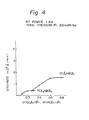
- Aluminum-copper (4 wt%) metal was etched in the plasma etching apparatus used in the Experiment 1 under the following conditions, wherein the mixing ratio of each etchant gas was varied.
- the results of the Experiment 4 are shown in Fig. 4.
- the aluminum-copper metal etchrate obtained by using the etchant gas of CC1 4 and BC1 3 was higher than that obtained by using the etchant gas of PC1 3 and BC1 3 .
- Etching condition B (a comparative example) Etchant gas: CC1 4 + He
- the silicon was a (100) oriented single crystalline silicon
- the negative type photoresist was OMR-83 (a product of TOKYO OHKA KOGYO) and the silicon dioxide was produced by thermal oxidizing silicon.
- the etchrates of the silicon and photoresist obtained under the etching condition A were lower than those obtained in both the etching conditions B and C. Namely, the selective etching ablility of the etchant gas of CC1 4 and BCl 3 under the etching condition A is superior to that of the etchant gases under the etching conditions B and C.
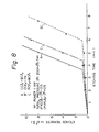
- etching conditions were that the RF power was 1KW and the ratio of partial pressuer of CC1 4 or PC1 3 to the total pressure of each of the etchant gases was 0.5.
- the aluminum etchrate was measured at three points a, b and c of the aluminum film, having a diameter of 3 inches, after the dry etching.
- the point b was the center of the aluminum film, and the points a and c were at a distance of approximetly 2.9 mm from the center point b, while the points a, b and c were in a straigh line.
- the aluminum etchrate was measured at the three points a, b and c of the aluminum film, which were the same points as explained in Experiment 6.
- a structure of specimens to be etched consisted of a silicon single crystalline wafer, a silicon dioxide (Si0 2 ) film having a thickness of 4000 angstroms (A), a high purity aluminum film having a thickness of 10000 angstroms and an aluminum oxide (AlO x , wherein x was in the range of 1 through 2) film having a thickness of 900 angstroms.
- the silicon dioxide film was formed by thermal oxidizing the surface of the silicon wafer and the aluminum film was formed on the silicon dioxide film by vacuum evaporation. Then, the aluminum film was oxidized by anodic oxidation to form the aluminum oxide film comprised of A1 2 0 3 .
- the specimens having the above-mentioned structure were etched in the plasma etching apparatus used in the Experiment 1 under the following three conditions A, B' and C.
- the Etching Conditions A and C were the same as the Etching Conditions A and C in Experiment 5, respectively.
- the etching condition B' was the same as the Etching Condition B in the Experiment 5, except that the partial pressure ratio of CCl 4 was 0.5.
- the aluminum oxide layer can be etched most rapidly in the etching condition A among the three etching conditions.
- the etchant gas of CC1 4 and BC1 3 can etch more rapidly than both the etchant gas of PC1 3 and BC1 3 and the etchant gas of CC1 4 and He.
- samples to be etched were produced in the following manner.
- the same type of silicon single crystalline wafer as used in the Experiment 8 was thermal oxidized to form a silicon dioxide (Si0 2 ) film having a thickness of 4000 angstroms.
- a metal film of aluminum or aluminum-4 wt% copper having a thickness of 1 micron-meter was formed by vaccum evaporation.
- a negative type photoresist (OMR-83) having a thickness of approximately 1 micron-meter was applied on the metal film, exposed and developed to form a predetermined masking pattern.
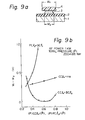
- the obtained samples were etched attain 50% overetching in the plasma etching apparatus used in the Experiment 1 under the following conditions, wherein the mixing ratio of each etchant gas was varied.
- FIG. 9a A portion of one of the overetched samples is illustrated in the sectional view of Fig. 9a.
- a silicon dioxide film 2 is on top of a silicon wafer 1
- an etched metal film 3 is on top of the silicon dioxide film 2
- a patterned photoresist 4 is on top of the metal film 3.
- An amount of overetching is defined as W minus W 2 , wherein W 2 is a width of a conductor line of the overetched metal film 3 and W 1 is a width of a line of the patterned photoresist 4.
- the use of the mixed gas of CC1 4 and BC1 3 as an etchant gas is preferable to the use of the mixed gas of PC1 3 and BC1 3 and the mixed gas of CC1 4 and He.
- the gases of CC1 4 and BC1 3 for the etchant gas of the present invention were introduced into a reaction chamber of the etching'apparatus without a carrier gas, respectively.
- an inert gas Ar or He
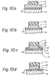
- an aluminum film 11 is formed by vacuum evaporation or any other suitable technique on the surface of a semiconductor chip 12.
- the semiconductor chip 12 comprises a semiconductor substrate 13, e.g. a silicon single crystalline wafer, and an insulating film 14, e.g. a silicon dioxide film, which covers the surface of the substrate 13.
- a photoresist masking film 15 is applied on the surface of the aluminum film 11, exposed and developed to form a predetermined pattern, as illustrated in Fig. 10a.
- the aluminum film 11 on the semiconductor chip 12 is selectively etched in a dry etching apparatus, e.g.
- the mixed gas CC1 4 and BC1 3 as the etchant gas to remove one-half to three-fourths of the unmasked portion of the aluminum film 11, as illustrated in Fig. 10b.
- the etchant gas consist of CC1 4 and BCl 3 , but it is possible to add an inert gas, i.e. Ar or He, to the mixed gas of CCI 4 and BC1 3 .
- a preferred partial pressure of the inert gas is less than 60 percent of the total pressure.
- the semiconductor chip 12 is, then, taken out of the etching apparatus, and is treated with water, namely, is washed with water or is placed in a boiling water bath, to form an aluminum oxide film 16 comprising of Al203 on the exposed surface of the aluminum film 11, as illustrated in Fig. 10c.
- a preferred thickness of the aluminum oxide film 16 is in the range of 100 to 1000 angstroms.
- the aluminum film 11 with the aluminum oxide film 16 is reetched in the same etching apparatus by using the mixed gas of CC1 4 and BC1 3 .
- the etchrate of a horizontal protion 16' of the aluminum oxide film 16 is higher than that of a vertical portion 16" thereof, since a generated chemical sputtering effect of the horizontal portion 16' is stronger than that of the vertical portion 16".
- the aluminum etchrate is higher than the aluminum oxide etchrate, the portion of aluminum film which is not covered with the photoresist 15 is removed, as illustrated in Fig. 10d. Accordingly, it is possible to obtain a conductor pattern of aluminum without undercutting or with very small undercutting.
- an aluminum based film 21 of either aluminum-copper or aluminum-silicon is formed on the surface of a semiconductor chip 22 by vacuum evaporation or any other suitable technique.
- the semiconductor chip 22 comprises a semiconductor substrate 23 and an insulating film 24, which are the same as the semiconductor substrate 13 and the insulating film 14, respectively.
- a photoresist masking film 25 is applied on the surface of the aluminum based metal 21, exposed and developed to form a pattern, as illustrated in Fig. lla.
- the aluminum based film 21 is selectively etched in a plasma etching apparatus or a reactive ion etching apparatus by using the mixed gas of CC1 4 and BCI 3 to remove one-half to three-fourths of the unmasked portion of the aluminum film 21, as illustrated in Fig. llb. After this etching, copper or silicon residues 27 remain on the etched aluminum based metal 21.
- the semiconductor chip 22 is taken out the etching apparatus and, then, the copper or silicon residues 27 are removed by nitric acid (HN0 3 ) solution or carbon tetrafluoride and oxygen (CF 4 +5%O 2 ) plasma which is generated under a condition, e.g. at 0.5 Torr, 500 watts, for 1 minute. Thereafter, the exposed surface of the aluminum based film 21 is washed with water. Such treatment in water forms an aluminum oxide (AlO ) film 26 on the exposed surface of the aluminum based film 21, as illustrated in Fig. llc. A preferred thickness of the aluminum oxide film 26 is in the range of from 100 to 300 angstroms.
- the aluminum based film 21 with the aluminum oxide film 26 consisting of a horizontal portion 26' and a vertical portion 26" is reetched in the same etching apparatus by using the mixed gas of CC1 4 and BC1 - . Since the reetching preceeds in the same manner as the above--mentined reetching of the aluminum film, the portion of aluminum based film 21 which is not covered with the photoresist 25 is removed, as shown in Fig. lld. Accordingly, it is possible to obtain a conductor pattern of aluminum-copper or aluminum-silicon without undercutting or with very small undercutting.
Landscapes
- Chemical & Material Sciences (AREA)
- Engineering & Computer Science (AREA)
- Materials Engineering (AREA)
- Mechanical Engineering (AREA)
- Metallurgy (AREA)
- Organic Chemistry (AREA)
- Drying Of Semiconductors (AREA)
- Internal Circuitry In Semiconductor Integrated Circuit Devices (AREA)
Applications Claiming Priority (6)
| Application Number | Priority Date | Filing Date | Title |
|---|---|---|---|
| JP98202/79 | 1979-07-31 | ||
| JP98201/79 | 1979-07-31 | ||
| JP9820279A JPS5623277A (en) | 1979-07-31 | 1979-07-31 | Dry etching method |
| JP9820179A JPS5623276A (en) | 1979-07-31 | 1979-07-31 | Dry etching method |
| JP9820379A JPS5623278A (en) | 1979-07-31 | 1979-07-31 | Dry etching method |
| JP98203/79 | 1979-07-31 |
Publications (3)
| Publication Number | Publication Date |
|---|---|
| EP0023429A2 true EP0023429A2 (de) | 1981-02-04 |
| EP0023429A3 EP0023429A3 (en) | 1982-09-08 |
| EP0023429B1 EP0023429B1 (de) | 1985-12-18 |
Family
ID=27308609
Family Applications (1)
| Application Number | Title | Priority Date | Filing Date |
|---|---|---|---|
| EP80302564A Expired EP0023429B1 (de) | 1979-07-31 | 1980-07-28 | Trockene Ätzung eines metallischen Films |
Country Status (5)
| Country | Link |
|---|---|
| US (1) | US4350563A (de) |
| EP (1) | EP0023429B1 (de) |
| CA (1) | CA1136525A (de) |
| DE (1) | DE3071299D1 (de) |
| IE (1) | IE50996B1 (de) |
Cited By (5)
| Publication number | Priority date | Publication date | Assignee | Title |
|---|---|---|---|---|
| EP0122776A3 (en) * | 1983-04-13 | 1987-09-23 | Fujitsu Limited | Dry etching aluminum or aluminum alloy layer |
| US10461078B2 (en) | 2018-02-26 | 2019-10-29 | Taiwan Semiconductor Manufacturing Co., Ltd. | Creating devices with multiple threshold voltage by cut-metal-gate process |
| US11121138B1 (en) | 2020-04-24 | 2021-09-14 | Taiwan Semiconductor Manufacturing Co., Ltd. | Low resistance pickup cells for SRAM |
| US11374088B2 (en) | 2020-08-14 | 2022-06-28 | Taiwan Semiconductor Manufacturing Co., Ltd. | Leakage reduction in gate-all-around devices |
| US11482518B2 (en) | 2021-03-26 | 2022-10-25 | Taiwan Semiconductor Manufacturing Co., Ltd. | Semiconductor structures having wells with protruding sections for pickup cells |
Families Citing this family (29)
| Publication number | Priority date | Publication date | Assignee | Title |
|---|---|---|---|---|
| US4444618A (en) * | 1983-03-03 | 1984-04-24 | General Electric Company | Processes and gas mixtures for the reactive ion etching of aluminum and aluminum alloys |
| US4547261A (en) * | 1984-09-28 | 1985-10-15 | Rca Corporation | Anisotropic etching of aluminum |
| US5221423A (en) * | 1986-05-20 | 1993-06-22 | Fujitsu Limited | Process for cleaning surface of semiconductor substrate |
| JPH03156927A (ja) * | 1989-10-24 | 1991-07-04 | Hewlett Packard Co <Hp> | アルミ・メタライゼーションのパターン形成方法 |
| US5106471A (en) * | 1990-04-02 | 1992-04-21 | Motorola, Inc. | Reactive ion etch process for surface acoustic wave (SAW) device fabrication |
| US5387556A (en) * | 1993-02-24 | 1995-02-07 | Applied Materials, Inc. | Etching aluminum and its alloys using HC1, C1-containing etchant and N.sub.2 |
| US5624868A (en) * | 1994-04-15 | 1997-04-29 | Micron Technology, Inc. | Techniques for improving adhesion of silicon dioxide to titanium |
| US6090717A (en) * | 1996-03-26 | 2000-07-18 | Lam Research Corporation | High density plasma etching of metallization layer using chlorine and nitrogen |
| US5811358A (en) * | 1997-01-03 | 1998-09-22 | Mosel Vitelic Inc. | Low temperature dry process for stripping photoresist after high dose ion implantation |
| US5849641A (en) * | 1997-03-19 | 1998-12-15 | Lam Research Corporation | Methods and apparatus for etching a conductive layer to improve yield |
| US6958295B1 (en) * | 1998-01-20 | 2005-10-25 | Tegal Corporation | Method for using a hard mask for critical dimension growth containment |
| US6391724B1 (en) * | 1999-12-24 | 2002-05-21 | Hyundai Electronics Industries Co., Ltd. | Method for manufacturing a gate structure incorporating aluminum oxide as a gate dielectric |
| JP4213871B2 (ja) * | 2001-02-01 | 2009-01-21 | 株式会社日立製作所 | 半導体装置の製造方法 |
| US20030003374A1 (en) * | 2001-06-15 | 2003-01-02 | Applied Materials, Inc. | Etch process for photolithographic reticle manufacturing with improved etch bias |
| WO2003021659A1 (en) | 2001-09-04 | 2003-03-13 | Applied Materials, Inc. | Methods and apparatus for etching metal layers on substrates |
| TW548862B (en) * | 2002-05-30 | 2003-08-21 | Au Optronics Corp | Method of preventing anode of active matrix organic light emitting diode from breaking |
| WO2004086143A2 (en) * | 2003-03-21 | 2004-10-07 | Applied Materials, Inc. | Multi-step process for etching photomasks |
| US7077973B2 (en) * | 2003-04-18 | 2006-07-18 | Applied Materials, Inc. | Methods for substrate orientation |
| KR100541152B1 (ko) * | 2003-07-18 | 2006-01-11 | 매그나칩 반도체 유한회사 | 반도체 소자의 금속 배선층 형성 방법 |
| US7521000B2 (en) * | 2003-08-28 | 2009-04-21 | Applied Materials, Inc. | Process for etching photomasks |
| US20050279453A1 (en) * | 2004-06-17 | 2005-12-22 | Uvtech Systems, Inc. | System and methods for surface cleaning |
| US7829243B2 (en) * | 2005-01-27 | 2010-11-09 | Applied Materials, Inc. | Method for plasma etching a chromium layer suitable for photomask fabrication |
| KR100944846B1 (ko) * | 2006-10-30 | 2010-03-04 | 어플라이드 머티어리얼스, 인코포레이티드 | 마스크 에칭 프로세스 |
| US8500913B2 (en) * | 2007-09-06 | 2013-08-06 | Micron Technology, Inc. | Methods for treating surfaces, and methods for removing one or more materials from surfaces |
| US9051655B2 (en) | 2013-09-16 | 2015-06-09 | Applied Materials, Inc. | Boron ionization for aluminum oxide etch enhancement |
| US9275800B2 (en) * | 2013-12-19 | 2016-03-01 | Pacesetter, Inc. | Method of nano-patterning a foil surce |
| US10535654B2 (en) | 2017-08-30 | 2020-01-14 | Taiwan Semiconductor Manufacturing Co., Ltd. | Cut metal gate with slanted sidewalls |
| US11043595B2 (en) | 2019-06-14 | 2021-06-22 | Taiwan Semiconductor Manufacturing Co., Ltd. | Cut metal gate in memory macro edge and middle strap |
| US11211116B2 (en) | 2019-09-27 | 2021-12-28 | Taiwan Semiconductor Manufacturing Co., Ltd. | Embedded SRAM write assist circuit |
Family Cites Families (5)
| Publication number | Priority date | Publication date | Assignee | Title |
|---|---|---|---|---|
| US3971684A (en) * | 1973-12-03 | 1976-07-27 | Hewlett-Packard Company | Etching thin film circuits and semiconductor chips |
| US3994793A (en) * | 1975-05-22 | 1976-11-30 | International Business Machines Corporation | Reactive ion etching of aluminum |
| US4030967A (en) * | 1976-08-16 | 1977-06-21 | Northern Telecom Limited | Gaseous plasma etching of aluminum and aluminum oxide |
| JPS54158343A (en) * | 1978-06-05 | 1979-12-14 | Hitachi Ltd | Dry etching method for al and al alloy |
| US4208241A (en) * | 1978-07-31 | 1980-06-17 | Bell Telephone Laboratories, Incorporated | Device fabrication by plasma etching |
-
1980
- 1980-07-28 DE DE8080302564T patent/DE3071299D1/de not_active Expired
- 1980-07-28 EP EP80302564A patent/EP0023429B1/de not_active Expired
- 1980-07-29 CA CA000357204A patent/CA1136525A/en not_active Expired
- 1980-07-30 IE IE1592/80A patent/IE50996B1/en not_active IP Right Cessation
- 1980-07-31 US US06/174,140 patent/US4350563A/en not_active Expired - Lifetime
Cited By (9)
| Publication number | Priority date | Publication date | Assignee | Title |
|---|---|---|---|---|
| EP0122776A3 (en) * | 1983-04-13 | 1987-09-23 | Fujitsu Limited | Dry etching aluminum or aluminum alloy layer |
| US10461078B2 (en) | 2018-02-26 | 2019-10-29 | Taiwan Semiconductor Manufacturing Co., Ltd. | Creating devices with multiple threshold voltage by cut-metal-gate process |
| US10868003B2 (en) | 2018-02-26 | 2020-12-15 | Taiwan Semiconductor Manufacturing Co., Ltd. | Creating devices with multiple threshold voltages by cut-metal-gate process |
| US11121138B1 (en) | 2020-04-24 | 2021-09-14 | Taiwan Semiconductor Manufacturing Co., Ltd. | Low resistance pickup cells for SRAM |
| US11374088B2 (en) | 2020-08-14 | 2022-06-28 | Taiwan Semiconductor Manufacturing Co., Ltd. | Leakage reduction in gate-all-around devices |
| US12266686B2 (en) | 2020-08-14 | 2025-04-01 | Taiwan Semiconductor Manufacturing Co., Ltd. | Leakage reduction in gate-all-around devices |
| US11482518B2 (en) | 2021-03-26 | 2022-10-25 | Taiwan Semiconductor Manufacturing Co., Ltd. | Semiconductor structures having wells with protruding sections for pickup cells |
| US11721687B2 (en) | 2021-03-26 | 2023-08-08 | Taiwan Semiconductor Manufacturing Co., Ltd. | Semiconductor structures having wells with protruding sections for pickup cells |
| US12288784B2 (en) | 2021-03-26 | 2025-04-29 | Taiwan Semiconductor Manufacturing Co., Ltd. | Semiconductor structures having wells with protruding sections for pickup cells |
Also Published As
| Publication number | Publication date |
|---|---|
| CA1136525A (en) | 1982-11-30 |
| DE3071299D1 (en) | 1986-01-30 |
| EP0023429A3 (en) | 1982-09-08 |
| US4350563A (en) | 1982-09-21 |
| EP0023429B1 (de) | 1985-12-18 |
| IE801592L (en) | 1981-01-31 |
| IE50996B1 (en) | 1986-09-03 |
Similar Documents
| Publication | Publication Date | Title |
|---|---|---|
| EP0023429B1 (de) | Trockene Ätzung eines metallischen Films | |
| US4919748A (en) | Method for tapered etching | |
| US5885903A (en) | Process for selectively etching silicon nitride in the presence of silicon oxide | |
| KR940000913B1 (ko) | 플라즈마 에칭에 관한 원상태 포토레지스트의 캡핑방법 | |
| EP0482519B1 (de) | Ätzverfahren für Materialien aus Oxid | |
| US4568410A (en) | Selective plasma etching of silicon nitride in the presence of silicon oxide | |
| US5384009A (en) | Plasma etching using xenon | |
| US5015331A (en) | Method of plasma etching with parallel plate reactor having a grid | |
| EP0122776A2 (de) | Trockenätzen von Schichten aus Aluminium oder aus einer Aluminiumlegierung | |
| US6017826A (en) | Chlorine containing plasma etch method with enhanced sidewall passivation and attenuated microloading effect | |
| EP0350997A2 (de) | Reaktives Ionenätzen von Silicium enthaltenden Materialien mittels Bromwasserstoff | |
| US4615764A (en) | SF6/nitriding gas/oxidizer plasma etch system | |
| IE55419B1 (en) | Plasma reactive ion etching of aluminum and aluminum alloys | |
| EP0036144A1 (de) | Verfahren zum selektiven reaktiven Ionenätzen von Silicium | |
| US6008137A (en) | Pattern formation of silicon nitride | |
| JP2903884B2 (ja) | 半導体装置の製法 | |
| US5522520A (en) | Method for forming an interconnection in a semiconductor device | |
| US5387312A (en) | High selective nitride etch | |
| US6057240A (en) | Aqueous surfactant solution method for stripping metal plasma etch deposited oxidized metal impregnated polymer residue layers from patterned metal layers | |
| EP1235265A1 (de) | Verfahren zum Ätzen einer harten Maskeschicht und einer Metallschicht | |
| EP0485802B1 (de) | Verfahren zur Korrosionsverhinderung von Aluminiumlegierungen | |
| US5126008A (en) | Corrosion-free aluminum etching process for fabricating an integrated circuit structure | |
| US4364793A (en) | Method of etching silicon and polysilicon substrates | |
| US6069087A (en) | Highly selective dry etching process | |
| US5338395A (en) | Method for enhancing etch uniformity useful in etching submicron nitride features |
Legal Events
| Date | Code | Title | Description |
|---|---|---|---|
| PUAI | Public reference made under article 153(3) epc to a published international application that has entered the european phase |
Free format text: ORIGINAL CODE: 0009012 |
|
| 17P | Request for examination filed |
Effective date: 19800811 |
|
| AK | Designated contracting states |
Designated state(s): DE FR GB |
|
| PUAL | Search report despatched |
Free format text: ORIGINAL CODE: 0009013 |
|
| AK | Designated contracting states |
Designated state(s): DE FR GB |
|
| GRAA | (expected) grant |
Free format text: ORIGINAL CODE: 0009210 |
|
| AK | Designated contracting states |
Designated state(s): DE FR GB |
|
| REF | Corresponds to: |
Ref document number: 3071299 Country of ref document: DE Date of ref document: 19860130 |
|
| ET | Fr: translation filed | ||
| PLBE | No opposition filed within time limit |
Free format text: ORIGINAL CODE: 0009261 |
|
| STAA | Information on the status of an ep patent application or granted ep patent |
Free format text: STATUS: NO OPPOSITION FILED WITHIN TIME LIMIT |
|
| 26N | No opposition filed | ||
| PGFP | Annual fee paid to national office [announced via postgrant information from national office to epo] |
Ref country code: FR Payment date: 19970709 Year of fee payment: 18 |
|
| PGFP | Annual fee paid to national office [announced via postgrant information from national office to epo] |
Ref country code: GB Payment date: 19970721 Year of fee payment: 18 |
|
| PGFP | Annual fee paid to national office [announced via postgrant information from national office to epo] |
Ref country code: DE Payment date: 19970801 Year of fee payment: 18 |
|
| PG25 | Lapsed in a contracting state [announced via postgrant information from national office to epo] |
Ref country code: GB Free format text: LAPSE BECAUSE OF NON-PAYMENT OF DUE FEES Effective date: 19980728 |
|
| GBPC | Gb: european patent ceased through non-payment of renewal fee |
Effective date: 19980728 |
|
| PG25 | Lapsed in a contracting state [announced via postgrant information from national office to epo] |
Ref country code: FR Free format text: LAPSE BECAUSE OF NON-PAYMENT OF DUE FEES Effective date: 19990331 |
|
| PG25 | Lapsed in a contracting state [announced via postgrant information from national office to epo] |
Ref country code: DE Free format text: LAPSE BECAUSE OF NON-PAYMENT OF DUE FEES Effective date: 19990501 |
|
| REG | Reference to a national code |
Ref country code: FR Ref legal event code: ST |