EP0023655B1 - Halbleiter-Speichervorrichtung - Google Patents
Halbleiter-Speichervorrichtung Download PDFInfo
- Publication number
- EP0023655B1 EP0023655B1 EP80104250A EP80104250A EP0023655B1 EP 0023655 B1 EP0023655 B1 EP 0023655B1 EP 80104250 A EP80104250 A EP 80104250A EP 80104250 A EP80104250 A EP 80104250A EP 0023655 B1 EP0023655 B1 EP 0023655B1
- Authority
- EP
- European Patent Office
- Prior art keywords
- word line
- memory cells
- memory device
- semiconductor memory
- mos transistor
- Prior art date
- Legal status (The legal status is an assumption and is not a legal conclusion. Google has not performed a legal analysis and makes no representation as to the accuracy of the status listed.)
- Expired
Links
- 239000004065 semiconductor Substances 0.000 title claims description 29
- 230000015654 memory Effects 0.000 claims description 74
- 239000011159 matrix material Substances 0.000 claims description 5
- 230000000694 effects Effects 0.000 claims description 3
- 239000002184 metal Substances 0.000 description 8
- 229910021420 polycrystalline silicon Inorganic materials 0.000 description 8
- 229920005591 polysilicon Polymers 0.000 description 8
- XUIMIQQOPSSXEZ-UHFFFAOYSA-N Silicon Chemical compound [Si] XUIMIQQOPSSXEZ-UHFFFAOYSA-N 0.000 description 6
- 229910052710 silicon Inorganic materials 0.000 description 6
- 239000010703 silicon Substances 0.000 description 6
- 238000010586 diagram Methods 0.000 description 4
- 238000004519 manufacturing process Methods 0.000 description 4
- 230000004048 modification Effects 0.000 description 4
- 238000012986 modification Methods 0.000 description 4
- 238000010276 construction Methods 0.000 description 3
- 239000003990 capacitor Substances 0.000 description 2
- 230000008859 change Effects 0.000 description 2
- 230000035945 sensitivity Effects 0.000 description 2
- 230000003068 static effect Effects 0.000 description 2
- FGRBYDKOBBBPOI-UHFFFAOYSA-N 10,10-dioxo-2-[4-(N-phenylanilino)phenyl]thioxanthen-9-one Chemical compound O=C1c2ccccc2S(=O)(=O)c2ccc(cc12)-c1ccc(cc1)N(c1ccccc1)c1ccccc1 FGRBYDKOBBBPOI-UHFFFAOYSA-N 0.000 description 1
- 230000004913 activation Effects 0.000 description 1
- 230000007423 decrease Effects 0.000 description 1
- 238000007599 discharging Methods 0.000 description 1
- 238000005516 engineering process Methods 0.000 description 1
- 230000005669 field effect Effects 0.000 description 1
- 239000000463 material Substances 0.000 description 1
- 230000004044 response Effects 0.000 description 1
Images




Classifications
-
- G—PHYSICS
- G11—INFORMATION STORAGE
- G11C—STATIC STORES
- G11C11/00—Digital stores characterised by the use of particular electric or magnetic storage elements; Storage elements therefor
- G11C11/21—Digital stores characterised by the use of particular electric or magnetic storage elements; Storage elements therefor using electric elements
- G11C11/34—Digital stores characterised by the use of particular electric or magnetic storage elements; Storage elements therefor using electric elements using semiconductor devices
- G11C11/40—Digital stores characterised by the use of particular electric or magnetic storage elements; Storage elements therefor using electric elements using semiconductor devices using transistors
- G11C11/41—Digital stores characterised by the use of particular electric or magnetic storage elements; Storage elements therefor using electric elements using semiconductor devices using transistors forming static cells with positive feedback, i.e. cells not needing refreshing or charge regeneration, e.g. bistable multivibrator or Schmitt trigger
- G11C11/413—Auxiliary circuits, e.g. for addressing, decoding, driving, writing, sensing, timing or power reduction
- G11C11/417—Auxiliary circuits, e.g. for addressing, decoding, driving, writing, sensing, timing or power reduction for memory cells of the field-effect type
- G11C11/418—Address circuits
-
- G—PHYSICS
- G11—INFORMATION STORAGE
- G11C—STATIC STORES
- G11C11/00—Digital stores characterised by the use of particular electric or magnetic storage elements; Storage elements therefor
- G11C11/21—Digital stores characterised by the use of particular electric or magnetic storage elements; Storage elements therefor using electric elements
- G11C11/34—Digital stores characterised by the use of particular electric or magnetic storage elements; Storage elements therefor using electric elements using semiconductor devices
- G11C11/40—Digital stores characterised by the use of particular electric or magnetic storage elements; Storage elements therefor using electric elements using semiconductor devices using transistors
- G11C11/401—Digital stores characterised by the use of particular electric or magnetic storage elements; Storage elements therefor using electric elements using semiconductor devices using transistors forming cells needing refreshing or charge regeneration, i.e. dynamic cells
- G11C11/4063—Auxiliary circuits, e.g. for addressing, decoding, driving, writing, sensing or timing
- G11C11/407—Auxiliary circuits, e.g. for addressing, decoding, driving, writing, sensing or timing for memory cells of the field-effect type
- G11C11/408—Address circuits
- G11C11/4085—Word line control circuits, e.g. word line drivers, - boosters, - pull-up, - pull-down, - precharge
-
- G—PHYSICS
- G11—INFORMATION STORAGE
- G11C—STATIC STORES
- G11C5/00—Details of stores covered by group G11C11/00
- G11C5/06—Arrangements for interconnecting storage elements electrically, e.g. by wiring
- G11C5/063—Voltage and signal distribution in integrated semi-conductor memory access lines, e.g. word-line, bit-line, cross-over resistance, propagation delay
Definitions
- the present invention relates to a semiconductor memory device.
- Document EP-A-0 019 241 which falls under Article 54(3) EPC discloses a semiconductor memory device comprising a plurality of memory cells arranged in a matrix fashion, a plurality of word lines each commonly connected to the memory cells on the same row, plural pairs of data lines each pair connected to the memory cells on the same column to transfer data to and from the memory cells, and positive feedback amplifier circuits connected to the word lines near the location where the outermost memory cells are located which amplify and positively feed back the access signals supplied to the word lines.
- Each of the amplifier circuits comprises first and second MOS transistors having their current paths connected in series between a first and a second power source terminal and having their gates connected to one of the word lines, and a third transistor having its current path connected between the first power source terminal and the word line and having its gate connected to the junction between the first and second MOS transistors.
- document US-A-3 810 124 describes a memory accessing system in which the activation of a drive circuit at one end of a word line is detected at the other end thereof and the detected signal is used to control a pull-down switch.
- Document US-T-955 006 discloses delay circuits using negative resistance CMOS circuits to speed up the charging and/or discharging of a circuit node capacitance.
- a semiconductor memory device is provided with memories formed of insulated gate field effect transistors (MOS FET).
- the semiconductor memory device is categorised into two, dynamic memory device and a static memory device, from a view point of its operation.
- the dynamic memory device is suitable for a high density of integrated circuit fabrication while the static memory device is suitable for a high speed memory device because of less restriction on the timing condition for its operation.
- the MOS memory is classified into a metal gate MOS memory formed of metal gate MOS transistors using metal gate electrodes with extremely small sheet resistance, and a silicon gate MOS memory formed of silicon gate MOS FETs having gates made of polysilicon with higher sheet resistance than that of the metal.
- the metal gate MOS memory does not use the polysilicon layer whatever.
- the silicon gate MOS memory requires an additional step to form the polysilicon layer, resulting in complexity of the manufacturing process. Nevertheless, in addition to the . polysiticon layer, a metal layer may be used independently of the polysilicon layer. As a result, the wiring is possible with a relatively small occupancy area. This makes it possible to dispose memory elements at a high density.
- a recent demand of memories with large storage capacity allows a predominant use of the silicon gate MOS memory, which is well adaptable for the memory device having memory elements disposed at a high density and a large storage capacity, and the metal gate MOS memory is used only for constructing a memory which is inexpensive and has a small storage capacity.
- Fig. 1 shows a semiconductor memory device formed of silicon gate MOS memories of this type.
- the semiconductor memory device includes a plurality of MOS memory cells MC-11 to MC-MN arranged in a matrix fashion, paired data lines DO-1 and D1-1, DO-2 and D1-2, . . . ., and DO-N and D1-N which are commonly connected to input and output terminals of the memory cells on the same column, respectively, and word lines W1 to WM each for transferring an address signal to make an access to specified memory cells on the same row.
- Those word lines W1 to WM are connected to a row decoder 2 which receives a row address from an address signal generator (not shown) to selectively energize the word lines.
- the data lines DO-1 to DO-N and D1-1 to D1-N are connected to a column decoder/sense amplifier 4 which responds to a column designating signal from the address signal generator to selectively energize the data lines and supply the data read out from a desired memory cell to a data processor (not shown), by way of an 1/0 unit 6.
- the word lines W1 to WM directly connected to the access gating sections of the memory cells are formed of polysilicon layers while the data lines DO-1 to DO-N and D1-0 to D1-N are formed of metal layers.
- the row decoder 2 and the column decoder 4 respond to an address signal from an address signal generator (not shown) to selectively energize one of the word lines W1 to WM and one of the pairs of the data lines DO-1 to DO-N and D1-1 to D1-N.
- the memory cells coupled with the word lines energized correspondingly produce the stored data. Of those data, only the data transferred to the pair of data lines selected by the column decoder/sense amplifier 4 is amplified by the sense amplifier 4 and then is transmitted to an I/0 unit 6.
- the transfer time of the row address signal on the word line generally has the greatest influence upon the data read time, since the word line is formed of the polysilicon layer with a high sheet resistance, as previously stated.
- an object of this invention is to provide a semiconductor device which shortens an access time to memory cells.
- a semiconductor memory device comprising: at least one memory cell; at least one word line coupled with said at least one memory cell, and at least one data line coupled with said at least one memory cell to transfer data to said at least one memory cell, positive feedback amplifier means which amplifies an access signal supplied to said at least one word line and feeds back to said at least one word line and which is comprised of at least one positive feedback amplifier circuit having first and second power source terminals, first and second MOS transistors of which the current paths are connected in series between said first and second power source terminals, the gate of said first MOS transistor being connected to receive a clock signal and said second MOS transistor being connected at the gate to said at least one word line, a third MOS transistor of which the current path is connected between said first power source terminal and said at least one word line and the gate is connected to a junction between said first and second MOS transistors and resistive means connected between said first power source terminal and the gate of said third MOS transistor.
- the present invention is based on the fact that a resistance of a word line and a stray capacitance associated with the word line are substantially uniformly distributed in a constant manner and therefore an access time to a memory cell coupled with the word line at the farthest location from a row decoder is longest. From this fact, it is deduced that in order to reduce the access time for all the memory cells, it is effective to amplify the access signal on the word line at the farthest location from the row decoder and to positively feed back the amplified access signal to the word line.
- Fig. 3 is a semiconductor memory as an embodiment of the technical idea of the invention based on the above fact.
- the semiconductor memory device of the invention has a matrix arrangement like the conventional memory device of this type.
- the memory device of the invention has a plurality of MOS memory cells MC-11 to MC-MN, such as cross coupled memory cells or N channel MOS resistive type memory cells, as respectively shown in Figs. 4 and 5, paired data lines DO-1 and DO-1, ..., and DO-N and D1-N which are respectively connected commonly to the input/output terminals of the memory cells disposed on the same column, and word lines W1 to WM for transferring an address signal to make an access to the memory cells on the same row.
- MOS memory cells MC-11 to MC-MN such as cross coupled memory cells or N channel MOS resistive type memory cells, as respectively shown in Figs. 4 and 5, paired data lines DO-1 and DO-1, ..., and DO-N and D1-N which are respectively connected commonly to the input/output terminals of the memory cells disposed on the same column, and word lines W1 to WM for transferring an address signal to
- the word lines W1 to WM are commonly connected to a row decoder 2 disposed substantially at the central portion of the memory array, which receives a row address from an address signal generator (not shown) to selectively energize those word lines.
- the data lines DO-1 to DO-N and D1-1 to D1-N are connected to a column decoder/ sense amplifier 4 which responds to a column designating signal from the address signal generator through an I/O unit 6 to selectively energize the data lines and to transfer the data read out from a designated memory cell to a data processor (not shown) through the I/O unit 6.
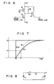
- the word lines W1 to WM are connected at both ends to positive feedback amplifiers PFAO-1 to PFAO-M and PFA1-1 to PFA1-M, respectively. These positive feedback amplifiers each have a construction as shown in Fig. 6.
- the positive feedback amplifier shown in Fig. 6 has a p-channel MOS FET 10 having a source connected to a positive power source terminal V D , an n-channel MOS FET 12 having a source connected to a reference power source terminal Vs and a drain connected to the drain of the p-channel MOS FET 10, and a p-channel MOS FET 14 having a gate connected to the drains of the FETs 10 and 12 and a source connected to the positive power source terminal V D .
- a resistor 16 is connected in parallel with a current path of the MOS FET 10.
- the gate of the MOS FET 10 is coupled with a clock pulse receiving terminal Vp for receiving a low level clock pulse for a given period of time each time the memory operating cycle changes.
- the gate of the MOS FET 12 and the drain of the MOS FET 14 are connected to the same word line.
- MOS FET 10 In response to clock pulses supplied to the clock receiving terminal Vp, MOS FET 10 is made conductive every memory cycle, that is, every time the address signal is changed, for a given period of time, thereby to precharge the drain of the MOS FET 12 to a high level. For example, when an access signal is applied to the word line and a potential on the word line exceeds the threshold voltage of the MOS FET 12, the MOS FET 12 conducts, so that the drain voltage of the MOS FET decreases toward a reference voltage. When the drain voltage of the MOS FET 12 reaches the threshold voltage of the MOS FET 14, the potential level of the word line is pulled up to a high level by way of the MOS FET 14.
- Fig. 7 illustrates a variation of a voltage level of an access signal with a voltage level V A on the word line when the access signal is produced on the word line at time To.
- a solid line SL1 shows a voltage variation of the access signal on the portion of the word line at the farthest distance from the decoder 2 when the positive feedback amplifier is not used.
- Another solid line SL2 illustrates a voltage variation of the access signal on the portion of the word line near the decoder 2.
- Fig. 8 shows an equivalent circuit of a word line segment ranging from the decoder 2 to the positive feedback amplifier.
- a battery E produces an output voltage V A
- a resistor R and a capacitor C express the resistance and the stray capacitance of the word line segment in the lamped constant manner.
- a switch SW in the circuit is closed at time To, a potential at a junction P between the resistor R and the capacitor C changes as indicated by the solid line SL1 in Fig. 7.
- a potential Vx of the access signal on the word line at time T, which is depicted by the line SL1 is mathematically given by the following equation:
- the positive feedback amplifier is coupled with the word line at a distance from the row decoder 2, whereby the voltage rise on the word line, due to the access signal, is made steep, and the access time to the memory cell located near the positive feedback amplifier is remarkably reduced.
- Fig. 9 shows a modification of the positive feedback amplifier circuit shown in Fig. 6.
- the circuit is the same as that shown in Fig. 6 except that it has additionally an n-channel MOS FET 18 which has a drain coupled with a word line connecting terminal Vw connected to the word line, a source connected to the reference power source terminal Vs, and a gate connected to the clock pulse receiving terminal V,p for receiving clock pulses which are opposite in phase to the pulses applied to the gate of the MOS FET 10.
- the potential on the word line selected changes from high level to low as the row address designation period terminates. At a distance from the decoder 2, the potential change on the word line is slow.
- the positive feedback amplifier circuit shown in Fig. 9 a high level signal is applied to the clock pulse receiving terminal V ⁇ as the low address designating period terminates, to render the MOS FET 18 conductive and to instantaneously reduce to the low level the potential at the word line connecting terminal Vw, that is, the potential on the portion of the word line coupled with the positive feedback amplifier.
- the use of the positive feedback amplifier circuit shown in Fig. 9 may quickly permit a potential change on the word line.
- Fig. 10 shows a modification of the positive feedback amplifier circuit shown in Fig. 9.
- the circuit in Fig. 10 is similar to that of Fig. 9 except that a p-channel MOS FET 20 is used in place of the resistor 16.
- the source of the MOS FET 20 is coupled with the power source terminal V D , the drain is connected to the gate of the MOS FET 14, and the gate is connected to the word line connecting terminal Vw.
- the pairs of the word lines are used for the memory-cells on each column.
- the paired data lines may be substituted by single data lines if the dynamic memory cells as shown in Fig. 11 are used.
- Fig. 12 shows a matrix memory array having memory cells DMC-11 to DMC-MN each with a similar construction to that of the memory cell shown in Fig. 11.
- the Fig. 12 embodiment also has the useful effect like the Fig. 3 embodiment.
- the positive feedback amplifier circuits which are connected to both ends of the word lines in Fig. 3, may be connected to the word lines at the portion thereof far from the row decoder 2.
- the decoder 2 which is disposed at the substantially central portion of the memory array in the embodiment shown in Fig. 3, may be disposed at other suitable location. In an extreme example, it may be connected to one end of the word lines, as shown in Fig. 1. In this case, the positive feedback circuit is connected to the other side of the word lines or near the same.
Landscapes
- Engineering & Computer Science (AREA)
- Microelectronics & Electronic Packaging (AREA)
- Computer Hardware Design (AREA)
- Dram (AREA)
- Static Random-Access Memory (AREA)
Claims (10)
Applications Claiming Priority (2)
| Application Number | Priority Date | Filing Date | Title |
|---|---|---|---|
| JP95526/79 | 1979-07-26 | ||
| JP9552679A JPS5619585A (en) | 1979-07-26 | 1979-07-26 | Semiconductor memory unit |
Publications (3)
| Publication Number | Publication Date |
|---|---|
| EP0023655A2 EP0023655A2 (de) | 1981-02-11 |
| EP0023655A3 EP0023655A3 (en) | 1982-11-17 |
| EP0023655B1 true EP0023655B1 (de) | 1985-07-03 |
Family
ID=14139989
Family Applications (1)
| Application Number | Title | Priority Date | Filing Date |
|---|---|---|---|
| EP80104250A Expired EP0023655B1 (de) | 1979-07-26 | 1980-07-18 | Halbleiter-Speichervorrichtung |
Country Status (4)
| Country | Link |
|---|---|
| US (2) | US4379346A (de) |
| EP (1) | EP0023655B1 (de) |
| JP (1) | JPS5619585A (de) |
| DE (1) | DE3070830D1 (de) |
Families Citing this family (16)
| Publication number | Priority date | Publication date | Assignee | Title |
|---|---|---|---|---|
| JPS5819794A (ja) * | 1981-07-29 | 1983-02-04 | Fujitsu Ltd | 半導体メモリ |
| JPS58169958A (ja) * | 1982-03-31 | 1983-10-06 | Fujitsu Ltd | Misスタテイツク・ランダムアクセスメモリ |
| JPS61178795A (ja) * | 1985-02-01 | 1986-08-11 | Toshiba Corp | ダイナミツク型半導体記憶装置 |
| JPS62149097A (ja) * | 1986-12-12 | 1987-07-03 | Mitsubishi Electric Corp | 半導体メモリ装置 |
| USRE37055E1 (en) | 1989-08-18 | 2001-02-20 | Michael A. Silveri | Pool purifier attaching apparatus and method |
| US5580438A (en) * | 1989-08-18 | 1996-12-03 | Silveri; Michael A. | Pool purifier attaching apparatus and method |
| US5759384A (en) | 1995-03-30 | 1998-06-02 | Bioquest | Spa halogen generator and method of operating |
| US6007693A (en) | 1995-03-30 | 1999-12-28 | Bioquest | Spa halogen generator and method of operating |
| US5545310A (en) | 1995-03-30 | 1996-08-13 | Silveri; Michael A. | Method of inhibiting scale formation in spa halogen generator |
| US5676805A (en) | 1995-03-30 | 1997-10-14 | Bioquest | SPA purification system |
| US5752282A (en) | 1995-03-30 | 1998-05-19 | Bioquest | Spa fitting |
| US6252843B1 (en) | 1999-04-09 | 2001-06-26 | Hewlett Packard Company | Automatic clamping of compact discs |
| DE10050770A1 (de) * | 2000-10-13 | 2002-05-02 | Infineon Technologies Ag | Schaltungsanordnung zum Steuern der Wortleitungen einer Speichermatrix |
| US9105315B2 (en) | 2012-07-23 | 2015-08-11 | Arm Limited | Controlling the voltage level on the word line to maintain performance and reduce access disturbs |
| GB2520277B (en) * | 2013-11-13 | 2016-07-20 | Advanced Risc Mach Ltd | Controlling the voltage level on the word line to maintain performance and reduce access disturbs |
| JP7242285B2 (ja) * | 2018-12-19 | 2023-03-20 | キオクシア株式会社 | 半導体装置 |
Family Cites Families (16)
| Publication number | Priority date | Publication date | Assignee | Title |
|---|---|---|---|---|
| US955006A (en) * | 1909-01-27 | 1910-04-12 | Joseph Everett Sparks | Abdominal retractor. |
| US3644905A (en) * | 1969-11-12 | 1972-02-22 | Gen Instrument Corp | Single device storage cell for read-write memory utilizing complementary field-effect transistors |
| US3657568A (en) * | 1970-01-05 | 1972-04-18 | Hamilton Watch Co | Pulse shaping circuit using complementary mos devices |
| US3810124A (en) * | 1972-06-30 | 1974-05-07 | Ibm | Memory accessing system |
| US3989955A (en) * | 1972-09-30 | 1976-11-02 | Tokyo Shibaura Electric Co., Ltd. | Logic circuit arrangements using insulated-gate field effect transistors |
| US3845328A (en) * | 1972-10-09 | 1974-10-29 | Rca Corp | Tri-state logic circuit |
| JPS5178665A (de) * | 1974-12-24 | 1976-07-08 | Ibm | |
| US4069475A (en) * | 1976-04-15 | 1978-01-17 | National Semiconductor Corporation | MOS Dynamic random access memory having an improved sense and restore circuit |
| US4080539A (en) * | 1976-11-10 | 1978-03-21 | Rca Corporation | Level shift circuit |
| US4071783A (en) * | 1976-11-29 | 1978-01-31 | International Business Machines Corporation | Enhancement/depletion mode field effect transistor driver |
| JPS53140962A (en) * | 1977-05-16 | 1978-12-08 | Hitachi Denshi Ltd | Electronic switch circuit |
| US4168536A (en) * | 1977-06-30 | 1979-09-18 | International Business Machines Corporation | Capacitor memory with an amplified cell signal |
| JPS54152845A (en) * | 1978-05-24 | 1979-12-01 | Hitachi Ltd | High dielectric strength mosfet circuit |
| JPS5567235A (en) * | 1978-11-14 | 1980-05-21 | Nec Corp | Output circuit |
| JPS55150189A (en) * | 1979-05-10 | 1980-11-21 | Nec Corp | Memory circuit |
| JPS5625291A (en) * | 1979-08-07 | 1981-03-11 | Nec Corp | Semiconductor circuit |
-
1979
- 1979-07-26 JP JP9552679A patent/JPS5619585A/ja active Pending
-
1980
- 1980-07-18 EP EP80104250A patent/EP0023655B1/de not_active Expired
- 1980-07-18 DE DE8080104250T patent/DE3070830D1/de not_active Expired
- 1980-07-21 US US06/170,687 patent/US4379346A/en not_active Expired - Lifetime
-
1984
- 1984-11-08 US US06/669,724 patent/US4535255A/en not_active Expired - Lifetime
Non-Patent Citations (1)
| Title |
|---|
| IEEE INTERNATIONAL SOLID-STATE CIRCUITS CONFERENCE, vol. 16, no. 73, 14th February 1973, pages 64-65, New York, USA W.K. HOFFMAN et al: "An 8-k Bit random-access memory chip using a one-device FET cell". * |
Also Published As
| Publication number | Publication date |
|---|---|
| EP0023655A3 (en) | 1982-11-17 |
| US4379346A (en) | 1983-04-05 |
| JPS5619585A (en) | 1981-02-24 |
| EP0023655A2 (de) | 1981-02-11 |
| US4535255A (en) | 1985-08-13 |
| DE3070830D1 (en) | 1985-08-08 |
Similar Documents
| Publication | Publication Date | Title |
|---|---|---|
| JP2611504B2 (ja) | 半導体メモリ | |
| KR930001554B1 (ko) | 다이나믹 반도체 기억장치와 그 구동방법 | |
| US4616342A (en) | Semiconductor memory device | |
| US4421996A (en) | Sense amplification scheme for random access memory | |
| EP0023655A2 (de) | Halbleiter-Speichervorrichtung | |
| EP0023329A2 (de) | Halbleiter-Speichervorrichtung | |
| KR100208062B1 (ko) | 반도체기억장치 | |
| EP0264929B1 (de) | Halbleiterspeicheranordnung mit verbesserter Bitzeilenordnung | |
| KR930006725A (ko) | 반도체 기억장치 | |
| EP0175880A2 (de) | Halbleiterspeicheranordnung | |
| US5058072A (en) | Semiconductor memory device with high speed sensing facility | |
| EP0185451B1 (de) | Halbleiterspeicheranordnung mit Leseverstärkern | |
| US5870343A (en) | DRAM sensing scheme for eliminating bit-line coupling noise | |
| JPH0373080B2 (de) | ||
| EP0846326A1 (de) | Ladungsübertragungsabtastverstärker | |
| US6016279A (en) | DRAM sensing scheme and isolation circuit | |
| KR960009946B1 (ko) | 반도체 메모리 디바이스 | |
| US4045785A (en) | Sense amplifier for static memory device | |
| US5406512A (en) | Semiconductor memory device using compensation capacitors | |
| US3629612A (en) | Operation of field-effect transistor circuit having substantial distributed capacitance | |
| EP0036932B1 (de) | Leseverstärkersystem und Speicher | |
| US5982692A (en) | Bit line boost amplifier | |
| JP2980368B2 (ja) | ダイナミック型半導体記憶装置 | |
| JPH0758592B2 (ja) | 半導体メモリ | |
| US4875194A (en) | Semiconductor memory device with protection cells |
Legal Events
| Date | Code | Title | Description |
|---|---|---|---|
| PUAI | Public reference made under article 153(3) epc to a published international application that has entered the european phase |
Free format text: ORIGINAL CODE: 0009012 |
|
| 17P | Request for examination filed |
Effective date: 19800718 |
|
| AK | Designated contracting states |
Designated state(s): DE FR GB |
|
| PUAL | Search report despatched |
Free format text: ORIGINAL CODE: 0009013 |
|
| AK | Designated contracting states |
Designated state(s): DE FR GB |
|
| RAP1 | Party data changed (applicant data changed or rights of an application transferred) |
Owner name: KABUSHIKI KAISHA TOSHIBA |
|
| GRAA | (expected) grant |
Free format text: ORIGINAL CODE: 0009210 |
|
| AK | Designated contracting states |
Designated state(s): DE FR GB |
|
| REF | Corresponds to: |
Ref document number: 3070830 Country of ref document: DE Date of ref document: 19850808 |
|
| ET | Fr: translation filed | ||
| PLBE | No opposition filed within time limit |
Free format text: ORIGINAL CODE: 0009261 |
|
| STAA | Information on the status of an ep patent application or granted ep patent |
Free format text: STATUS: NO OPPOSITION FILED WITHIN TIME LIMIT |
|
| 26N | No opposition filed | ||
| REG | Reference to a national code |
Ref country code: GB Ref legal event code: 746 Effective date: 19990216 |
|
| PGFP | Annual fee paid to national office [announced via postgrant information from national office to epo] |
Ref country code: FR Payment date: 19990709 Year of fee payment: 20 |
|
| PGFP | Annual fee paid to national office [announced via postgrant information from national office to epo] |
Ref country code: GB Payment date: 19990714 Year of fee payment: 20 |
|
| PGFP | Annual fee paid to national office [announced via postgrant information from national office to epo] |
Ref country code: DE Payment date: 19990716 Year of fee payment: 20 |
|
| REG | Reference to a national code |
Ref country code: FR Ref legal event code: D6 |
|
| PG25 | Lapsed in a contracting state [announced via postgrant information from national office to epo] |
Ref country code: GB Free format text: LAPSE BECAUSE OF EXPIRATION OF PROTECTION Effective date: 20000717 |
|
| REG | Reference to a national code |
Ref country code: GB Ref legal event code: PE20 Effective date: 20000717 |