EP0024663A2 - Système de traitement d'information, avec une structure de barre omnibus modulaire et une configuration expansible - Google Patents
Système de traitement d'information, avec une structure de barre omnibus modulaire et une configuration expansible Download PDFInfo
- Publication number
- EP0024663A2 EP0024663A2 EP80104872A EP80104872A EP0024663A2 EP 0024663 A2 EP0024663 A2 EP 0024663A2 EP 80104872 A EP80104872 A EP 80104872A EP 80104872 A EP80104872 A EP 80104872A EP 0024663 A2 EP0024663 A2 EP 0024663A2
- Authority
- EP
- European Patent Office
- Prior art keywords
- peripheral
- input
- output
- signal
- peripherals
- Prior art date
- Legal status (The legal status is an assumption and is not a legal conclusion. Google has not performed a legal analysis and makes no representation as to the accuracy of the status listed.)
- Granted
Links
Images


Classifications
-
- G—PHYSICS
- G06—COMPUTING OR CALCULATING; COUNTING
- G06F—ELECTRIC DIGITAL DATA PROCESSING
- G06F13/00—Interconnection of, or transfer of information or other signals between, memories, input/output devices or central processing units
- G06F13/14—Handling requests for interconnection or transfer
- G06F13/20—Handling requests for interconnection or transfer for access to input/output bus
- G06F13/24—Handling requests for interconnection or transfer for access to input/output bus using interrupt
- G06F13/26—Handling requests for interconnection or transfer for access to input/output bus using interrupt with priority control
Definitions
- the present invention relates to the architecture of data processing systems which make use of microprocessors intercommunicating oy means of a common system channel or 3US. More particularly it relates to the circuits and the priority mechanism, through which the conflicts in the common use of the BUS among the several microprocessors of the system are solved.
- LSI large scale integration
- Such components perform by themselves the most of the required logical and circuital functions, and allow to obtain the desired system product with the addition of few electrical and/or functional components.
- Such integrated components widely perform, as the case may be, the function of central units or the one of interface control units for connection of peripheral devices.
- Such family includes, for example, a microprocessor, with identification code Z-80 CPU, which performs the specific function of central and control unit in a data processing system and a microprocessor,with identification code Z-80 PIO, which performs the interface functions of two parallel interface input/output channels, in order to connect to the system peripheral devices such as punching machines, printers, keyboards and so on.
- Another exemplary microprocessor of the family performs the function of interface having serial input/ output channel in order to connect to the system transmission lines and peripheral devices with serial interface such as disk units, tape cassette units and so on.
- a simple system built up with such family components may include, for example, a Z-80 CPU with function of central unit, an oscillator for the generation of timing signals, a power supply for the generation of a +5V regulated voltage supply, a read only memory for containing the microprograms required to lead the operation of the system and a peripheral Z-80 PIO (or SIO) coupled to an input/output peripheral unit such as a keyboard/printer set.
- a Z-80 CPU with function of central unit
- an oscillator for the generation of timing signals
- a power supply for the generation of a +5V regulated voltage supply
- a read only memory for containing the microprograms required to lead the operation of the system
- a peripheral Z-80 PIO or SIO
- More complex systems may include, in addition to the read only memory, one or more read/write working memories for data and programs storing, and a plurality of peripherals such as Z-80 PIO (or SIO), each one connected to the common system bus.
- peripherals such as Z-80 PIO (or SIO), each one connected to the common system bus.
- This kind of architecture makes possible the assembling of flexible systems, based on modular elements which can be added or removed according to the needs to obtain the most suitable configurations for the required functions.
- a system can be materially built up as a chassis or rack where a number N of printed circuit boards can be housed.
- the rack rear is provided with a plurality N of connector sockets for printed circuit boards.
- corrisponding contact elements of each connector socket are all connected together by electrical connection lines, obtained by means of the "wire wrap” technology or preferably by means of conductive leads formed on printed circuit board.
- This board is usually named "back panel”.
- a printed circuit board can include the microprocessor Z-80 CPU, the oscillator and other possible circuits, suitable for the microprocessor operation.
- a second board can include a control RCS memory.
- One or several additional board can include a read/write working memo ry and further boards can include one or several interface peripherals each.
- each peripheral can send an interrupt request signal to the CPU central unit through a lead specifically assigned to each peripheral.
- the plurality of such leads is connected to the input of a network which detects interruptions and selects one of them on a priority basis.
- the selection operation too generally requires a group of leads, each one of which is "dedicated" to a peripheral, that is it connects the selection network to a peripheral.
- each peripheral is furnished with an internal masking mechanism which allows to inhibit or mask the interruption request generation from each peripheral if such peripheral defects the presence of more prioritary interruptions.
- the priority of each peripheral is determined by its position in an inhibition chain.
- Each peripheral has an interruption enabling input (IEI) and an inter ruption enabling output (IEO).
- IIEI interruption enabling input
- IEO inter ruption enabling output
- the identification of the interrupting peripheral occurs through the sending on the BUS lead of an "interrupt vector" which supplies directly or indirectly the identity of the interrupting peripheral.
- the selection of the interrupting peripheral too can be made through the sending on the BUS leads of an address vector identified through a decoder by the interested peripheral only.
- the interruption masking mechanism requires the transfer of a signal in the chain of peripherals with a propagation time from peripheral to peripheral in the order of 200 nsec and stric tly limits the number of peripherals which can be effectively connected to the BUS.
- Such network which is identical on each printed circuit plate,provides an intrinsically very fast by pass path for the interruption masking signal around each peripheral and, within the system, provides a matrix connection network instead of a cascade connection.
- microprocessor system object of present invention allows for the assembly of several peripherals on the same plate, still maintaining a good flexibility in the assignment of the relative prio rities among the several peripherals.
- Figure 1 represents, in block diagram, a system architecture known in the art, which uses a chain interrupting mechanism.
- the system includes a central unit, or CPU 1, a microprogram memory or ROS 2 and a certain number of peripherals 3, 4, 5, 6, each one connected to the one or to a group of peripheral units 7, 3, 9, 1 0 .
- Such channel is formed by a certain number of leads for the transfer of data, commands, signals, addresses.
- the access to the BUS is managed and controlled by the CPU1, which can issue commands or authorization signals to the several peripherals, memory included, to use the BUS leads and to apply thereon electrical signals representative of information.
- the peripherals can ask, through an interruption, to access the BUS 11 on their own initiative as a consequence of the rising of particular events or status inside them or inside the peripheral units to which they are connected.
- All the peripherals are provided with an output, respectively INT 3, INT 4, INT 5, connected to a common lead 12, which in turn is connected to an input INT 1 of CPU 1 and is normally maintained at a positi ve electrical level by a pull up resistor 13, connected to a +V volta ge source.
- Such electrical level variation is detected by the CPU at suitable times through input INT 1 and, after a certain time interval, the CPU sends on BUS 11 (or better on some BUS leads) some answer signals with the meaning of interruption acceptance.
- each peripheral is provided with an internal interruption logic, with an input terminal IEI3, IE14, IEI5, IEI6 respecti vely and with an output terminal IE03, IEO4, IE05, IEO6, respectively.
- Each peripheral can effectively forward an interruption (that is to lower to 0 the level of lead 12) only if a positive electrical signal (or logical level 1) is present on its input IEI.
- each peripheral normally keeps its output IEO at positi ve electrical level (or logical level 1) and lowers it to electrical/ logical level 0 when it produces an interruption or when its input IEI is lowered to 0.
- each peripheral is able to identify an interruption accepting signal only if it has sent an interruption and this is not masked.
- the input IEI3 of the first'peripheral of the chain will permanently be held at a positive level, for instance by means of a connection with a voltage source +V through a resistor 14.
- the CPU has to wait some time before taking into ac- co-nt a pending interruption in order to be sure that such interruption is due to one and only one peripheral at each time and that its answer (interruption acceptance) is recognized by the interrupting peripheral only.
- the interrupting peripheral When the interrupting peripheral, it and it only, recognizes that an interruption acceptance answer has been sent to it, it puts on the BUS leads an information which specifies, for example, its name or the initial address of an interrupt handling program, or other information used by CPU to get suitable measures.
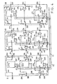
- FIG. 2 shows a preferred embodiment of the invention with reference to a system comprising 9 interrupting peripherals, respectively numbe red from 30 to 35.
- Each peripheral is mounted on a printed circuit board (being the boards numbered from 40 to 48) and each board can in clude auxiliary circuits, not shown, and interface circuits for coupling with peripheral devices or transmission lines.
- Each plate is supplied with a connection edge or a plug for insertion in an interconnection socket mounted on the "back panel" of a rack.
- the connection edge of each board includes a suitable number of input and output pins, which in figure 2 are shown, for clearness sake, as located on different sides of each board.
- connection edge has:
- references of the several pins are formed by ad ding a cipher to the plate reference number.
- each plate is provided with a network for speeding up the masking operation.
- the network includes two AND gates 406, 407, each one with two inputs.
- the first AND gate 4C6 has its output connected to the input IEI of peripheral 30 and its two inputs respectively connected to pins 401, 402 of the board.
- the two inputs are normally held at a voltage level +V through two re sistors 408, 409 of suitable value, connected between such inputs and a voltage source +V.
- the second AND gate 407 of the "open collector” type, has its output connected to pin 403, a first input directly connected to the ITOout put of peripheral 30 and the second input connected, through lead 400, to the output of AND gate 406.
- Pin 404 is connected to BuS lead 12, used for the transfer of the interruption signal (INT).
- Pins 405 are connected to the remaining BUS leads 11.
- pins 414, 424 ?? 484 of the several boards are all connec ted to BUS lead 12 and pins 415, 425 ?? 485 of the several plates are all connected to the other BuS leads.
- Such leads or connection elements are formed on the "back panel”.
- peripherals 30, 31, .... 38 and the corresponding boards 40, 41, .... 48, to which an interrupting power with decreasing priority from peripheral 30 to peripheral 38 is ascribed are logically organi zed in a matrix of 3 lines and 3 columns.
- the matrix of fig. 2 includes a first line formed, in the order, by boards 40, 41, 42, a second line formed in the order by boards 45, 44, 43 and a third line formed by boards 46, 47, 48.
- the output pin 403 of board 40 is connected through connection 301 to pin 412 of board 41. It is further connected, through connection 302, to pin 451 od board 45.
- the output pin 413 of board 41 is connected, through connection 303, to pin 422 of board 42. It is further connected, through connection 304, to pin 441 of board 44.
- the output pin 423 of board 42 is connected, through connection 305, to pin 431 of board 43.
- the output pin 433 of board 43 is connected, through connection 306, to pin 442 of board 44. It is further connected, through connection 307, to pin 481 of board 48.
- the output pin 443 of board 44 is connecteted through connection 306 to pin 452 of board 45. It is further connected, through connection 309, to pin 47 1 of board 47.
- the output pin 453 of board 45 is connected through connection 310 to pin 461 of board 46.
- the output pin 463 of board 46 is connected through connection 311 to pin 472 of board 47.
- the output pin 473 of board 47 is connected to pin 482 of board 48 through connection 312.
- MxN peripherals each one mounted on a board
- N lines and N columns may be considered.
- the board Pij output pin which is used to transfer the interrupt enable/inhibit signal, is indicated by (this is the pin corresponding to pins 403, 413, 423, .... 483 of fig. 2); if the two input pins of board Pij, which receive the interrupt enable/inhibit signal, are indicated by I1ij and I2ij, then the interconnection among the boards connects the output pin Uij with the input pins I1i+1,j and I2i,j+1 with the following conditions:
- an interrupt/inhibition signal at logic level 0 possibly applied to input 401, 402, spreads to input IEIof peripheral 30 with a propa gation time determined by AND gate 406.
- Such time is of about ten nsec, in case the TTL technology, generally adopted for the realization of such circuits, is used.
- connection 400 From here the signal spreads, through connection 400 and AND gate 407, to output 403 with a further delay of about 10 nsec.
- the total propagation delay of a signal at logic level C from inputs 401, 402 to out put 403 is therefore of 20 nsec.
- connections between the several boards form a system of peripherals with decreasing priority from 30 to 38, that is a system of boards with decreasing priority from 40 to 48.
- peripheral 30 if peripheral 30 generates an interruption signal, it lowers at the same time its output I ⁇ O at logic level 0 and such level spreads to pin 403 and then, through pin 412 and AND gate 416, to peripheral 31, inhibiting or masking in such last one the possible interrupt requests.
- peripheral 30 generates an inhibit signal to IEO output, such signal is transferred, in addition to peripheral 31 of the same line, to peripheral 35 of the same column, through connections 302 as well as, through the speed up network of board 45, to peripheral 36 of the same column too.
- inhibit/interrupt signal spreads through peripherals in cascade, not only according to a line order, but according to a column order too and this is obviously valid for all the peripherals of the system.
- the propagation time reduction becomes still more relevant in systems of more lines and colums.
- the propagation time is therefore reduced almost to a third.
- the boards have identical speed up networks because it allows their complete position interchangeability within the matrix.
- FIG. 2 A second important remark is that in figure 2 a central unit CPU 1, which controls the system of peripherals, is shown as an element which is not inoluded in the peripheral matrix.
- the network function is only to establish a connection between two input pins of the plate and an output pin with obvious simplification.
- a third important remark is that a system of peripherals need not to be complete, in the sense that, once provided a mechanical architectu re and a "back panel" circuit arranged to fit with a MxN board number. it is not required that the system actually includes MxN boards; on the contrary it can include a lower number of them.
- Figure 3 shows, in perspective, the mechanical architecture according to which the system of figure 2 is preferably embodied.
- a printed circuit plate which, according to the needs, may be single, double or multilayer provides a back panel 500.
- connection sockets 59, 60, .... 68 are mounted on board 500, for instance by welding, in parallel stacked fashion, each one being intended to receive the edge of a printed circuit board where the connection pins are located.
- Board 100 containing CPU 1, is inserted into socket 59, board 40 into socket 60, board 41 into socket 61 and so on up to board 48 which is inserted into socket 68.
- the socket conducting elements (not in sight) are welded to as many back panel pads and establish an electrical connection between the pins of the boards 100, 40, .... 48 and the pads.
- Back panel 500 bears in sight the several printed leads which form BUS 11, the interrupt lead 12, and the prioritary network leads alrea dy numbered from 301 to 312 in figure 2.
- BUS 11 and lead 12 extend to socket 59 and set an electrical connection with the CPU board 100.
- the only requirement for functionality of the prioritary network is the ordered arrangement of the system boards in the first interconnection sockets, from socket 59.
- the priority awarding and the interrupt masking matrix system which is the object of the present invention, can be used in EDP systems where a plurality of peripherals is mounted on a single board.
- some interconnection leads, indicated in figures2 and 3 as formed on the "back panel" can be directly made on the peripheral boards.
- FIG. 4 shows such embodiment.
- Board I includes a central unit CPU 227, a memory unit MM 228 and a peripheral 229.
- Board II includes three peripherals 230, 231, 232 and board III inclu des two peripherals 233, 234.
- the boards can include a variable number of peripherals, as well as logic units other than periphérals, which do not intervene in the interruption generation and masking process, such as the central unit and the memory. To allow for the most complete position interchangeability among the boards, they are provided with the same number of input and output pins, identically located.
- each plate has a pin, respectively 235, 236, 237 for connection to BUS lead 12, dedicated to the transfer of the interrupt signal, a pin set, respectively 238, 239, 240,for the interconnection of the se veral peripherals and of the memory units or CPU with BUS leads 11, and a plurality of input pins,respectively 201, 204, 205 for plate I, 211, 214, 215 for plate II, 221, 224, 225 for plate III, intended to receive input IEI enable/inhibit signals, as well as a plurality of output pins,respectively 202, 203, 206 for plate I,. 212, 213, 216 for plate II and 222, 223, 226 for plate III,intended to transfer output IEO enable/inhibit signals.
- Such input and output pins for the transfer of signals IEI, IEO are suitably connected among themselves in order to form a matrix network for interruption transfer and masking.
- Pins 201 and 202 are related to CPU 227 but, since CPU does not inter vene in the interruption generation and masking mechanism, such pins are not interconnected with the CPU and are directly connected together through lead 241.
- Pins203 and 204 are related to memory 228 but, since the memory does not operate in the interruption generation and masking mechanism, such pins are not interconnected with memory and are connected together by lead 243 and through the two input AND gate 244 of the "open collector" type.
- An input of AND gate 244 is connected to pin 204; the second input is connected t6 pin 202 through lead 245.
- Pins 203 and 204 are normally held at positive level through "pull up" resistors 246 and 207 respectively.
- Pins 205 and 206 are coupled to peripheral 229.
- Pin 205 is connected to an input of a two inputs AND gate 247 and it is normally held at positive level by a "pull up" resistor 208.
- the second input of AND gate 247 is connected to pin 203 through lead 248.
- AND gate 247 is connected to input IEI of peripheral 229. It is further connected to an input of a two input AND gate 250, of the open collector type, through a "by pass" lead 249.
- the second input of gate 250 is connected to output IEO of peripheral 229.
- the output of AND gate 250 is connected to pin 206.
- pins 211. and 212 are coupled to peripheral 230.
- Pin 211 is connected to input IEI of peripheral 230 and, through a "by pass” lead 252 to an input of a two input AND gate 253, of the "open collector” type.
- the second input of AND gate 253 is connected to output IEO of periphe ral 230.
- the output of AND gate 253 is connected to pin 212 and is normally held at positive level by "pull up" resistor 217.
- Pin 213 and 214 are coupled to peripheral 231.
- Pin 214 is connected to an input of a two inputs AND gate 254 and it is normally held at positive level by pull-up resistor 219.
- the second input of AND 254 is connected to output of AND gate 253 through lead 213.
- AND gate 254 is connected to input IEI of peripheral 231 and through lead 255 to an input of a two input AND gate 250 of the "open collector" type.
- the output is connected to pin 213 and it is normally held at positive level by a pull-up resistor 257.
- Pins 215 and 216 are coupled to peripheral 232.
- Pin 215 is connected to an input of a two input AND gate 253 and it is normally held at positive level by the "pull-up" resistor 259.
- the second input of AND gate 258 is connected to pin 213 through lead 260.
- the AND gate 258 output is connected to IEI input of peripheral 232 and through lead 261 to an input of a two input open collector AND gate 262.
- the second input of AND gate 262 is connected to output IEO of peripheral 232 and its output is connected to pin 216.
- pins 221 and 222 are coupled to peripheral 233.
- Pin 221 is connected to input IEI of peripheral 233 and, through lead 263, to an input of a two input "open collector” AND gate 264.
- the second input of AND gate 264 is connected to output IEO of peripheral 233 and its output is connected to tap 222 and normally held at positive level by "pull up" resistor 266.
- Pins 223 and 224 are not coupled to any peripheral and are located on the board only to assure the identity among the several board as concerns the input and output terminals and therefore their position interchangeability within the system architecture.
- Pins 223 and 224 are interconnected each other by circuits which complete the network architecture of the circuits and of the interrupt and masking mechanism.
- Pin 224 is connected to an input of a two input "open collector” AND gate 267.
- the second input of AND gate 267 is connected to pin 222 through lead 269.
- the AND gate 267 output is connected to pin 223 and it is normally held at positive level by the "pull-up" resistor 270.
- Pins 225 and 226 are coupled to peripheral 234.
- Pin 225 is connected to an input of a two input AND gate 228 and it is normally held at positive level by "pull up resistor 271.
- the second input of AND gate 228 is connected to pin 223 through lead 227.
- the AND gate 228 output is connected to input IEI of peripheral 234 and, through lead 272, to an input of a two input "open collector” AND gate 229.
- AND gate 229 is connected to output IEO of peripheral 234 and its output is connected to pin 226.
- the several boards are interconnected each other through the leads of a back panel. Particularly the couples of pins 202 and 211, 204 and 213, 206 and 215, 212 and 221, 214 and 213, 216 and 225 are connected each other.
- the system architecture can be extended indefinitely by connecting pins 222, 224, 226 to corresponding pins of a fourth board and so on.
- Figure 5 shows the "back panel" 273 of a system formed with boards li ke the ones of figure 4.
Landscapes
- Engineering & Computer Science (AREA)
- Theoretical Computer Science (AREA)
- Physics & Mathematics (AREA)
- General Engineering & Computer Science (AREA)
- General Physics & Mathematics (AREA)
- Bus Control (AREA)
- Multi Processors (AREA)
Applications Claiming Priority (2)
| Application Number | Priority Date | Filing Date | Title |
|---|---|---|---|
| IT25356/79A IT1122890B (it) | 1979-08-30 | 1979-08-30 | Sistema a microprocessori con struttura modulare a bus e configurazione espandibile |
| IT2535679 | 1979-08-30 |
Publications (3)
| Publication Number | Publication Date |
|---|---|
| EP0024663A2 true EP0024663A2 (fr) | 1981-03-11 |
| EP0024663A3 EP0024663A3 (en) | 1981-09-09 |
| EP0024663B1 EP0024663B1 (fr) | 1985-04-17 |
Family
ID=11216458
Family Applications (1)
| Application Number | Title | Priority Date | Filing Date |
|---|---|---|---|
| EP80104872A Expired EP0024663B1 (fr) | 1979-08-30 | 1980-08-16 | Système de traitement d'information, avec une structure de barre omnibus modulaire et une configuration expansible |
Country Status (5)
| Country | Link |
|---|---|
| US (1) | US4417302A (fr) |
| EP (1) | EP0024663B1 (fr) |
| JP (1) | JPS5642831A (fr) |
| DE (1) | DE3070510D1 (fr) |
| IT (1) | IT1122890B (fr) |
Cited By (1)
| Publication number | Priority date | Publication date | Assignee | Title |
|---|---|---|---|---|
| EP0113401A1 (fr) * | 1982-11-04 | 1984-07-18 | HONEYWELL INFORMATION SYSTEMS ITALIA S.p.A. | Appareil de connexion en étoile au moyen d'un câble plat |
Families Citing this family (24)
| Publication number | Priority date | Publication date | Assignee | Title |
|---|---|---|---|---|
| FR2494010B1 (fr) * | 1980-11-07 | 1986-09-19 | Thomson Csf Mat Tel | Dispositif d'arbitration decentralisee de plusieurs unites de traitement d'un systeme multiprocesseur |
| USRE33705E (en) * | 1982-02-24 | 1991-10-01 | Digital Equipment Corporation | Interchangeable interface circuit structure |
| JPS5924327A (ja) * | 1982-07-30 | 1984-02-08 | Hitachi Ltd | 分散形優先選択装置 |
| US4769768A (en) * | 1983-09-22 | 1988-09-06 | Digital Equipment Corporation | Method and apparatus for requesting service of interrupts by selected number of processors |
| US5067071A (en) * | 1985-02-27 | 1991-11-19 | Encore Computer Corporation | Multiprocessor computer system employing a plurality of tightly coupled processors with interrupt vector bus |
| US4858173A (en) * | 1986-01-29 | 1989-08-15 | Digital Equipment Corporation | Apparatus and method for responding to an aborted signal exchange between subsystems in a data processing system |
| US4839800A (en) * | 1986-08-29 | 1989-06-13 | Bull Hn Information Systems Inc. | Data processing system with a fast interrupt |
| JPS63100559A (ja) * | 1986-10-16 | 1988-05-02 | Sharp Corp | バス調停回路 |
| US5168568A (en) * | 1989-02-06 | 1992-12-01 | Compaq Computer Corporation | Delaying arbitration of bus access in digital computers |
| US5095460A (en) * | 1989-04-25 | 1992-03-10 | Digital Equipment Corporation | Rotating priority encoder operating by selectively masking input signals to a fixed priority encoder |
| US5247685A (en) * | 1989-11-03 | 1993-09-21 | Compaq Computer Corp. | Interrupt handling in an asymmetric multiprocessor computer system |
| JPH0814286B2 (ja) * | 1990-08-11 | 1996-02-14 | ティアツク株式会社 | スピンドル軸の軸受構造 |
| US5805841A (en) * | 1991-07-24 | 1998-09-08 | Micron Electronics, Inc. | Symmetric parallel multi-processing bus architeture |
| US5535395A (en) * | 1992-10-02 | 1996-07-09 | Compaq Computer Corporation | Prioritization of microprocessors in multiprocessor computer systems |
| US5553248A (en) * | 1992-10-02 | 1996-09-03 | Compaq Computer Corporation | System for awarding the highest priority to a microprocessor releasing a system bus after aborting a locked cycle upon detecting a locked retry signal |
| US5553310A (en) * | 1992-10-02 | 1996-09-03 | Compaq Computer Corporation | Split transactions and pipelined arbitration of microprocessors in multiprocessing computer systems |
| JPH08278916A (ja) * | 1994-11-30 | 1996-10-22 | Hitachi Ltd | マルチチャネルメモリシステム、転送情報同期化方法及び信号転送回路 |
| US5911055A (en) * | 1996-06-05 | 1999-06-08 | Compaq Computer Corporation | Using subordinate bus devices that are connected to a common bus |
| US5841969A (en) * | 1996-08-13 | 1998-11-24 | Honeywell Inc. | Single bus architecture supporting subsystems of various criticality levels |
| EP0913941B1 (fr) * | 1997-10-29 | 2003-09-17 | STMicroelectronics S.r.l. | Système de connexion de dispositif périphériques avec arbitrage de priorité, en particulier dans un émulateur de microcontrôleur à puce |
| US6314480B1 (en) * | 1998-11-09 | 2001-11-06 | Cirrus Logic, Inc. | Mixed-signal single-chip integrated system electronics for magnetic hard disk drives |
| US6618780B1 (en) * | 1999-12-23 | 2003-09-09 | Cirrus Logic, Inc. | Method and apparatus for controlling interrupt priority resolution |
| KR100528476B1 (ko) * | 2003-07-22 | 2005-11-15 | 삼성전자주식회사 | 컴퓨터 시스템의 인터럽트 처리 장치 |
| TW200810523A (en) * | 2005-12-23 | 2008-02-16 | Nxp Bv | An AV renderer peripheral with dual interrupt lines for staggered interrupts |
Family Cites Families (5)
| Publication number | Priority date | Publication date | Assignee | Title |
|---|---|---|---|---|
| US3800287A (en) * | 1972-06-27 | 1974-03-26 | Honeywell Inf Systems | Data processing system having automatic interrupt identification technique |
| US3832692A (en) * | 1972-06-27 | 1974-08-27 | Honeywell Inf Systems | Priority network for devices coupled by a multi-line bus |
| US3866181A (en) * | 1972-12-26 | 1975-02-11 | Honeywell Inf Systems | Interrupt sequencing control apparatus |
| US4123794A (en) * | 1974-02-15 | 1978-10-31 | Tokyo Shibaura Electric Co., Limited | Multi-computer system |
| JPS5259534A (en) * | 1975-11-11 | 1977-05-17 | Panafacom Ltd | Data transfer system |
-
1979
- 1979-08-30 IT IT25356/79A patent/IT1122890B/it active
-
1980
- 1980-08-16 DE DE8080104872T patent/DE3070510D1/de not_active Expired
- 1980-08-16 EP EP80104872A patent/EP0024663B1/fr not_active Expired
- 1980-08-28 US US06/182,163 patent/US4417302A/en not_active Expired - Lifetime
- 1980-08-29 JP JP11967280A patent/JPS5642831A/ja active Granted
Cited By (1)
| Publication number | Priority date | Publication date | Assignee | Title |
|---|---|---|---|---|
| EP0113401A1 (fr) * | 1982-11-04 | 1984-07-18 | HONEYWELL INFORMATION SYSTEMS ITALIA S.p.A. | Appareil de connexion en étoile au moyen d'un câble plat |
Also Published As
| Publication number | Publication date |
|---|---|
| EP0024663A3 (en) | 1981-09-09 |
| JPS6253865B2 (fr) | 1987-11-12 |
| IT1122890B (it) | 1986-04-30 |
| DE3070510D1 (en) | 1985-05-23 |
| IT7925356A0 (it) | 1979-08-30 |
| US4417302A (en) | 1983-11-22 |
| EP0024663B1 (fr) | 1985-04-17 |
| JPS5642831A (en) | 1981-04-21 |
Similar Documents
| Publication | Publication Date | Title |
|---|---|---|
| EP0024663A2 (fr) | Système de traitement d'information, avec une structure de barre omnibus modulaire et une configuration expansible | |
| KR970004523B1 (ko) | 퍼스널 컴퓨터 시스템 | |
| EP0044949B1 (fr) | Procédé et dispositif d'attribution dynamique d'adresses de terminaux | |
| US5598542A (en) | Method and apparatus for bus arbitration in a multiple bus information handling system using time slot assignment values | |
| US6295568B1 (en) | Method and system for supporting multiple local buses operating at different frequencies | |
| US6081863A (en) | Method and system for supporting multiple peripheral component interconnect PCI buses by a single PCI host bridge within a computer system | |
| EP0432978B1 (fr) | Appareil pour le conditionnement de l'arbitrage de priorité dans l'adressage tamponné direct de mémoire | |
| US6230217B1 (en) | Data storage system having a host computer coupled to bank of disk drives through interface comprising plurality of directors, buses, and a PCB connectors | |
| US5502824A (en) | Peripheral component interconnect "always on" protocol | |
| JPH06231073A (ja) | 周辺装置相互接続ポートならびにrambusポートを備えた多ポート処理装置 | |
| JP3167027B2 (ja) | 直接メモリアクセス用制御器 | |
| US20070011383A1 (en) | System and method for configuring expansion bus links to generate a double-bandwidth link slot | |
| CN1026831C (zh) | 具有局部存贮器扩充能力的个人计算机 | |
| US7466761B2 (en) | Configuration for the transmission of signals between a data processing device and a functional unit | |
| US6289401B1 (en) | Data storage system having a host computer coupled to bank of disk drives through interface comprising plurality of directors, two pairs of buses, and memory sections | |
| KR900001120B1 (ko) | 우선도가 낮은 유니트를 우선도가 높은 위치에 위치시키기 위한 분배된 우선도 회로망 로직을 가진 데이타 처리 시스템 | |
| EP0206321B1 (fr) | Appareil d'allocation d'un numéro de priorité à un canal | |
| GB1591779A (en) | Data processing apparatus | |
| US6230221B1 (en) | Data storage system having a host computer coupled to bank of disk drives through interface comprising plurality of directors, busses, and reference voltage generators | |
| US6539451B1 (en) | Data storage system having master-slave arbiters | |
| US4037210A (en) | Computer-peripheral interface | |
| EP0307793B1 (fr) | Circuit d'attaque et de décodage pour bus | |
| US6081861A (en) | PCI migration support of ISA adapters | |
| US7054978B1 (en) | Logical PCI bus | |
| US5819095A (en) | Method and apparatus for allowing an interrupt controller on an adapter to control a computer system |
Legal Events
| Date | Code | Title | Description |
|---|---|---|---|
| PUAI | Public reference made under article 153(3) epc to a published international application that has entered the european phase |
Free format text: ORIGINAL CODE: 0009012 |
|
| AK | Designated contracting states |
Designated state(s): DE FR GB |
|
| PUAL | Search report despatched |
Free format text: ORIGINAL CODE: 0009013 |
|
| AK | Designated contracting states |
Designated state(s): DE FR GB |
|
| 17P | Request for examination filed |
Effective date: 19810831 |
|
| RAP1 | Party data changed (applicant data changed or rights of an application transferred) |
Owner name: HONEYWELL INFORMATION SYSTEMS ITALIA S.P.A. |
|
| GRAA | (expected) grant |
Free format text: ORIGINAL CODE: 0009210 |
|
| AK | Designated contracting states |
Designated state(s): DE FR GB |
|
| REF | Corresponds to: |
Ref document number: 3070510 Country of ref document: DE Date of ref document: 19850523 |
|
| ET | Fr: translation filed | ||
| PLBE | No opposition filed within time limit |
Free format text: ORIGINAL CODE: 0009261 |
|
| STAA | Information on the status of an ep patent application or granted ep patent |
Free format text: STATUS: NO OPPOSITION FILED WITHIN TIME LIMIT |
|
| 26N | No opposition filed | ||
| PGFP | Annual fee paid to national office [announced via postgrant information from national office to epo] |
Ref country code: GB Payment date: 19900803 Year of fee payment: 11 |
|
| PGFP | Annual fee paid to national office [announced via postgrant information from national office to epo] |
Ref country code: FR Payment date: 19900813 Year of fee payment: 11 |
|
| PGFP | Annual fee paid to national office [announced via postgrant information from national office to epo] |
Ref country code: DE Payment date: 19910208 Year of fee payment: 11 |
|
| PG25 | Lapsed in a contracting state [announced via postgrant information from national office to epo] |
Ref country code: GB Effective date: 19910816 |
|
| GBPC | Gb: european patent ceased through non-payment of renewal fee | ||
| PG25 | Lapsed in a contracting state [announced via postgrant information from national office to epo] |
Ref country code: FR Effective date: 19920430 |
|
| PG25 | Lapsed in a contracting state [announced via postgrant information from national office to epo] |
Ref country code: DE Effective date: 19920501 |
|
| REG | Reference to a national code |
Ref country code: FR Ref legal event code: ST |