EP0024720A2 - Circuits pour le traitement de données dans un système de traitement de données comprenant un processeur central, une mémoire de travail et une mémoire tampon intercalée - Google Patents
Circuits pour le traitement de données dans un système de traitement de données comprenant un processeur central, une mémoire de travail et une mémoire tampon intercalée Download PDFInfo
- Publication number
- EP0024720A2 EP0024720A2 EP80105064A EP80105064A EP0024720A2 EP 0024720 A2 EP0024720 A2 EP 0024720A2 EP 80105064 A EP80105064 A EP 80105064A EP 80105064 A EP80105064 A EP 80105064A EP 0024720 A2 EP0024720 A2 EP 0024720A2
- Authority
- EP
- European Patent Office
- Prior art keywords
- memory
- aps
- signal
- flag field
- data
- Prior art date
- Legal status (The legal status is an assumption and is not a legal conclusion. Google has not performed a legal analysis and makes no representation as to the accuracy of the status listed.)
- Granted
Links
Images

Classifications
-
- G—PHYSICS
- G06—COMPUTING OR CALCULATING; COUNTING
- G06F—ELECTRIC DIGITAL DATA PROCESSING
- G06F12/00—Accessing, addressing or allocating within memory systems or architectures
- G06F12/02—Addressing or allocation; Relocation
- G06F12/08—Addressing or allocation; Relocation in hierarchically structured memory systems, e.g. virtual memory systems
- G06F12/0802—Addressing of a memory level in which the access to the desired data or data block requires associative addressing means, e.g. caches
- G06F12/0891—Addressing of a memory level in which the access to the desired data or data block requires associative addressing means, e.g. caches using clearing, invalidating or resetting means
Definitions
- the invention relates to a circuit arrangement for processing data in a data processing system consisting of a central processor, a working memory and a buffer memory arranged in between, according to the preamble of the main claim.
- a buffer memory a so-called cache
- a cache in a data processing system from a certain performance class between the central processor and the working memory, in which a part of the total data contained in the working memory can be temporarily stored for the purpose of faster access.
- the concept of the cache memory is based on the experience that read or write accesses in the working memory often concern consecutive addresses fen. If you pick out one, but usually several, memory areas and transfer them to the cache, this results in a noticeable reduction in access time compared to conventional processing with the RAM, which is much slower in terms of access time.
- this translation is carried out in a known manner by dividing the virtual and the physical memory into pages of, for example, 2k bytes and by means of translation boards, which can be located in the working memory, for example, of each physical page address assigns a virtual page address.
- a fast, partially associative address translation memory is provided in the central unit by temporarily duplicating part of the translation tables. For cost reasons, this memory cannot be made so large that the hit rate is high enough. For this reason it will happen that direct access to the main memory will be necessary.
- the present invention is based on the object of demonstrating a way in which the resetting or deleting of entries in the cache protected by monitoring bits can be carried out as far as possible without obstructing the running program and as far as possible without requiring additional time.
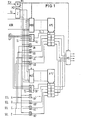
- FIG. 1 shows a fragmentary representation of a buffer memory with two flag field memories APS and APS ', in which the protective bits AP used for marking and monitoring individual cache entries are stored.
- These protection bits AP apply in the replacement algorithm in such a way that entries with the AP bit set are treated preferentially and protected against overwriting as long as there are still free memory locations with AP bits not set. This ensures a high hit rate for read access to protected information.
- a sensible use of these protection bits results, for example, from a preferred treatment of those memory accesses that take place in connection with address translation for virtual addresses. The lower the hit rate of the address translation memory itself, the more effective it is.
- the replacement algorithm can also be controlled in such a way that one AP bit is set per line in only one bank and thus only one entry is protected in order not to reduce the hit rate for normal accesses decrease very much.
- TCH time division multiplexing
- Flags M designed as a switching flip-flop, one or the other of the flag field memories APS, APS 'being alternately switched into the transmission path depending on the state of the two outputs M1, M2 of the flag.
- the flag M is controlled in such a way that the address ADR of a new memory entry, ie its page class address, reaches the flag field memory APS via the multiplexer MUS. Since the cache consists of four banks A, B, C, D, for example, four AND gates UA, UB, UC, UD are correspondingly present seen, which are driven on the one hand by the first output signal M1 of the flag M and on the other hand by the respective bank selection signal SEL A, SEL B, SEL C and SEL D. Because of the replacement algorithm chosen, according to which, for example, only one bank bit is to be set in each bank per line, for example only the AND gate UA is switched through, while the remaining AND gates are blocked.
- the setting of the respective AP bit in the flag field memory APS requires a clock pulse TI, which occurs at the output of a double AND gate DU.
- This clock signal TI arises from a logic operation in the upper part-AND gate of the double-AND gate, namely by linking the output signal M1 of the flag M pointing to the correct state with the AP signal sent by the processing unit and a read access load pulse LI .
- the lower part-AND gate of the double-AND gate DU is controlled by a clock signal TS and by the second state of the flag M via its output signal M2 and thus initially blocked.
- the four outputs of the flag field memory APS finally reach the replacement logic via a multiple switch MS, which is also controlled by the flag M, and which influences the replacement algorithm accordingly due to the new entry.
- the flag M is, as already mentioned, inverted on the basis of the signal TCH sent by the processing unit, with the result that now the second flag field memory APS 'is activated and the first one via the multiplexers MUX, MUX' and the multiple switch MS Flag field memory APS is locked.
- Both flag field memories APS and APS 'including the circuits associated with them stim The structure and function are completely the same, which is why the same reference numerals have been used for the second half of the circuit, but with an additional apostrophe.
- the second flag field memory APS When the second flag field memory APS 'is activated, a deletion process for the first flag field memory APS is initiated at the same time. This is done in that the cache is addressed line by line with the clock signal TS via a counter Z. The same clock signal TS goes to the clock input of the flag field memory APS via the lower part-AND gate of the double-AND gate UD, which has now been released by the flag M. Finally, all AND gates UA ... UD are blocked, so that zeros appear at the data inputs of banks, A, B, C, D.
- the sequential addressing of the entries with the aid of the counter Z controlled by the clock signal TS advantageously results in the fastest possible systematic resetting of the flag field memory.
- the clock signal TS can be derived, for example, from the machine clock.
- FIG. 2 shows a somewhat simplified circuit diagram compared to FIG. 1, the difference resulting from the absence of the counter Z and the two multiplexers MUX, MUX '.
- the lower part-AND gate of the double-AND gate is driven not by the clock signal TS but by the load pulse LI.
- the deletion process takes place in that the addresses ADR of each read access which does not lead to a hit in the cache are simultaneously used to delete the AP bits which are no longer current in the flag field memory APS '.
- a reset pulse is generated in the flag field memory APS 'at the same time, and the AP bit which may be present there is deleted.
- the reset here is no longer done systematically line by line, but depending on the randomness of the read accesses of the new program, it is correspondingly erratic and unsystematic.
- both flag field memories must of course be deleted when the system is switched on. This is expediently done by connecting both flag field memories in parallel and simultaneously deleting them with the aid of a clock signal, all entries being addressed sequentially by a counter present in the cache.
Landscapes
- Engineering & Computer Science (AREA)
- Theoretical Computer Science (AREA)
- Physics & Mathematics (AREA)
- General Engineering & Computer Science (AREA)
- General Physics & Mathematics (AREA)
- Memory System Of A Hierarchy Structure (AREA)
- Memory System (AREA)
Priority Applications (1)
| Application Number | Priority Date | Filing Date | Title |
|---|---|---|---|
| AT80105064T ATE13230T1 (de) | 1979-08-30 | 1980-08-26 | Schaltungsanordnung zum verarbeiten von daten in einer aus zentralprozessor, arbeitsspeicher und dazwischen angeordnetem pufferspeicher bestehenden datenverarbeitungsanlage. |
Applications Claiming Priority (2)
| Application Number | Priority Date | Filing Date | Title |
|---|---|---|---|
| DE2935135A DE2935135C2 (de) | 1979-08-30 | 1979-08-30 | Schaltungsanordnung zum Verarbeiten von Daten in einer aus Zentralprozessor, Arbeitsspeicher und dazwischen angeordnetem Pufferspeicher bestehenden Datenverarbeitungsanlage |
| DE2935135 | 1979-08-30 |
Publications (3)
| Publication Number | Publication Date |
|---|---|
| EP0024720A2 true EP0024720A2 (fr) | 1981-03-11 |
| EP0024720A3 EP0024720A3 (en) | 1982-08-11 |
| EP0024720B1 EP0024720B1 (fr) | 1985-05-08 |
Family
ID=6079678
Family Applications (1)
| Application Number | Title | Priority Date | Filing Date |
|---|---|---|---|
| EP80105064A Expired EP0024720B1 (fr) | 1979-08-30 | 1980-08-26 | Circuits pour le traitement de données dans un système de traitement de données comprenant un processeur central, une mémoire de travail et une mémoire tampon intercalée |
Country Status (3)
| Country | Link |
|---|---|
| EP (1) | EP0024720B1 (fr) |
| AT (1) | ATE13230T1 (fr) |
| DE (1) | DE2935135C2 (fr) |
Families Citing this family (2)
| Publication number | Priority date | Publication date | Assignee | Title |
|---|---|---|---|---|
| DE3207339A1 (de) * | 1982-03-02 | 1984-02-02 | ANT Nachrichtentechnik GmbH, 7150 Backnang | Schaltungsanordnung mit wenigstens zwei baugruppen |
| TWI775259B (zh) * | 2020-12-29 | 2022-08-21 | 新唐科技股份有限公司 | 直接記憶體存取裝置與使用其的電子設備 |
Family Cites Families (4)
| Publication number | Priority date | Publication date | Assignee | Title |
|---|---|---|---|---|
| JPS5440182B2 (fr) * | 1974-02-26 | 1979-12-01 | ||
| DE2605617A1 (de) * | 1976-02-12 | 1977-08-18 | Siemens Ag | Schaltungsanordnung zum adressieren von daten |
| US4070706A (en) * | 1976-09-20 | 1978-01-24 | Sperry Rand Corporation | Parallel requestor priority determination and requestor address matching in a cache memory system |
| US4229789A (en) * | 1977-12-22 | 1980-10-21 | Ncr Corporation | System for transferring data between high speed and low speed memories |
-
1979
- 1979-08-30 DE DE2935135A patent/DE2935135C2/de not_active Expired
-
1980
- 1980-08-26 EP EP80105064A patent/EP0024720B1/fr not_active Expired
- 1980-08-26 AT AT80105064T patent/ATE13230T1/de not_active IP Right Cessation
Also Published As
| Publication number | Publication date |
|---|---|
| DE2935135A1 (de) | 1981-03-12 |
| DE2935135C2 (de) | 1983-01-20 |
| EP0024720A3 (en) | 1982-08-11 |
| ATE13230T1 (de) | 1985-05-15 |
| EP0024720B1 (fr) | 1985-05-08 |
Similar Documents
| Publication | Publication Date | Title |
|---|---|---|
| DE3011552C2 (fr) | ||
| EP0013737B1 (fr) | Hiérarchie de mémoire à plusieurs étages pour un système de traitement des données | |
| DE3886182T2 (de) | Mehrcachedatenspeicheranordnung. | |
| DE3151745C2 (fr) | ||
| DE3588009T2 (de) | Vorrichtung und Verfahren zum Rekonfigurieren eines Speichers in einer Datenverarbeitungsanordnung. | |
| DE69329080T2 (de) | Cache-Speicher | |
| DE69721590T2 (de) | Ein bereichsbasiertes seiten-table-walk-bit verwendendes verfahren sowie vorrichtung | |
| DE2302074A1 (de) | Speicherschutzanordnung in einem multiprozessorsystem | |
| DE3618163C2 (de) | Speichermanagementanordnung für ein Mikroprozessorsystem | |
| DE68923863T2 (de) | Ein-/Ausgabecachespeicherung. | |
| EP0600112A1 (fr) | Système de traitement de données à adressage de mémoire virtuelle et clés de protection d'accès en mémoire | |
| DE3131341A1 (de) | "pufferspeicherorganisation" | |
| DE3502147C2 (fr) | ||
| DE2939411C2 (de) | Datenverarbeitungsanlage mit virtueller Speicheradressierung | |
| DE3046912C2 (de) | Schaltungsanordnung zum selektiven Löschen von Cachespeichern in einer Multiprozessor-Datenverarbeitungsanlage | |
| DE2432608A1 (de) | Speicheranordnung fuer datenverarbeitungseinrichtungen | |
| DE3911721C2 (fr) | ||
| EP0024720B1 (fr) | Circuits pour le traitement de données dans un système de traitement de données comprenant un processeur central, une mémoire de travail et une mémoire tampon intercalée | |
| DE3832758A1 (de) | Computerisierte arbeitsstation | |
| DE3588166T2 (de) | Entwurf einer Cache-Hierarchie zur Anwendung in einer Speicherverwaltungseinheit | |
| DE2605617A1 (de) | Schaltungsanordnung zum adressieren von daten | |
| DE3887862T2 (de) | Cache-Speichervorrichtung. | |
| EP0257405B1 (fr) | Procédé et dispositif de mise à jour de combinaisons de bits de contrôle | |
| DE3009317A1 (de) | Hybrid-assoziativspeicher | |
| DE68921869T2 (de) | Ein-/Ausgabebuscachespeicherung. |
Legal Events
| Date | Code | Title | Description |
|---|---|---|---|
| PUAI | Public reference made under article 153(3) epc to a published international application that has entered the european phase |
Free format text: ORIGINAL CODE: 0009012 |
|
| AK | Designated contracting states |
Designated state(s): AT BE CH FR GB IT LU NL SE |
|
| 17P | Request for examination filed |
Effective date: 19811028 |
|
| PUAL | Search report despatched |
Free format text: ORIGINAL CODE: 0009013 |
|
| AK | Designated contracting states |
Designated state(s): AT BE CH FR GB IT LU NL SE |
|
| GRAA | (expected) grant |
Free format text: ORIGINAL CODE: 0009210 |
|
| AK | Designated contracting states |
Designated state(s): AT BE CH FR GB IT LI LU NL SE |
|
| PG25 | Lapsed in a contracting state [announced via postgrant information from national office to epo] |
Ref country code: IT Free format text: LAPSE BECAUSE OF FAILURE TO SUBMIT A TRANSLATION OF THE DESCRIPTION OR TO PAY THE FEE WITHIN THE PRESCRIBED TIME-LIMIT;WARNING: LAPSES OF ITALIAN PATENTS WITH EFFECTIVE DATE BEFORE 2007 MAY HAVE OCCURRED AT ANY TIME BEFORE 2007. THE CORRECT EFFECTIVE DATE MAY BE DIFFERENT FROM THE ONE RECORDED. Effective date: 19850508 |
|
| ET | Fr: translation filed | ||
| PG25 | Lapsed in a contracting state [announced via postgrant information from national office to epo] |
Ref country code: LU Free format text: LAPSE BECAUSE OF NON-PAYMENT OF DUE FEES Effective date: 19850831 |
|
| PLBE | No opposition filed within time limit |
Free format text: ORIGINAL CODE: 0009261 |
|
| STAA | Information on the status of an ep patent application or granted ep patent |
Free format text: STATUS: NO OPPOSITION FILED WITHIN TIME LIMIT |
|
| 26N | No opposition filed | ||
| PGFP | Annual fee paid to national office [announced via postgrant information from national office to epo] |
Ref country code: AT Payment date: 19860805 Year of fee payment: 7 |
|
| PGFP | Annual fee paid to national office [announced via postgrant information from national office to epo] |
Ref country code: NL Payment date: 19860831 Year of fee payment: 7 |
|
| PG25 | Lapsed in a contracting state [announced via postgrant information from national office to epo] |
Ref country code: AT Effective date: 19870826 |
|
| PG25 | Lapsed in a contracting state [announced via postgrant information from national office to epo] |
Ref country code: SE Effective date: 19870827 |
|
| PG25 | Lapsed in a contracting state [announced via postgrant information from national office to epo] |
Ref country code: LI Effective date: 19870831 Ref country code: CH Effective date: 19870831 |
|
| BERE | Be: lapsed |
Owner name: SIEMENS A.G. BERLIN UND MUNCHEN Effective date: 19870831 |
|
| PG25 | Lapsed in a contracting state [announced via postgrant information from national office to epo] |
Ref country code: NL Effective date: 19880301 |
|
| NLV4 | Nl: lapsed or anulled due to non-payment of the annual fee | ||
| PG25 | Lapsed in a contracting state [announced via postgrant information from national office to epo] |
Ref country code: FR Free format text: LAPSE BECAUSE OF NON-PAYMENT OF DUE FEES Effective date: 19880429 |
|
| REG | Reference to a national code |
Ref country code: CH Ref legal event code: PL |
|
| GBPC | Gb: european patent ceased through non-payment of renewal fee | ||
| REG | Reference to a national code |
Ref country code: FR Ref legal event code: ST |
|
| PG25 | Lapsed in a contracting state [announced via postgrant information from national office to epo] |
Ref country code: GB Free format text: LAPSE BECAUSE OF NON-PAYMENT OF DUE FEES Effective date: 19881118 |
|
| PG25 | Lapsed in a contracting state [announced via postgrant information from national office to epo] |
Ref country code: BE Effective date: 19890831 |
|
| EUG | Se: european patent has lapsed |
Ref document number: 80105064.2 Effective date: 19880707 |