EP0025171A2 - Circuit pour la mesure de distances commandée par un capteur, pourvu d'un dispositif de mesure de la lumière - Google Patents
Circuit pour la mesure de distances commandée par un capteur, pourvu d'un dispositif de mesure de la lumière Download PDFInfo
- Publication number
- EP0025171A2 EP0025171A2 EP80105060A EP80105060A EP0025171A2 EP 0025171 A2 EP0025171 A2 EP 0025171A2 EP 80105060 A EP80105060 A EP 80105060A EP 80105060 A EP80105060 A EP 80105060A EP 0025171 A2 EP0025171 A2 EP 0025171A2
- Authority
- EP
- European Patent Office
- Prior art keywords
- sensor
- sensor elements
- sensor element
- comparison
- circuit
- Prior art date
- Legal status (The legal status is an assumption and is not a legal conclusion. Google has not performed a legal analysis and makes no representation as to the accuracy of the status listed.)
- Granted
Links
- 238000005259 measurement Methods 0.000 title claims abstract description 12
- 230000010354 integration Effects 0.000 claims abstract description 12
- 238000011156 evaluation Methods 0.000 claims abstract description 11
- 239000004065 semiconductor Substances 0.000 claims description 22
- 239000003990 capacitor Substances 0.000 claims description 8
- 238000009413 insulation Methods 0.000 claims description 3
- 238000000034 method Methods 0.000 abstract description 2
- 230000003287 optical effect Effects 0.000 description 4
- 238000013461 design Methods 0.000 description 3
- 238000005516 engineering process Methods 0.000 description 3
- 238000012546 transfer Methods 0.000 description 3
- 101000847024 Homo sapiens Tetratricopeptide repeat protein 1 Proteins 0.000 description 2
- 102100032841 Tetratricopeptide repeat protein 1 Human genes 0.000 description 2
- 101150054429 Tprn gene Proteins 0.000 description 2
- 239000002800 charge carrier Substances 0.000 description 2
- 230000001419 dependent effect Effects 0.000 description 2
- 238000010586 diagram Methods 0.000 description 2
- 238000006073 displacement reaction Methods 0.000 description 2
- 108010076504 Protein Sorting Signals Proteins 0.000 description 1
- 229910004298 SiO 2 Inorganic materials 0.000 description 1
- 230000008901 benefit Effects 0.000 description 1
- 230000000903 blocking effect Effects 0.000 description 1
- 230000008859 change Effects 0.000 description 1
- 238000006880 cross-coupling reaction Methods 0.000 description 1
- 230000007423 decrease Effects 0.000 description 1
- 238000011161 development Methods 0.000 description 1
- 230000018109 developmental process Effects 0.000 description 1
- 230000006870 function Effects 0.000 description 1
- 238000003384 imaging method Methods 0.000 description 1
- 239000002184 metal Substances 0.000 description 1
- 238000001208 nuclear magnetic resonance pulse sequence Methods 0.000 description 1
- 229910021420 polycrystalline silicon Inorganic materials 0.000 description 1
- 238000005036 potential barrier Methods 0.000 description 1
- 229910052710 silicon Inorganic materials 0.000 description 1
- 239000010703 silicon Substances 0.000 description 1
Images




Classifications
-
- H—ELECTRICITY
- H10—SEMICONDUCTOR DEVICES; ELECTRIC SOLID-STATE DEVICES NOT OTHERWISE PROVIDED FOR
- H10F—INORGANIC SEMICONDUCTOR DEVICES SENSITIVE TO INFRARED RADIATION, LIGHT, ELECTROMAGNETIC RADIATION OF SHORTER WAVELENGTH OR CORPUSCULAR RADIATION
- H10F39/00—Integrated devices, or assemblies of multiple devices, comprising at least one element covered by group H10F30/00, e.g. radiation detectors comprising photodiode arrays
- H10F39/10—Integrated devices
- H10F39/12—Image sensors
- H10F39/15—Charge-coupled device [CCD] image sensors
- H10F39/158—Charge-coupled device [CCD] image sensors having arrangements for blooming suppression
Definitions
- the invention relates to a circuit provided with an exposure measuring part for sensor-controlled distance measurement according to the preamble of patent claim 1.
- the invention has for its object to solve the aforementioned difficulties in a circuit of the type mentioned. This object is achieved by the features characterized in claim 1.
- the advantage that can be achieved with the invention is, in particular, that an overflow current caused by a highly uneven exposure of a linear image sensor influences the evaluator connected downstream of the comparison sensor element and thus ends the integration time in such a way that on the one hand there is no overflow of charge from the excessively strong irradiated sensor elements comes into the neighboring elements and that the optically generated charges accumulated in the less exposed sensor elements lie significantly below the reference charges.
- the circuit shown in Fig. 1 contains two linear image sensors 1 and 2, which are equipped with sensor elements 11, 12 ... 1n and 21, 22 ... 2n.
- the image sensors 1, 2 are integrated on a doped semiconductor body of a first conductivity type. If the sensor elements are implemented as photodiodes, the hatched rectangles represent regions of an area opposite to the first, second conductivity type arranged at an interface of the semiconductor body.
- the sensor elements 11 ... 1n and 21 ... 2n are individually assigned in series Switching transistors T11 ... T1n and T31 ... T3n or T21 ... T2n and T41 ... T4n are connected to connections that are connected to a supply voltage U DD .
- T1n and T21 ... T2n are each connected to a common connection to which a clock pulse voltage ⁇ 1 is supplied.
- the sensor elements 11 ... 1n and 21 ... 2n are connected to the inputs of evaluators 31 ... 3n via the switching transistors T31 ... T3n and T41 ... T4n, whose gate electrodes are connected to a common clock pulse voltage ⁇ 62 and 41 ... 4n connected.
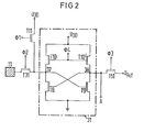
- evaluators 31 ... 3n and 41 ... 4n An expedient circuit design of evaluators 31 ... 3n and 41 ... 4n will be described in more detail with reference to FIG. 2. Further inputs of these evaluators are connected to connections which are connected to a reference voltage U Ref via common switching transistors T51 and T52, the gate electrodes of which are connected to a clock pulse voltage ⁇ 3.
- the evaluators 31 ... 3n and 41 ... 4n can, depending on the Voltages supplied to them via switching transistors T31 ... T3n and T41 ... T4n assume one of two possible switching states.
- Their output signals S11 ... S1n and S21 ... S2n which correspond to the logic voltage level "1" or "0" depending on the switching state assumed, are transferred via transfer transistors T61 ...
- the shift register 5 has two inputs which are connected to clock pulse voltages ⁇ 1L and ⁇ 2L, while the shift register 6 has two inputs to which the clock pulse voltages ⁇ 1R and 02R are supplied.
- the output 5a of the stage 5n is connected on the one hand via a line 5b to the input of the stage 51 and on the other hand to a first input of a logic circuit 8 arranged in an evaluation part 7.
- the output 6a of the stage 6n is led in a corresponding manner via a line 9 to the input of the stage 61 and, on the other hand, is connected to a second input of 8.
- the logic circuit 8 is followed by a counter 10, the output of which is connected to the first input of a digital comparator 13 and via an electronic switch 14 to a memory 15. The output of the memory 15 is led to a second input of the digital comparator 13.
- a clock pulse generator 16 is provided with outputs for the clock pulse voltages ⁇ 1 to ⁇ 63 and ⁇ 5.
- the clock pulse chip is via further outputs 17 and 18 Solutions ⁇ 1L and ⁇ 62L as well as ⁇ 1R and 02R, whereby a gate circuit 19 is arranged in series with the outputs 17 and a gate circuit 20 is arranged in series with the outputs 18.
- the control inputs of 19 and 20 are acted upon via lines 23 and 24 with control signals to be described in more detail.
- the clock pulse generator has a further output 25, to which a further gate circuit 26 is arranged in series. This is assigned a further control signal via a line 27.
- the output 25 is connected to the input of a counter 28, the output of which is connected to a memory 30 via an electronic switch 29.
- the output 33 of the memory 30 is connected to a device 34 described below.
- a strip-shaped comparison sensor element 111 is arranged, the longitudinal axis of which is aligned with a line running parallel to the image sensor 1.
- the comparison sensor element is implemented as a photodiode, the area hatched in FIG. 1 corresponding to the lateral dimensions of a redoped area of the semiconductor body.
- the between the sensor elements 11 ... 1n and the comparison sensor element 111 lying 'region of the semiconductor body is covered by a acted upon with a constant voltage U G gate G, which is separated from the boundary surface of the semiconductor body by a thin insulating layer.
- the comparison sensor element 111 is connected via a switching transistor T111 to a connection which is connected to the supply voltage U DD .
- the clock pulse voltage 01 is supplied to the gate of the transistor T111.
- the comparison sensor element 111 is ver with the input of an evaluator 131 bound, which corresponds to the evaluators 31 ... 3n and 41 ... 4n in structure.
- the evaluator 131 is supplied with the reference voltage U Ref via a switching transistor T151 to which a clock pulse voltage ⁇ 3 'is applied.
- the output 131a of the evaluator 131 is connected to the control input of a gate circuit 116. This is arranged in series with an output 115 of the clock pulse generator 16, at which the clock pulse voltage 02 can be tapped.
- the circuit parts G, 111, T111, 131 and T151 represent the exposure measuring part of the circuit, the output of which is formed by 131a.
- FIG. 2 shows an expedient embodiment of the evaluators 31 ... 3n, 41 .- .. 4n and 131 based on the evaluator 31. It consists of a flip-flop circuit with the switching transistors T8 and T9 and the transistors operated as switchable load elements T10 and T10 '.
- the source connections of T8 and T9 are connected via a common connection 35 to the reference potential of the circuit, the drain connections of T10 and T10 'via a common connection to the supply voltage U DD .
- the input node of the evaluator 31 is designated 37, the output node 38. There is a cross coupling between the gate electrodes of T8 and T9 and the nodes 37 and 38.
- the gate electrodes of T10 and T10 'of the evaluators 31 ... 3n and 41 ... 4n are connected to a clock pulse voltage 04 via a common connection.
- the circuit parts T11, 11 and T31 and T51 connected to nodes 37 and 38 have already been described with reference to FIG. 1.
- the principle of distance measurement of an object used in the invention assumes that two separate images are obtained from it via two optical devices, the distance-dependent ones of which Relative positions are evaluated.
- the light rays L1 in FIG. 1 emanate from the object to be determined in its distance. They project an image of the same onto the plane of the image sensor 1 via a first optical device in such a way that it is aligned with a line section of the image.
- the light beams L2 which are obtained from the object via a second optical device, project a second image thereof onto the end of the image sensor 2, in such a way that it is directed onto the same line section when the object is in a predetermined distance, for example at an "infinite" distance.
- the line sections projected onto the image sensors 1 and 2 accordingly shift in the longitudinal direction of the image sensors.
- the size of the mutual displacement represents a measure of the actual distance of the object.
- the mode of operation of the circuit according to FIGS. 1 and 2 results in connection with the pulse-time diagrams according to FIG.
- the sensor elements, for example 11, and the input nodes, for example 37, are thus evaluated by the evaluators 31 ... 3n and 41 ... 4n conductive transistors, such as T11 and T31, reset to the supply voltage U DD .
- a simultaneously starting clock pulse ⁇ 3 switches T51 into the conductive state, so that the output node 38 is connected to the reference voltage U Ref .
- the clock pulse ⁇ 1 is switched off, charge carriers generated by the incident light beams L1 or L2 begin to accumulate in the sensor elements, for example 11, a voltage drop occurring in the sensor elements. The larger the optically generated charges accumulated in the sensor elements 11 ... 1n and 21 ...
- the time period between the end of the clock pulse ⁇ 1 at the time t1 and the end of the clock pulse ⁇ 2 at the time t2 is referred to as the integration time T i . Only within this period of time do optically generated charges accumulate in the sensor elements.
- a clock pulse ⁇ 4 which can be tapped at a further output of the clock pulse generator, is applied to the gate electrodes of T10 and T10 ', so that the flip-flop circuits of the evaluators 31 ... 3n and 41 ... 4n can be activated.
- a voltage approximately corresponds to the supply voltage U DD (logic "1"). If, on the other hand, the voltage at node 37 does not fall below U Ref , node 38 reaches a potential which corresponds approximately to the reference potential at terminal 35 (logic "0").
- each evaluator emits a digitized sensor signal, e.g. S11, the value of which depends on when it is reached or failure to reach a reference charge in the individual sensor elements which is present when the potential at node 37 at time t2 equals the potential of node 38 reset to voltage U Ref .
- a digitized sensor signal e.g. S11
- the circuit parts G, 111, T111, 131 and T151 are used to determine the optimal integration time.
- the comparison sensor element 111 collects after the time t1, i.e. after the rear flank of ⁇ 1 ', an optically generated charge, which corresponds in each case to the mean value of the exposure of all sensor elements 11 ... 1n, which are located next to the comparison sensor element 111. Since this average value with a very strong exposure of a small part of the sensor element line 11 ...
- the reference charge in which the evaluator 131 is switched to the switching state by emitting a logic output signal "1"
- the overflowing charge parts With an extremely strong exposure of some sensor elements, in which there is an overflow of parts of the accumulated, optically generated charges from the affected sensor elements, the overflowing charge parts now overcome the potential threshold existing below the gate G and reach the comparison sensor element 111, the Charge content is greatly increased, so that the reference charge is reached much faster than before.
- the chip decreases voltage U111 on the same starting from the reset value U DD (Fig. 3). If the evaluator 131, which is activated during the occurrence of a clock pulse ⁇ 4v, is supplied with U Ref via the transistor 151 during the occurrence of the clock pulses ⁇ 3v, the voltage U Ref for the clock pulse ⁇ 3v for U111 is already undercut has, the switchover of the evaluator 131 to the output signal "1". This blocks the gate circuit 116 and ends the pulse 02, which means that the end of the integration time for the sensor elements 11 ... 1n and 21 ... 2n is given.
- the digitized sensor signals output by evaluators 31 ... 3n and 41 ... 4n, e.g. S11, the inputs of the assigned stages, e.g. 51, the shift registers 5 and 6 are fed and stored in these.
- the clock pulse generator 16 then delivers clock pulse sequences ⁇ 1L, ⁇ 2L, ⁇ 1R and ⁇ 2R, which each shift the information contained in the stages of the shift registers 5 and 6 by one stage.
- the sensor signal S1n appears at the output 5a.
- the clock pulses 43 and 44 shift the information S1n to stage 51 and the information S1 (n-1) to output 5a, and so on.
- the clock signals 45 and 46 of the clock period TPLn finally return the sensor signal S1n to the output 5a after a complete circulation of information.
- the clock pulses 53 and 54 shift the T clock period TPL1 'the sensor signals again by one stage, so that Sl (n-1) reaches stage 51 and S1 (n-2) is switched through to output 5a.
- a first readout cycle Z1 which includes the clock periods TPL1 to TPLn
- the sensor signals S1n to S1 and again S1n are output serially at the output 5a.
- a second read cycle Z2 which includes the clock period TPL1 'and n-1 further clock periods
- the shift register 6 is also acted upon by n clock periods TPR1 to TPRn, while the corresponding clock pulses 47 and 48 are missing pulses.
- the sensor signal S2n is present at the output 6a and the signal S1 (n-1) is present at the output 5a at the beginning of Z2.
- the signal pairs S1n and S2n, S1 (n-1) and S2 (n-1) etc. are read out serially at 5a and 6a, in the second read cycle, however, the signal pairs S1 (n-1) and S2n, S1 (n-2) and S2 (n-1) etc.
- the serially read information of the shift registers 5 and 6 are thus shifted from one another by one signal width in two successive read cycles. After n read cycles, they then have the same time assignment as in cycle Z1. In Fig. 1 this shift can be achieved in that the gate circuit 20 is blocked via the line 24 during the occurrence of the clock pulses 47 and 48, ie between the clock periods .TPRn and TPR1 '.
- the gate circuit 26 can be opened via the control line 27, so that one of the pulses 47 or 48 or one of these derived pulse appears at output 25 as shift pulse P1.
- This shift pulse P1 marks the beginning of a new read cycle and a mutual shift of the sensor signals read out serially at the outputs 5a and 6a by one signal width each.
- read sensor signal pairs are evaluated in the logic circuit 8 according to the exclusive-OR function.
- An output pulse occurs at output 55 of FIG. 8 whenever the digital signals supplied via 5a and 6a match. If they do not match, no output pulse is emitted from 8.
- the subcircuit 8 can also be designed such that it only indicates the correspondence of two "1" signals or two "0" signals at its inputs by an output pulse.
- the counter 10 which is reset to zero before the start of each readout cycle, that is to say in the blanking gaps 49, then counts the number of matches within such a cycle.
- the counter 10 is only activated during part of each read cycle, which is determined by one of 16 emitted pulses ⁇ F. Assuming that the counter 10 in the readout cycle Z1 counts the matches within the clock periods TPRi to TPR k , the difference ki being approximately n / 2 or 3n / 4, it counts in the readout cycle Z2 the matches within the clock periods TPR i + 1 to TPR ' k + 1 If one considers the pulses ⁇ F1 and ⁇ F2 as "readout windows", the sensor signals of shift register 6 in window ⁇ F2 are one signal width to the left compared to window ⁇ F1 (Fig. 3) postponed.
- the signals of 5 in the "window” OF3 I have shifted by a signal width to the right. If the "window” is generally shifted to the right in the first readout cycle Z1 and in the further readout cycles Z3, Z5, Z7, etc., this corresponds to an alternating shift of the sensor signal sequences tapped at 6a or 5a in the respective window ⁇ F one signal width to the left or right. Those pulses ⁇ 6F which would enclose the evaluation signals derived from the beginning and end of one of the sensor element lines at the same time are suppressed by the clock pulse generator 16. This ensures that the "windows” ⁇ F switch off the evaluation of those sensor signals which have been derived from the start and end sections of the projected line sections, which are interchanged, so that they provide no information about the actual brightness curve along the line section .
- the switch 29 Since the switch 29 is actuated in synchronism with the switch 14, it always transmits the new counter reading from 28 to the memory 30 whenever a larger counting result occurs in the counter 10.
- the number of shifting pulses Pi is thus stored in the memory 30 after n information cycles characterizes such a shift in information between the sensor signals of the shift registers 5 and 6 in which the greatest number of matches occurs.
- the number of shift pulses P1, P2 etc. stored in the memory 30 gives off that relative shift of the sensor signals circulating in the shift registers 5 and 6, for which there is a maximum correlation of the sensor signals compared with one another.
- the blanking gaps 49 indicated in Fig. 3, e.g. required to reset the counter 10 to zero in each case are generated by a corresponding blocking of the gate circuits 19 and 20 via their control lines 23 and 24.
- the digital signal occurring at the output 33 of the memory 30 is fed to a device 34 which can be regarded as a display device which, after corresponding coding of the digital signal, provides a digital or analog display of the distance of the object.
- the device 34 can also consist of a known adjustment device of a photographic or electronic camera, which is the distance of one from one Movable lens image plane so that the object is sharply imaged on this image plane.
- a device of this type is described, for example, in German patent application P 28 13 915.3 (VPA 78 P 7025) and in the magazine "Electronics" from Nov. 10, 1977 on pages 40 to 44.
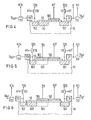
- a thin, electrically insulating layer 59 for example made of SiO 2 , is provided on a doped semiconductor body 58, for example made of p-doped silicon.
- the image sensor 11 is designed as a photodiode, which consists of the n-doped semiconductor region 60. This area also forms the source area of the transistor T31 (FIG. 1).
- the gate of T31 is arranged on the insulating layer 59 and is designated by 160.
- the drain region of T31 bears the reference symbol 161.
- the region 161 is connected on the one hand via the transistor T11 to a connection which is connected to the supply voltage UDD, and on the other hand forms the input of the evaluator 31 or the drain region of the transistor T8 provided therein Fig. 2) and the source region of the transistor T10.
- the second input of 31 is connected via the transistor T51 with ⁇ 63 to a connection which is connected to the reference voltage U Ref .
- the comparison sensor element 111 is designed as a photodiode consisting of the n-doped region 162.
- the area 162 is connected on the one hand via the transistor T111 with 01 to a connection which is connected to U DD , and on the other hand to the first input of the evaluator 131, the second input of which is connected to a train with 73v sistor T151 is at the reference voltage U Rei .
- FIG. 5 An alternative circuit to FIG. 4 is shown in FIG. 5.
- the sensor element 11 then consists of an MIS capacitor (metal insulation layer semiconductor capacitor) which has a gate 165 which is arranged on the insulation layer 59.
- the gate 165 is manufactured, for example, from highly doped polycrystalline silicon and is connected to a clock pulse voltage ⁇ K, under the influence of which a space charge zone 166 forms in the semiconductor body 58.
- the other circuit parts of FIG. 5 correspond to the circuit parts of FIG. 4 which have been given the same reference numerals, it being pointed out that the transistor T11 has a clock pulse voltage ⁇ 1 'and the transistor T31 has a clock pulse voltage ⁇ 2'.
- the clock pulses ⁇ 1 ', 02' and ⁇ K which begin at the same time, cause the MIS capacitor in the region of the interface 58a of the semiconductor body 58 to be reset to the value of the supply voltage U DD by the time t1.
- the integration time in which optically generated charge carriers are collected begins in the MIS capacitor which continues to be supplied with ⁇ K.
- the end of the integration time has also been reached.
- a new clock pulse ⁇ 2' is applied so that a charge transfer from 166 to 161, indicated by the arrow 504 (FIG. 3), can take place causes a corresponding change in potential at the input of the evaluator 31.
- the gate G here lies between the region 162 and the gate 165 of the MIS capacitor.
- FIG. 6 differs from FIG. 5 only in that a photodiode 601 is arranged next to the MIS capacitor 165, 166, on the side thereof remote from T31.
- the gate electrode of T31 is connected to the pulse voltage ⁇ 2 ', while the gate electrode of T11 is supplied with the clock pulse voltage ⁇ 1'.
- the gate G lies between the regions 162 and 601.
- the capacitance of the sensor element 11 according to FIG. 5 is greater than the capacitance of the sensor element according to FIG. 4, while the capacitance of the sensor element 11 according to FIG. 6 is larger than that according to the embodiment Fig. 5.
- FIG. 7 shows a second exemplary embodiment of the invention, in which two circuits according to FIG. 1 are provided with a common evaluation part 7 and common devices 34 connected downstream thereof.
- the components of the subcircuit arranged on the left side of the evaluation part 7 in FIG. 1 are provided with the same reference numerals in FIG. 7.
- the individual sensor elements 11, 12 ... 1n are so narrow in the longitudinal direction of the image sensor 1 that they correspond approximately to half the dimensions of the evaluators 31, 32 ... 3n.
- the switching transistors T11 etc., T31 etc., T61 etc., T111 etc., and T151 were also included in these evaluators for the sake of simplicity of illustration.
- the corresponding components of the second circuit according to FIG. 1 are each provided with reference numerals in FIG.
- the sensor elements 12 ... 1n of the an image sensor is arranged in the gaps between the sensor elements 11 ', 12' ... 1n 'of the other image sensor.
- the sensor elements are divided in the middle, their parts being connected to each other with a conductive bridge, for example LB.
- twice the number of sensor elements can be accommodated on a sensor length corresponding to FIG. 1, so that the resolution of the line sections projected onto the sensor elements is substantially greater than in FIG. 1.
- alternately operable electronic switches 5c and 5c' are provided which alternately connect one of the outputs 5a and 5a 'to one input of the logic circuit 8 and to the input of the relevant first stage 51 or 51' of the shift registers. They are controlled by means of clock pulse voltages 06 and 06 '.
- the clock periods of 06 are separated from one another by equally long intermediate periods. With these intermediate periods, the clock periods of ⁇ 6 'coincide.
- the evaluation part 7 is to be supplemented on the right-hand side by the evaluation part 7 by a corresponding arrangement of two further image sensors 2 and 2 'and the evaluators and shift registers assigned to them, the sensor elements of which are also so narrow that they are in the longitudinal direction of the image sensors 2 or 2 'correspond to half the evaluator width.
- Fig. 8 finally shows a circuit corresponding to Fig. 1, in which the image sensors 1 and 2 are arranged side by side, so that their sensor elements 11, 12 ... In and 21, 22 ... 2n lie in two adjacent lines.
- the evaluators 31, 32 ... 3n and 41, 42 ... 4n each also contain the switching transistors T11 etc. to T71 etc., the evaluators 131 ... 13n, the transistors T111 etc. and T151.
- This exemplary embodiment can be used if the images of the object are only projected halfway onto the plane of the image sensors of FIGS.
- the circuits described and illustrated can particularly advantageously be fully or partially integrated monolithically on a doped semiconductor body.
- the semiconductor body for example 58, is preferably of p-type design and the rest of the circuit structure is implemented using MOS n-channel technology.
- the semiconductor body is at a reference potential, the voltages and potentials given having a positive sign in relation to this.
- a n-type semiconductor bodies and a MOS p-channel technology make these signs negative.
Landscapes
- Automatic Focus Adjustment (AREA)
- Measurement Of Optical Distance (AREA)
- Focusing (AREA)
- Viewfinders (AREA)
- Transforming Light Signals Into Electric Signals (AREA)
- Length Measuring Devices By Optical Means (AREA)
- Solid State Image Pick-Up Elements (AREA)
Applications Claiming Priority (2)
| Application Number | Priority Date | Filing Date | Title |
|---|---|---|---|
| DE2936536 | 1979-09-10 | ||
| DE19792936536 DE2936536A1 (de) | 1979-09-10 | 1979-09-10 | Mit einem belichtungsmessteil versehene schaltung zur sensorgesteuerten entfernungsmessung |
Publications (3)
| Publication Number | Publication Date |
|---|---|
| EP0025171A2 true EP0025171A2 (fr) | 1981-03-18 |
| EP0025171A3 EP0025171A3 (en) | 1982-09-01 |
| EP0025171B1 EP0025171B1 (fr) | 1985-12-18 |
Family
ID=6080494
Family Applications (1)
| Application Number | Title | Priority Date | Filing Date |
|---|---|---|---|
| EP80105060A Expired EP0025171B1 (fr) | 1979-09-10 | 1980-08-26 | Circuit pour la mesure de distances commandée par un capteur, pourvu d'un dispositif de mesure de la lumière |
Country Status (4)
| Country | Link |
|---|---|
| US (1) | US4334151A (fr) |
| EP (1) | EP0025171B1 (fr) |
| JP (1) | JPS5646408A (fr) |
| DE (1) | DE2936536A1 (fr) |
Cited By (3)
| Publication number | Priority date | Publication date | Assignee | Title |
|---|---|---|---|---|
| EP0057259A1 (fr) * | 1981-01-30 | 1982-08-11 | Siemens Aktiengesellschaft | Circuit pour coder en binaire des signaux détecteurs d'un nombre d'éléments sensibles optoélectroniques et procédé pour le faire fonctionner |
| EP0275217A3 (fr) * | 1987-01-16 | 1989-12-13 | Canon Kabushiki Kaisha | Dispositif de conversion photovoltaique |
| AU771324B2 (en) * | 2000-04-07 | 2004-03-18 | Kabushiki Kaisha Toshiba | System for controlling power plants and method for arranging the system |
Families Citing this family (15)
| Publication number | Priority date | Publication date | Assignee | Title |
|---|---|---|---|---|
| JPS5764713A (en) * | 1980-10-09 | 1982-04-20 | Mamiya Koki Kk | Automatic focus controller |
| US4635126A (en) * | 1981-12-18 | 1987-01-06 | Canon Kabushiki Kaisha | Image pick-up system |
| US4490036A (en) * | 1982-08-18 | 1984-12-25 | Eastman Kodak Company | Image sensor and rangefinder device having background subtraction with paired analog shift registers |
| US4636624A (en) * | 1983-01-10 | 1987-01-13 | Minolta Camera Kabushiki Kaisha | Focus detecting device for use with cameras |
| US5202555A (en) * | 1983-01-10 | 1993-04-13 | Minolta Camera Kabushiki Kaisha | Focus detecting device for use with cameras with correlation and contrast detecting means |
| FR2539568B1 (fr) * | 1983-01-14 | 1987-12-11 | Asahi Optical Co Ltd | Dispositif analyseur d'images a semi-conducteurs |
| US4583002A (en) * | 1983-06-06 | 1986-04-15 | Fuji Photo Film Co., Ltd. | Imaging sensor with automatic sensitivity control comprising voltage multiplying means |
| US4758082A (en) * | 1985-04-17 | 1988-07-19 | Canon Kabushiki Kaisha | Distance detection apparatus |
| JP2563370B2 (ja) * | 1986-12-27 | 1996-12-11 | オリンパス光学工業株式会社 | 焦点検出用光電変換装置 |
| DE4042529C2 (de) * | 1989-05-09 | 1995-07-27 | Asahi Optical Co Ltd | Kamera mit Varioobjektiv, Autofokus-Einrichtung und Hilfslichtprojektionssystem |
| US5291044A (en) * | 1990-12-12 | 1994-03-01 | Eastman Kodak Company | Image sensor with continuous time photodiode |
| JPH09226416A (ja) * | 1996-02-20 | 1997-09-02 | Yazaki Corp | 電装モジュールの組付け構造 |
| DE19710722C2 (de) * | 1996-03-15 | 2003-06-05 | Pentax Corp | Automatische Fokussiereinrichtung für ein Fernrohr |
| DE19730976C2 (de) * | 1996-07-19 | 2003-12-24 | Pentax Corp | Einrichtung zum Scharfstellen des Objektivs einer Kamera |
| DE102016213913A1 (de) * | 2016-07-28 | 2018-02-01 | Robert Bosch Gmbh | Sensorvorrichtung für ein Fahrzeug, Fahrzeug, Verfahren zum Betreiben einer Sensorvorrichtung |
Family Cites Families (11)
| Publication number | Priority date | Publication date | Assignee | Title |
|---|---|---|---|---|
| FR2015256A1 (fr) * | 1968-08-08 | 1970-04-24 | Eastman Kodak Co | |
| DE2225557A1 (de) * | 1971-06-23 | 1973-03-15 | Hauser Raimund | Entfernungsmesser |
| US3931465A (en) * | 1975-01-13 | 1976-01-06 | Rca Corporation | Blooming control for charge coupled imager |
| JPS5374424A (en) * | 1976-12-15 | 1978-07-01 | Asahi Optical Co Ltd | Photoelectric detection device suited for detecting focal point |
| JPS5385454A (en) * | 1977-01-06 | 1978-07-27 | Canon Inc | Distance detecting method |
| JPS53110823A (en) * | 1977-03-10 | 1978-09-27 | Ricoh Co Ltd | Optical information processor |
| DE2847368A1 (de) * | 1977-11-02 | 1979-05-03 | Canon Kk | Kamera mit automatischer scharfeinstellvorrichtung |
| DE2813913A1 (de) * | 1978-03-31 | 1979-10-18 | Siemens Ag | Anordnung zur messung der entfernung oder geschwindigkeit eines gegenstandes |
| JPS54130825A (en) * | 1978-03-31 | 1979-10-11 | Canon Inc | Image scanner |
| DE2813915A1 (de) | 1978-03-31 | 1979-10-11 | Siemens Ag | Anordnung zur scharfeinstellung der abbildung eines gegenstandes auf eine bildebene |
| DE2838647A1 (de) * | 1978-09-05 | 1980-04-10 | Siemens Ag | Verfahren zur automatischen oder halbautomatischen entfernungsmessung und scharfeinstellung der abbildung eines gegenstandes auf eine bildebene |
-
1979
- 1979-09-10 DE DE19792936536 patent/DE2936536A1/de active Granted
-
1980
- 1980-07-11 US US06/168,649 patent/US4334151A/en not_active Expired - Lifetime
- 1980-08-26 EP EP80105060A patent/EP0025171B1/fr not_active Expired
- 1980-09-09 JP JP12522280A patent/JPS5646408A/ja active Granted
Cited By (3)
| Publication number | Priority date | Publication date | Assignee | Title |
|---|---|---|---|---|
| EP0057259A1 (fr) * | 1981-01-30 | 1982-08-11 | Siemens Aktiengesellschaft | Circuit pour coder en binaire des signaux détecteurs d'un nombre d'éléments sensibles optoélectroniques et procédé pour le faire fonctionner |
| EP0275217A3 (fr) * | 1987-01-16 | 1989-12-13 | Canon Kabushiki Kaisha | Dispositif de conversion photovoltaique |
| AU771324B2 (en) * | 2000-04-07 | 2004-03-18 | Kabushiki Kaisha Toshiba | System for controlling power plants and method for arranging the system |
Also Published As
| Publication number | Publication date |
|---|---|
| EP0025171B1 (fr) | 1985-12-18 |
| US4334151A (en) | 1982-06-08 |
| JPS632328B2 (fr) | 1988-01-18 |
| EP0025171A3 (en) | 1982-09-01 |
| JPS5646408A (en) | 1981-04-27 |
| DE2936536C2 (fr) | 1988-04-28 |
| DE2936536A1 (de) | 1981-03-19 |
Similar Documents
| Publication | Publication Date | Title |
|---|---|---|
| EP0025171B1 (fr) | Circuit pour la mesure de distances commandée par un capteur, pourvu d'un dispositif de mesure de la lumière | |
| DE2912884C2 (fr) | ||
| EP0025175B1 (fr) | Circuit pour la mesure de distances commandée par un capteur, pourvu d'un dispositif de mesure de la lumière | |
| DE102013225676B4 (de) | Lichtlaufzeitkamera mit einer Bewegungserkennung | |
| DE69521234T2 (de) | Einrichtung und Verfahren zum Lichtempfang, mit Verwendung in einem CCD-Bildsensor oder ähnlichem | |
| DE2936535C2 (fr) | ||
| DE3013282A1 (de) | Detektoranordnung fuer ein optisches system | |
| DE2813913C2 (fr) | ||
| DE102013208802A1 (de) | Lichtlaufzeitsensor mit spektralen Filtern | |
| DE68902331T2 (de) | Photoempfindlicher matrix mit zwei dioden pro punkt ohne spezifischen rueckstellungsleiter. | |
| EP0035794A1 (fr) | Dispositif opto-électronique de mesure des distances | |
| DE2902532C2 (de) | Ladungskopplungsanordnung | |
| DE2936520C2 (fr) | ||
| DE2936492C2 (fr) | ||
| DE2936521C2 (fr) | ||
| DE3116785A1 (de) | Festkoerper-bildabtastervorrichtung | |
| DE3884685T2 (de) | Phasendifferenzdetektor. | |
| DE102013208805A1 (de) | Lichtlaufzeitsensor mit Zwischenspeicher | |
| DE3401798C2 (fr) | ||
| DE4433869C2 (de) | Bidirektionales CCD | |
| EP0057259B1 (fr) | Circuit pour coder en binaire des signaux détecteurs d'un nombre d'éléments sensibles optoélectroniques et procédé pour le faire fonctionner | |
| DE102021114313B4 (de) | Zählen von Pulsen eines elektrischen Signals | |
| DE3446595A1 (de) | Schaltung mit zumindest einer bildsensorzeile, ansteuerung und signalauswertung |
Legal Events
| Date | Code | Title | Description |
|---|---|---|---|
| PUAI | Public reference made under article 153(3) epc to a published international application that has entered the european phase |
Free format text: ORIGINAL CODE: 0009012 |
|
| AK | Designated contracting states |
Designated state(s): BE FR GB IT NL |
|
| 17P | Request for examination filed |
Effective date: 19811028 |
|
| PUAL | Search report despatched |
Free format text: ORIGINAL CODE: 0009013 |
|
| AK | Designated contracting states |
Designated state(s): BE FR GB IT NL |
|
| GRAA | (expected) grant |
Free format text: ORIGINAL CODE: 0009210 |
|
| AK | Designated contracting states |
Designated state(s): BE FR GB IT NL |
|
| ET | Fr: translation filed | ||
| ITF | It: translation for a ep patent filed | ||
| PLBE | No opposition filed within time limit |
Free format text: ORIGINAL CODE: 0009261 |
|
| STAA | Information on the status of an ep patent application or granted ep patent |
Free format text: STATUS: NO OPPOSITION FILED WITHIN TIME LIMIT |
|
| 26N | No opposition filed | ||
| PGFP | Annual fee paid to national office [announced via postgrant information from national office to epo] |
Ref country code: GB Payment date: 19910718 Year of fee payment: 12 |
|
| PGFP | Annual fee paid to national office [announced via postgrant information from national office to epo] |
Ref country code: FR Payment date: 19910823 Year of fee payment: 12 |
|
| PGFP | Annual fee paid to national office [announced via postgrant information from national office to epo] |
Ref country code: BE Payment date: 19910828 Year of fee payment: 12 |
|
| ITTA | It: last paid annual fee | ||
| PGFP | Annual fee paid to national office [announced via postgrant information from national office to epo] |
Ref country code: NL Payment date: 19910831 Year of fee payment: 12 |
|
| PG25 | Lapsed in a contracting state [announced via postgrant information from national office to epo] |
Ref country code: GB Effective date: 19920826 |
|
| PG25 | Lapsed in a contracting state [announced via postgrant information from national office to epo] |
Ref country code: BE Effective date: 19920831 |
|
| BERE | Be: lapsed |
Owner name: SIEMENS A.G. BERLIN UND MUNCHEN Effective date: 19920831 |
|
| PG25 | Lapsed in a contracting state [announced via postgrant information from national office to epo] |
Ref country code: NL Effective date: 19930301 |
|
| NLV4 | Nl: lapsed or anulled due to non-payment of the annual fee | ||
| GBPC | Gb: european patent ceased through non-payment of renewal fee |
Effective date: 19920826 |
|
| PG25 | Lapsed in a contracting state [announced via postgrant information from national office to epo] |
Ref country code: FR Effective date: 19930430 |
|
| REG | Reference to a national code |
Ref country code: FR Ref legal event code: ST |