EP0025210A2 - Schutzkappe - Google Patents
Schutzkappe Download PDFInfo
- Publication number
- EP0025210A2 EP0025210A2 EP80105239A EP80105239A EP0025210A2 EP 0025210 A2 EP0025210 A2 EP 0025210A2 EP 80105239 A EP80105239 A EP 80105239A EP 80105239 A EP80105239 A EP 80105239A EP 0025210 A2 EP0025210 A2 EP 0025210A2
- Authority
- EP
- European Patent Office
- Prior art keywords
- protective cap
- protection device
- dil
- housing
- dil housing
- Prior art date
- Legal status (The legal status is an assumption and is not a legal conclusion. Google has not performed a legal analysis and makes no representation as to the accuracy of the status listed.)
- Granted
Links
Images
Classifications
-
- H—ELECTRICITY
- H10—SEMICONDUCTOR DEVICES; ELECTRIC SOLID-STATE DEVICES NOT OTHERWISE PROVIDED FOR
- H10W—GENERIC PACKAGES, INTERCONNECTIONS, CONNECTORS OR OTHER CONSTRUCTIONAL DETAILS OF DEVICES COVERED BY CLASS H10
- H10W42/00—Arrangements for protection of devices
- H10W42/121—Arrangements for protection of devices protecting against mechanical damage
-
- H—ELECTRICITY
- H10—SEMICONDUCTOR DEVICES; ELECTRIC SOLID-STATE DEVICES NOT OTHERWISE PROVIDED FOR
- H10W—GENERIC PACKAGES, INTERCONNECTIONS, CONNECTORS OR OTHER CONSTRUCTIONAL DETAILS OF DEVICES COVERED BY CLASS H10
- H10W42/00—Arrangements for protection of devices
- H10W42/20—Arrangements for protection of devices protecting against electromagnetic or particle radiation, e.g. light, X-rays, gamma-rays or electrons
-
- H—ELECTRICITY
- H10—SEMICONDUCTOR DEVICES; ELECTRIC SOLID-STATE DEVICES NOT OTHERWISE PROVIDED FOR
- H10W—GENERIC PACKAGES, INTERCONNECTIONS, CONNECTORS OR OTHER CONSTRUCTIONAL DETAILS OF DEVICES COVERED BY CLASS H10
- H10W78/00—Detachable holders for supporting packaged chips in operation
Definitions
- the invention relates to a protective device for an integrated solid-state circuit in a DIL housing, in particular for an erasable, programmable semiconductor read-only memory (EPROM) with a window on the top of the DIL housing.
- EPROM erasable, programmable semiconductor read-only memory
- Integrated solid-state circuits are very often housed in a DIL package (dual-in-line package).
- the electrical connections are rear on the two longitudinal sides' facing each, and most bent as contact legs at right angles downwards. The contact legs projecting freely over the housing are therefore relatively susceptible to mechanical damage.
- the invention is therefore based on the object to provide a protective device with simple means, which ensures mechanical protection for the contact legs and prevents unwanted light from entering through the window of the DIL housing.
- the DIL housing a protective cap can be snapped on with side walls covering the contact legs, and that the DIL housing and the protective cap form a functional unit.
- An expedient development of the invention can consist in that the protective cap has a latching element on each of its end faces; which engage behind the DIL housing on the underside, and in that the locking elements are designed as locking tongues, through slots running from the front of the protective cap to the center, and that the right-angled downward legs have an inwardly curved locking lug having.
- the contact legs are protected in a simple manner with the protective or cover cap against mechanical damage and at the same time the window is closed light-tight.
- the DIL-Ge form housing and the protective cap a functional unit, ie the protective cap remains on the DIL housing and is only removed to delete the memory content.
- the DIL housing can thus be inserted into the socket with the protective cap snapped on or removed from it again.
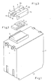
- FIG. 1 shows an electronic module 1, which is attached with its underside 2 on a top-hat rail, not shown.
- a socket 3 On the front side of the electronics module 1, a socket 3 is arranged for an erasable, programmable semiconductor read-only memory (EPROM) in a DIL housing 4.
- EPROM erasable, programmable semiconductor read-only memory
- DIL housing 4 At the top of the DIL housing there is a window 5 through which e.g. the memory content can be deleted with the help of UV light.
- Contact legs 6 which are bent downwards at right angles are arranged on the two long sides.
- a protective cap 7 made of opaque plastic can be snapped onto the DIL housing.
- the protective cap corresponds approximately to a cuboid, open box.
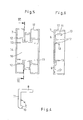
- the two end faces of the protective cap are provided with latching elements, which are designed as latching tongues 8, each with two slots 9 running from the end face to the center, and in each case by a free leg 11 adjoining it, running at right angles downward, with an inwardly bent latching nose 10 be formed. If the protective cap 7 is snapped onto the DIL housing 4, the detents 10 engage behind the DIL housing on its underside.
- a driver (not shown in the drawing) can be formed on the outer sides of the legs 11, approximately at the level of the latching lug 10.
- webs 12 are arranged on the inside of the base.
- the inner sides of the protective cap have projections 13 which protrude between the contact legs 6 for locking the DIL housing.
- the protective cap is provided on its upper side with a marking 18 for the correct insertion of the DIL housing 4 into the socket 3.
- the marking can be produced, for example, by a glued-on film or by screen printing.
Landscapes
- Semiconductor Memories (AREA)
- Casings For Electric Apparatus (AREA)
- Non-Volatile Memory (AREA)
- Emergency Protection Circuit Devices (AREA)
- Seal Device For Vehicle (AREA)
Abstract
Description
- Die Erfindung bezieht sich auf eine Schutzvorrichtung für einen integrierten Festkörperschaltkreis in einem DIL-Gehäuse, insbesondere für einen löschbaren, programmierbaren Halbleiterfestwertspeicher (EPROM) mit einem Fenster an der Oberseite des DIL-Gehäuses.
- Integrierte Festkörperschaltkreise sind sehr oft in einem DIL-Gehäuse (dual-in-line-Gehäuse) untergebracht. Die elektrischen Anschlüsse sind an den beiden Längsseiten hinter- 'einander angeordnet und meistens als Kontaktbeine rechtwinklig nach unten abgebogen. Die über das Gehäuse frei hinausragenden Kontaktbeine sind hierdurch für mechanische Beschädigungen relativ anfällig.
- Es sind Maßnahmen bekanntgeworden, DIL-Gehäuse mit ihren Kontaktbeinen in ein entsprechend zurechtgeschnittenes Stück Schaumstoff zu stecken, in dem sie für den Transport und bis zur endgültigen Montage verbleiben.
- Es ist weiterhin bekannt, gegen ungewolltes Löschen des Speicherinhalts durch Tages- bzw. künstliches Licht, die Fenster mit einem lichtundurchlässigen Klebestreifen zu - verschließen.
- Es hat sich gezeigt, daß die beiden vorgenannten Maßnahmen in ihrer Wirksamkeit ungenügend und von ihrer Anwendung her relatv umständlich sind.
- Der Erfindung liegt deshalb die Aufgabe zugrunde, mit einfachen Mitteln eine Schutzvorrichtung zu schaffen, welche einen mechanischen Schutz für die Kontaktbeine gewährleistet und einen ungewollten Lichteinfall durch das Fenster des DIL-Gehäuses verhindert.
- Diese Aufgabe wird erfindungsgemäß dadurch gelöst, daß auf. das DIL-Gehäuse eine Schutzkappe aufschnappbar ist mit die Kontaktbeine seitlich abdeckenden Seitenwänden, und daß das DIL-Gehäuse und die Schutzkappe eine Funktionseinheit bilden.
- Eine zweckmäßige Weiterbildung der Erfindung kann darin bestehen, daß die Schutzkappe an .ihren Stirnseiten jeweils ein Rastelement aufweist; welche das eingesetzte DIL-Gehäuse an der Unterseite hintergreifen, sowie darin, daß die Rastelemente als Rastzungen ausgebildet sind, durch jeweils von der Stirnseite der Schutzkappe zur Mitte hin verlaufende Schlitze, und daß der rechtwinklig nach unten verlaufende freie Schen- ,kel eine einwärtsgebogene Rastnase aufweist.
- Die mit der Erfindung erzielten Vorteile bestehen insbesondere darin, daß mit der Schutz- bzw. Deckkappe auf einfache Art und Weise die Kontaktbeine sicher gegen mechanische Beschädigung geschützt sind und gleichzeitig das Fenster lichtdicht verschlossen ist. Desweiteren bilden das DIL-Gehäuse und die Schutzkappe eine Funktionseinheit, d.h. die Schutzkappe verbleibt ständig auf dem DIL-Gehäuse und wird nur zum Löschen des Speicherinhalts abgezogen. Das DIL-Gehäuse kann also mit aufgeschnappter Schutzkappe in die Fassung gesteckt bzw. aus dieser wieder entfernt werden.
- Ein Ausführungsbeispiel der Erfindung ist in der Zeichnung dargestellt und wird im folgenden näher beschrieben.
- Es zeigen:
- Fig. 1 einen elektronischen Baustein mit einer an seiner Stirnseite angeordneten IC-Fassung;
- Fig. 2 einen integrierten Festkörperschaltkreis in einem DIL-Gehäuse;
- Fig. 3 eine Schutzkappe für das in Figur 2 gezeigte DIL-Gehäuse;
- Fig. 4 im Detail eine Rastzunge der in Figur 3 dargestellten Schutzkappe;
- Fig. 5 eine Ansicht von der Unterseite der Schutzkappe;
- Fig. 6 eine Ansicht im Schnitt in der Ebene VI - VI der Schutzkappe nach Fig. 5.
- Der Figur 1 ist ein elektronischer Baustein 1 zu entnehmen, der mit seiner Unterseite 2 auf einer nicht näher dargestellten Hutprofilschiene befestigt wird. An der Stirnseite des Elektronik-Bausteins 1 ist eine Fassung 3 angeordnet für einen löschbaren, programmierbaren Halbleiterfestwertspeicher (EPROM) in einem DIL-Gehäuse 4. An der Oberseite des DIL-Gehäuses befindet sich ein Fenster 5, durch welches z.B. mit Hilfe von UV-Licht der Speicherinhalt gelöscht werden kann. An den beiden Längsseiten sind rechtwinklig nach unten abgebogene Kontaktbeine 6 angeordnet. Auf das DIL-Gehäuse ist eine Schutzkappe 7 aus lichtundurchlässigem Plast aufschnappbar.
- Die Schutzkappe entspricht etwa einer quaderförmigen, offenen Schachtel. Die beiden Stirnseiten der Schutzkappe sind mit Rastelementen versehen, die als Rastzungen 8 ausgebildet sind durch jeweils zwei von der Stirnseite zur Mitte hin verlaufende Schlitze 9 sowie jeweils durch einen sich daran anschliessenden, rechtwinklig nach unten verlaufenden freien Schenkel 11, mit einer einwärtsgebogenen Rastnase-10 gebildet werden. Wird die Schutzkappe 7 auf das DIL-Gehäuse 4 aufgeschnappt, hintergreifen die Rastnasen 10 das DIL-Gehäuse an seiner Unterseite.
- Zum leichteren Lösen der Verrastung kann an den Außenseiten der SChenkel 11, etwa in Höhe der Rastnase 10, ein in der Zeichnung nicht näher dargestellter Mitnehmer angeformt sein.
- Durch den von dem freien Schenkel 11 und der Rastnase 10 gebildeten stumpfen Winkel (α) (Fig. 4) wird erreicht, daß die aufgeschnappte Schutzkappe 7 spielfrei auf dem DIL-Gehäuse 4 sitzt. Zur genauen Auflage des DIL-Gehäuses in der Schutzkappe sind auf der Bodeninnenseite Stege 12 angeordnet. Die Innenseiten der Schutzkappe weisen Anformungen 13 auf, welche zur Arretierung des DIL-Gehäuses zwischen die Kontaktbeine 6 ragen. Die Schutzkappe ist auf ihrer Oberseite mit einer Markierung 18 versehen zum seitenrichtigen Einsetzen äes DIL-Gehäuses 4 in die Fassung 3. Die Markierung kann beispielsweise durch eine aufgeklebte Folie, oder durch einen Siebdruck hergestellt werden.
Claims (8)
Priority Applications (1)
| Application Number | Priority Date | Filing Date | Title |
|---|---|---|---|
| AT80105239T ATE21974T1 (de) | 1979-09-11 | 1980-09-03 | Schutzkappe. |
Applications Claiming Priority (2)
| Application Number | Priority Date | Filing Date | Title |
|---|---|---|---|
| DE2936615 | 1979-09-11 | ||
| DE2936615A DE2936615C2 (de) | 1979-09-11 | 1979-09-11 | Schutzvorrichtung |
Publications (3)
| Publication Number | Publication Date |
|---|---|
| EP0025210A2 true EP0025210A2 (de) | 1981-03-18 |
| EP0025210A3 EP0025210A3 (en) | 1983-06-08 |
| EP0025210B1 EP0025210B1 (de) | 1986-09-03 |
Family
ID=6080525
Family Applications (1)
| Application Number | Title | Priority Date | Filing Date |
|---|---|---|---|
| EP80105239A Expired EP0025210B1 (de) | 1979-09-11 | 1980-09-03 | Schutzkappe |
Country Status (3)
| Country | Link |
|---|---|
| EP (1) | EP0025210B1 (de) |
| AT (1) | ATE21974T1 (de) |
| DE (1) | DE2936615C2 (de) |
Cited By (1)
| Publication number | Priority date | Publication date | Assignee | Title |
|---|---|---|---|---|
| WO2000001208A1 (en) * | 1998-06-30 | 2000-01-06 | Formfactor, Inc. | Assembly of an electronic component with spring packaging |
Family Cites Families (4)
| Publication number | Priority date | Publication date | Assignee | Title |
|---|---|---|---|---|
| US3548927A (en) * | 1968-11-29 | 1970-12-22 | Intern Electronic Research Co | Heat dissipating retainer for electronic component |
| US3684817A (en) * | 1971-03-04 | 1972-08-15 | Cogar Corp | Electronic module and cap therefor |
| DE7417008U (de) * | 1974-05-15 | 1974-09-12 | Cannon Electric Gmbh | Gehäuse zur Aufnahme eines integrierten Schaltungsbausteines |
| DE2633086B2 (de) * | 1975-08-01 | 1977-12-15 | Elektronisches programmierbares speicher-chip |
-
1979
- 1979-09-11 DE DE2936615A patent/DE2936615C2/de not_active Expired
-
1980
- 1980-09-03 AT AT80105239T patent/ATE21974T1/de not_active IP Right Cessation
- 1980-09-03 EP EP80105239A patent/EP0025210B1/de not_active Expired
Cited By (3)
| Publication number | Priority date | Publication date | Assignee | Title |
|---|---|---|---|---|
| US7202677B2 (en) | 1995-05-26 | 2007-04-10 | Formfactor, Inc. | Socket for mating with electronic component, particularly semiconductor device with spring packaging, for fixturing, testing, burning-in or operating such a component |
| US7534654B2 (en) | 1995-05-26 | 2009-05-19 | Formfactor, Inc. | Socket for making with electronic component, particularly semiconductor device with spring packaging, for fixturing, testing, burning-in or operating such a component |
| WO2000001208A1 (en) * | 1998-06-30 | 2000-01-06 | Formfactor, Inc. | Assembly of an electronic component with spring packaging |
Also Published As
| Publication number | Publication date |
|---|---|
| EP0025210B1 (de) | 1986-09-03 |
| DE2936615A1 (de) | 1981-03-26 |
| EP0025210A3 (en) | 1983-06-08 |
| ATE21974T1 (de) | 1986-09-15 |
| DE2936615C2 (de) | 1985-03-28 |
Similar Documents
| Publication | Publication Date | Title |
|---|---|---|
| DE29819517U1 (de) | Zugfederanschlußklemme | |
| EP0025210B1 (de) | Schutzkappe | |
| EP1093706A2 (de) | Gehäuse für eine elektronik-einheit, insbesondere für ein airbag-steuergerät | |
| WO1998047336A1 (de) | Elektrisches gerät mit zwei identisch aufgebauten gehäuseschalen | |
| DE3138042C2 (de) | Installationsgerät wie Leitungsschutzschalter oder Fehlerstromschutzschalter | |
| DE3874971T2 (de) | Anschlussmodul fuer elektrische leiter mit eingebauten bauteilen. | |
| EP1202582A2 (de) | Gehäuse für Telekommunikationsanlagen | |
| DE9418381U1 (de) | Einrichtung zum Erkennen einer Manipulation an einem geschlossenen Sicherungsgehäuse | |
| DE7600991U1 (de) | Gehäuse für eine einzelne Flachbaugruppe | |
| DE2748737A1 (de) | Belueftungsgitter | |
| DE2008512A1 (en) | Weatherproof housing for telecommunica-tion components | |
| DE4308242C1 (de) | Relais | |
| DE2923243C2 (de) | Gehäuse für elektrische Meßgeräte | |
| EP0617483A1 (de) | Kodierbarer Steckverbinder | |
| DE7909986U1 (de) | Elektrisches Schaltgerät mit Steckanschlüssen | |
| DE3050107T1 (de) | Arrangement for fitting a connection block in a cover | |
| DE8600635U1 (de) | Gehäuse für wassergeschützte Installationsgeräte | |
| DE3717019C2 (de) | Steckfassung für Flachstecker | |
| CH666567A5 (de) | Einteilige blechplombe. | |
| DE9318058U1 (de) | Gehäuse | |
| EP0617484A1 (de) | Kodierbarer Steckverbinder | |
| DE2846283A1 (de) | Blende fuer eine einschiebbare elektrische baugruppe | |
| CH683212A5 (de) | Elektronischer Festspeicher. | |
| DE19623615A1 (de) | Anordnung zur Sicherung eines steckbaren Elements in einem dafür vorgesehenen Gehäuse | |
| DE19604069A1 (de) | Batteriehaltevorrichtung |
Legal Events
| Date | Code | Title | Description |
|---|---|---|---|
| PUAI | Public reference made under article 153(3) epc to a published international application that has entered the european phase |
Free format text: ORIGINAL CODE: 0009012 |
|
| AK | Designated contracting states |
Designated state(s): AT BE CH FR GB IT NL SE |
|
| 17P | Request for examination filed |
Effective date: 19810427 |
|
| PUAL | Search report despatched |
Free format text: ORIGINAL CODE: 0009013 |
|
| AK | Designated contracting states |
Designated state(s): AT BE CH FR GB IT LI NL SE |
|
| GRAA | (expected) grant |
Free format text: ORIGINAL CODE: 0009210 |
|
| PGFP | Annual fee paid to national office [announced via postgrant information from national office to epo] |
Ref country code: AT Payment date: 19860812 Year of fee payment: 7 |
|
| AK | Designated contracting states |
Kind code of ref document: B1 Designated state(s): AT BE CH FR GB IT LI NL SE |
|
| REF | Corresponds to: |
Ref document number: 21974 Country of ref document: AT Date of ref document: 19860915 Kind code of ref document: T |
|
| ET | Fr: translation filed | ||
| ITF | It: translation for a ep patent filed | ||
| PLBE | No opposition filed within time limit |
Free format text: ORIGINAL CODE: 0009261 |
|
| STAA | Information on the status of an ep patent application or granted ep patent |
Free format text: STATUS: NO OPPOSITION FILED WITHIN TIME LIMIT |
|
| 26N | No opposition filed | ||
| PGFP | Annual fee paid to national office [announced via postgrant information from national office to epo] |
Ref country code: NL Payment date: 19870930 Year of fee payment: 8 |
|
| PG25 | Lapsed in a contracting state [announced via postgrant information from national office to epo] |
Ref country code: GB Effective date: 19880903 Ref country code: AT Effective date: 19880903 |
|
| PG25 | Lapsed in a contracting state [announced via postgrant information from national office to epo] |
Ref country code: SE Effective date: 19880904 |
|
| PG25 | Lapsed in a contracting state [announced via postgrant information from national office to epo] |
Ref country code: LI Effective date: 19880930 Ref country code: CH Effective date: 19880930 Ref country code: BE Effective date: 19880930 |
|
| BERE | Be: lapsed |
Owner name: BROWN BOVERI & CIE A.G. MANNHEIM Effective date: 19880930 |
|
| PG25 | Lapsed in a contracting state [announced via postgrant information from national office to epo] |
Ref country code: NL Effective date: 19890401 |
|
| NLV4 | Nl: lapsed or anulled due to non-payment of the annual fee | ||
| PG25 | Lapsed in a contracting state [announced via postgrant information from national office to epo] |
Ref country code: FR Free format text: LAPSE BECAUSE OF NON-PAYMENT OF DUE FEES Effective date: 19890531 |
|
| REG | Reference to a national code |
Ref country code: CH Ref legal event code: PL |
|
| GBPC | Gb: european patent ceased through non-payment of renewal fee | ||
| REG | Reference to a national code |
Ref country code: FR Ref legal event code: ST |
|
| EUG | Se: european patent has lapsed |
Ref document number: 80105239.0 Effective date: 19890614 |