EP0025647A2 - Elektrische Vorrichtung und Verfahren zum Fangen von Teilchen - Google Patents
Elektrische Vorrichtung und Verfahren zum Fangen von Teilchen Download PDFInfo
- Publication number
- EP0025647A2 EP0025647A2 EP80302876A EP80302876A EP0025647A2 EP 0025647 A2 EP0025647 A2 EP 0025647A2 EP 80302876 A EP80302876 A EP 80302876A EP 80302876 A EP80302876 A EP 80302876A EP 0025647 A2 EP0025647 A2 EP 0025647A2
- Authority
- EP
- European Patent Office
- Prior art keywords
- package
- organo polysiloxane
- particle
- particles
- electrical device
- Prior art date
- Legal status (The legal status is an assumption and is not a legal conclusion. Google has not performed a legal analysis and makes no representation as to the accuracy of the status listed.)
- Withdrawn
Links
Images
Classifications
-
- H—ELECTRICITY
- H10—SEMICONDUCTOR DEVICES; ELECTRIC SOLID-STATE DEVICES NOT OTHERWISE PROVIDED FOR
- H10W—GENERIC PACKAGES, INTERCONNECTIONS, CONNECTORS OR OTHER CONSTRUCTIONAL DETAILS OF DEVICES COVERED BY CLASS H10
- H10W76/00—Containers; Fillings or auxiliary members therefor; Seals
- H10W76/40—Fillings or auxiliary members in containers, e.g. centering rings
- H10W76/42—Fillings
- H10W76/48—Fillings including materials for absorbing or reacting with moisture or other undesired substances
-
- H—ELECTRICITY
- H10—SEMICONDUCTOR DEVICES; ELECTRIC SOLID-STATE DEVICES NOT OTHERWISE PROVIDED FOR
- H10W—GENERIC PACKAGES, INTERCONNECTIONS, CONNECTORS OR OTHER CONSTRUCTIONAL DETAILS OF DEVICES COVERED BY CLASS H10
- H10W76/00—Containers; Fillings or auxiliary members therefor; Seals
- H10W76/10—Containers or parts thereof
- H10W76/12—Containers or parts thereof characterised by their shape
- H10W76/13—Containers comprising a conductive base serving as an interconnection
- H10W76/132—Containers comprising a conductive base serving as an interconnection having other interconnections through an insulated passage in the conductive base
-
- H—ELECTRICITY
- H10—SEMICONDUCTOR DEVICES; ELECTRIC SOLID-STATE DEVICES NOT OTHERWISE PROVIDED FOR
- H10W—GENERIC PACKAGES, INTERCONNECTIONS, CONNECTORS OR OTHER CONSTRUCTIONAL DETAILS OF DEVICES COVERED BY CLASS H10
- H10W90/00—Package configurations
- H10W90/701—Package configurations characterised by the relative positions of pads or connectors relative to package parts
- H10W90/751—Package configurations characterised by the relative positions of pads or connectors relative to package parts of bond wires
- H10W90/754—Package configurations characterised by the relative positions of pads or connectors relative to package parts of bond wires between a chip and a stacked insulating package substrate, interposer or RDL
Definitions
- This invention relates to the manufacture of electrical devices and more particularly to an improved electrical device.
- electrical devices comprise electrical components such as semiconductors, resistors (thick and thin film), hybrid microcircuit devices and the like are disposed within the interior of a protective package or housing, and the interior of the package is normally provided with a suitable inert atmosphere.
- the package conventionally comprises a base portion and a lid portion, with the functioning electrical components being carried on the base portion and the lid being permanently fastened onto the base by suitable sealing methods such as welding, soldering or adhesives such as epoxy resins and the like.
- PIND particle impact noise detection
- a variety of methods have been proposed and utilized to alleviate the particle problem in devices utilizing sealed packages. For example, great care has been utilized in the processing itself to avoid the production of particles and to reduce the possibility of such particles being in the atmosphere at the time of sealing the package of the device. In certain cases a small resealable opening is provided in the package for removal of particles after manufacture of the electrical device. After removing the particles the opening in the package is resealed. Needless to say, the foregoing methods require extreme care during the manufacturing operations and, in many cases, are ineffective in the prevention of particles within the package of the electrical device. ,
- the present invention overcomes the foregoing deficiencies in sealed package electrical devices with respect to foreign particles.
- a polysiloxane elastomeric "particle getter” material in a partially cured condition is introduced into the package of an electrical device manufactured in accordance with the present invention.
- the particle getter material serves to entrap and retain foreign particles which- may be contained in the package.
- the particle getter material is partially cured to a substantially nonflowing condition so that it remains in position within the package remote from the functioning electrical component or components of the device and so that it does not interfere with any of the manufacturing operations, particularly the sealing operation.
- the partially cured particle getter material is operative over a wide temperature range to entrap and retain foreign particles.
- the particle getter material may function as an adhesive trap to hold particles on the surface of the particle getter.
- the particle getter may also function to entrap particles within the body of the material or the particle getter may function by some other entrappingmechanism.
- the present invention is applied to a wide variety of electrical devices which include a sealed package for protection of the functioning electrical components.
- the present invention may be utilized in connection with the manufacture of semiconductors, hybrid microcircuits, relays, thin film and thick film resistors, and other similar electrical devices in which the functioning electrical component is disposed in a package or container for protection.
- the polysiloxane particle getter material may be selected from a wide variety of organo polysiloxanes which are commercially available.
- the base resin may comprise polysiloxanes such as dimethyl siloxane, diphenyl siloxane, methyl phenyl siloxane, phenyl vinyl siloxane, tetraethoxy siloxane and the like,- and may further include groups such as vinyl groups which aid in the cross linking and curing of the polysiloxane.
- Organo polysiloxanes often include mixtures of random organo polysiloxanes and block organo polysiloxanes.
- the polysiloxane material may include various additives such as quartz, silica, diatomaceous earth and pigments.
- the polysiloxane getter material must be capable of operation within an enclosed environment and thus must not during curing or during the useful life of the device, give off any byproducts which would be harmful to the active component of the electrical device. Accordingly, the polysiloxane must be inert with respect to the elements of the electric device and to its function.
- the composition of the particle getter must also be capable of capturing and retaining foreign particles within the electrical device over a wide range of temperatures. In the present invention it is preferred that the particle getter composition be operative at temperatures ranging from -65°C to 150°C. Polysiloxanes being relatively heat insensitive have this property when partially cured in accordance with the present invention. In addition to being operable over a wide range of temperatures, it is also highly preferred that the polysiloxane composition retain its particle capturing and retaining properties over a long period of time, at least during the useful life of the electrical device.
- the polysiloxane particle getter composition is partially cured to a nonflowing condition and in this partially cured condition meets the criteria set forth above for the particle getter composition of the present invention.
- partial cure refers to the fact that less than the recommended or theoretical quantity of curing agent is added to the resin to effect the cross-linking thereof and does not refer to curing times or temperatures.
- a precise ratio of parts of resin to parts of curing agent or percentage of curing agent in the total composition cannot be provided.
- the particle getter composition in the uncured state must contain at least a sufficient amount of curing agent to provide a finished elastomer composition which is substantially nonflowing in the package of the finished electrical device and which is capable of entrapping and retaining particles but less than that amount of curing agent to complete the cure or cross linking the organo polysiloxane.
- the organo polysiloxane composition contains less than about 9 parts by weight of curing agent per 100 parts by weight of polysiloxane base resin.
- the polysiloxane functions well to entrap and retain particles throughout a broad range of proportion of curing agent to base resin, it has been found that the uncured polysiloxane is easiest to work with when the curing agent comprises between about 2 parts and about 4 parts per 100 parts of base resin.
- organo polysiloxane resins are organic peroxides such as, for example, 2,5-bis(tertiary-butyl peroxy)-2,5-dimethyl hexane and dicumyl peroxide, tert-butyl peroxybenzoate, or benzoyl peroxide; quartenary ammonium salts of strong acids; and alcoholic solutions of platinum such as, for example, a solution of chloroplatinic acid in 2-ethyl hexanol.
- organic peroxides such as, for example, 2,5-bis(tertiary-butyl peroxy)-2,5-dimethyl hexane and dicumyl peroxide, tert-butyl peroxybenzoate, or benzoyl peroxide
- quartenary ammonium salts of strong acids such as, for example, a solution of chloroplatinic acid in 2-ethyl hexanol.
- the organo polysiloxane material is introduced during manufacture of the device into a package, preferably at a spot within the package which is remote from the operational element or elements of the electrical device.
- the particle getter material which comprises the reaction product of a mixture of the organo polysiloxane and curing agent is generally in the fully uncured, free flowing condition when placed in the package. Accordingly, the package and getter material are normally subjected to elevated curing temperatures for a sufficient period of time to effect the in situ partial curing of the organo polysiloxane material to render the material substantially nonflowing.
- This curing step which serves also to secure the organo polysiloxane within the package, may be carried out before or after sealing the package.
- the getter material may be cured prior to its introduction into the package. In such a case, however, normally an additional bonding agent suitable for use within the package will be required to secure the getter material in its place within the package.
- the package is then sealed and subsequently agitated, thereby to cause foreign particles which may be within the package to become mobilized, entrapped and retained in the organo polysiloxane particle getter material.
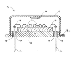
- the figure is a cross sectional view showing an electrical device incorporating particle getter material in accordance with the present invention.
- the electrical device comprises a package, shown generally as 10, comprising a base or header 11 provided with openings 12 for the extension therethrough of terminal pins 13.
- the terminal pins 13 are sealed into the openings 12 by glass seals 14.
- the package is completed by a lid 15 which is provided with an outwardly flaring lip 15a for sealing on the header.
- the operational element of the electrical device comprises a substrate 16 which is affixed to the inner surface of the header 11.
- the header 11 carries an integrated circuit 17 prepared in accordance with standard methods well understood in the art. Wire bonds 18 interconnect the various portions of the integrated circuit 17 and the terminal pins 13.
- an organo polysiloxane material (19) is disposed on the inner surface of the lid 15 substantially directly over the integrated circuit 17.
- the organo polysiloxane material (19) is partially cured so that it is substantially nonflowing and thus maintains its position on the underside of the lid 15 and does not creep or flow down on to the integrated circuit or the sealing area between the header and the outwardly flared lip 15a. It is preferred in manufacturing electrical devices in accordance with the present invention to invert the lid and place the drop of particle getter material (19) on the inner surface of the lid.
- the lid is then subjected to an elevated temperature for sufficient time to complete the partial cure of the organo polysiloxane material.
- the time and temperature will depend to some extent upon the nature of the organo polysiloxane, the curing agent and the amount of curing agent contained in the uncured mix.
- the polysiloxane material is sufficiently nonflowing to maintain its position when the'lid is inverted into its normal position on the header.
- Sealing may be accomplished by welding, soldering or by the use of suitable adhesive material such as the epoxy adhesives.
- sealing is carried out in an inert atmosphere after an appropriate vacuum bake.
- the package may be evacuated after sealing by providing a resealable opening in the header 11 or the lid 15 and if desired, an inert atmosphere can be introduced into the package 10 prior to resealing.
- the following example demonstrates the effectiveness of an organo polysiloxane particle getter composition containing varying amounts of curing agent.
- Samples were prepared which consisted of a ceramic substrate on which an area 0.2 by 0.4 inches was marked out in approximately the center of the substrate. The marked out area was to receive the particle getter composition.
- the particle getter composition comprised a methyl phenyl siloxane base resin and a platinum curing agent manufactured by Dow Corning and sold under the trademark "SYLGARD '184". Sixteen particle getter compositions were prepared from the base polysiloxane resin and varying amounts of curing agent. The compositions were prepared in accordance with the following schedule:
- test devices were prepared for each of the particle getter compositions by placing a sufficient amount of the particle getter composition to provide a substantially uniform coating to cover the marked out area of the ceramic base (about 8 mg).
- the bases were subjected to heating at 150°C for one half hour to cure the particle getter composition followed by a vacuum bake at 150°C for sixteen hours.
- each of the lids was placed two solder balls (3-10 mil diameter), one piece of aluminum approximately 5 mil diameter by 5 mil long and one piece of gold bond wire, 1 mil diameter by 10-20 mils long to simulate typical deleterious particles which could be found in sealed electrical devices.
- the devices were assembled, keeping the lids upside down in order to maintain the particles in place and using epoxy as the sealing agent.
- the units were cured for an additional two hours at approximately 170°C in order to complete the hardening of the epoxy.
- the units were tested for particles using MIL-Std-883, Method 2020 Condition A. This basically comprised subjecting the unit to shock and vibration to determine whether the unit initially contained loose particles, followed by three additional cycles of shock end vibration to determine the amount of time required to trap the particles and to see if the getter material retained the particles.
- the particles are sensed by attaching the unit being tested to an acoustical transducer and displaying the transducer output. Following the first cycle, the units were subjected to one half hour at 100°C storage to reduce any static locking of the particles. All of the units were then re-tested as set out above.
- the getter composition containing from about 1 to about 9 parts of curing agent per 100 parts of resin exhibited the ability to capture particles and not flow outside of the marked off area of the ceramic base.
- Getter compositions containing in excess of about 9 parts of curing agent per 100 parts of resin is not as effective in capturing particles.
- the composition containing no curing agent was considered undesirable in that it flowed beyond the marked off area and, in fact, covered the entire inner surface of the test device.
- Additional tests were run on devices manufactured as in this Example I, however using soldered joints. The results indicated that the presence of the getter material did not adversely affect the solder joint or materially increase the number of leaking devices over statistical norms for conventionally manufactured devices. The performance of getter material was not adversely affected by the soldering operation.
- Test devices were prepared as in Example I using three and one half parts of the curing agent per 100 parts of the polysiloxane composition of Example I. After curing and baking, the units were sealed with epoxy resin as in Example I and tested for initial particles. All units were free of loose particles at the end of the first particle test cycle. The units were then subjected to temperatures of -65°C for at least 48 hours. The units were then re-tested for the presence of particles while still cold. Out of twenty units one unit exhibited the presence of free particles during the first test cycle but exhibited no evidence of loose particles by the fourth test cycle and remained so for three additional test cycles. The remaining nineteen units tested free of loose particles after the first cycle and remained so after three additional test cycles.
Landscapes
- Structures Or Materials For Encapsulating Or Coating Semiconductor Devices Or Solid State Devices (AREA)
- Compositions Of Macromolecular Compounds (AREA)
- Casings For Electric Apparatus (AREA)
Applications Claiming Priority (2)
| Application Number | Priority Date | Filing Date | Title |
|---|---|---|---|
| US75864 | 1979-09-17 | ||
| US06/075,864 US4352119A (en) | 1979-09-17 | 1979-09-17 | Electrical device and method for particle entrapment device for an electrical component |
Publications (2)
| Publication Number | Publication Date |
|---|---|
| EP0025647A2 true EP0025647A2 (de) | 1981-03-25 |
| EP0025647A3 EP0025647A3 (de) | 1983-03-30 |
Family
ID=22128465
Family Applications (1)
| Application Number | Title | Priority Date | Filing Date |
|---|---|---|---|
| EP80302876A Withdrawn EP0025647A3 (de) | 1979-09-17 | 1980-08-20 | Elektrische Vorrichtung und Verfahren zum Fangen von Teilchen |
Country Status (2)
| Country | Link |
|---|---|
| US (1) | US4352119A (de) |
| EP (1) | EP0025647A3 (de) |
Cited By (6)
| Publication number | Priority date | Publication date | Assignee | Title |
|---|---|---|---|---|
| FR2538618A1 (fr) * | 1982-12-28 | 1984-06-29 | Inf Milit Spatiale Aeronaut | Boitier pour composant electronique comportant un element fixant l'humidite |
| EP0707360A1 (de) * | 1994-10-11 | 1996-04-17 | Corning Incorporated | Lasergehäuse mit Veruntreinigungs Getter |
| US5629952A (en) * | 1993-07-14 | 1997-05-13 | Corning Incorporated | Packaging of high power semiconductor lasers |
| WO2006057940A1 (en) * | 2004-11-24 | 2006-06-01 | Northrop Grumman Corporation | Integrated multi-purpose getter for radio-frequency (rf) circuit modules |
| DE102010019027A1 (de) | 2010-05-03 | 2011-11-03 | Audi Ag | Einrichtung zum Aufnehmen von Hydraulikfluid für ein Getriebe eines Kraftwagens sowie Bauteil hierfür |
| US11787097B2 (en) | 2021-02-10 | 2023-10-17 | Nxp Usa, Inc. | Conduit inserts for encapsulant compound formulation kneading and encapsulation back-end assembly processes |
Families Citing this family (12)
| Publication number | Priority date | Publication date | Assignee | Title |
|---|---|---|---|---|
| US4622433A (en) * | 1984-03-30 | 1986-11-11 | Diacon, Inc. | Ceramic package system using low temperature sealing glasses |
| US4868639A (en) * | 1986-08-11 | 1989-09-19 | Fujitsu Limited | Semiconductor device having waveguide-coaxial line transformation structure |
| US5196919A (en) * | 1990-12-07 | 1993-03-23 | Kyocera America, Inc. | Use of a contamination shield during the manufacture of semiconductor packages |
| US5734226A (en) * | 1992-08-12 | 1998-03-31 | Micron Technology, Inc. | Wire-bonded getters useful in evacuated displays |
| US5939785A (en) * | 1996-04-12 | 1999-08-17 | Texas Instruments Incorporated | Micromechanical device including time-release passivant |
| DE19734032C1 (de) * | 1997-08-06 | 1998-12-17 | Siemens Ag | Elektronisches Steuergerät mit Kontaktstift sowie Herstellungsverfahren |
| US5929515A (en) * | 1997-10-01 | 1999-07-27 | The Charles Stark Draper Laboratory, Inc. | Gettering enclosure for a semiconductor device |
| AU2502300A (en) * | 1999-01-12 | 2000-08-01 | Teledyne Technologies Incorporated | Micromachined device and method of forming the micromachined device |
| US7091605B2 (en) * | 2001-09-21 | 2006-08-15 | Eastman Kodak Company | Highly moisture-sensitive electronic device element and method for fabrication |
| KR100883075B1 (ko) * | 2007-03-02 | 2009-02-10 | 엘지전자 주식회사 | 전계발광소자 |
| DE102011056742B4 (de) * | 2011-05-09 | 2019-07-18 | Conti Temic Microelectronic Gmbh | Steuergerät mit einer Getterschicht in einem Kraftfahrzeug |
| GR1007811B (el) | 2011-09-30 | 2013-01-25 | Ιωαννης Σταυρου Ιωαννιδης | Συναρμολογουμενη ανεμογεννητρια με ειδικους βραχιονες φεροντες αναδιπλουμενα πτερυγια και μηχανισμο φρενου για τη ρυθμιση των περιστροφων των βραχιονων |
Family Cites Families (14)
| Publication number | Priority date | Publication date | Assignee | Title |
|---|---|---|---|---|
| US2928030A (en) * | 1954-06-07 | 1960-03-08 | Itt | Semiconductor devices |
| BE516590A (de) * | 1951-10-29 | |||
| US2988676A (en) * | 1957-07-15 | 1961-06-13 | Pacific Semiconductors Inc | Semiconductor device |
| US2987799A (en) * | 1957-07-15 | 1961-06-13 | Pacific Semiconductors Inc | Mobile particle entrapment method |
| US3056074A (en) * | 1960-11-03 | 1962-09-25 | Philco Corp | Miniature desiccator and production of units thereof |
| US3259490A (en) * | 1963-05-07 | 1966-07-05 | Motorola Inc | Gettering in semiconductor devices |
| GB1104117A (en) * | 1964-12-04 | 1968-02-21 | Dow Corning | Organosilicon compositions |
| GB1137286A (en) * | 1965-09-07 | 1968-12-18 | Texas Instruments Inc | Protective element for hermetically enclosed semiconductor devices |
| US3398551A (en) * | 1966-10-03 | 1968-08-27 | Carrier Corp | Compressor control including pressure equalizer and overpressure means |
| DE1926575A1 (de) * | 1969-05-23 | 1970-11-26 | Wacker Chemie Gmbh | Verfahren zum Umhuellen von elektrischen und elektronischen Bauteilen |
| US4042955A (en) * | 1973-06-22 | 1977-08-16 | Nippondenso Co., Ltd. | Resin-sealed electrical device |
| US3844992A (en) * | 1973-11-16 | 1974-10-29 | Dow Corning | Wood graining tool fast cure organopolysiloxane resins |
| US4017340A (en) * | 1975-08-04 | 1977-04-12 | General Electric Company | Semiconductor element having a polymeric protective coating and glass coating overlay |
| US4096521A (en) * | 1976-07-08 | 1978-06-20 | Motorola Inc. | Protective coating for high voltage devices |
-
1979
- 1979-09-17 US US06/075,864 patent/US4352119A/en not_active Expired - Lifetime
-
1980
- 1980-08-20 EP EP80302876A patent/EP0025647A3/de not_active Withdrawn
Cited By (12)
| Publication number | Priority date | Publication date | Assignee | Title |
|---|---|---|---|---|
| FR2538618A1 (fr) * | 1982-12-28 | 1984-06-29 | Inf Milit Spatiale Aeronaut | Boitier pour composant electronique comportant un element fixant l'humidite |
| EP0113282A1 (de) * | 1982-12-28 | 1984-07-11 | Thomson-Csf | Gehäuse für einen elektronischen Baustein mit einem feuchtigkeitsfixierenden Element |
| US4553020A (en) * | 1982-12-28 | 1985-11-12 | Compagnie D'informatique Militaire, Spatiale Et Aeronautique | Electronic component package comprising a moisture-retention element |
| US5629952A (en) * | 1993-07-14 | 1997-05-13 | Corning Incorporated | Packaging of high power semiconductor lasers |
| US5770473A (en) * | 1993-07-14 | 1998-06-23 | Corning Incorporated | Packaging of high power semiconductor lasers |
| EP0707360A1 (de) * | 1994-10-11 | 1996-04-17 | Corning Incorporated | Lasergehäuse mit Veruntreinigungs Getter |
| WO2006057940A1 (en) * | 2004-11-24 | 2006-06-01 | Northrop Grumman Corporation | Integrated multi-purpose getter for radio-frequency (rf) circuit modules |
| US7315069B2 (en) | 2004-11-24 | 2008-01-01 | Northrop Grumman Corporation | Integrated multi-purpose getter for radio-frequency (RF) circuit modules |
| DE102010019027A1 (de) | 2010-05-03 | 2011-11-03 | Audi Ag | Einrichtung zum Aufnehmen von Hydraulikfluid für ein Getriebe eines Kraftwagens sowie Bauteil hierfür |
| DE102010019027B4 (de) * | 2010-05-03 | 2021-06-17 | Audi Ag | Bauteil für eine Einrichtung zum Aufnehmen von Hydraulikfluid für ein Getriebe eines Kraftwagens |
| US11787097B2 (en) | 2021-02-10 | 2023-10-17 | Nxp Usa, Inc. | Conduit inserts for encapsulant compound formulation kneading and encapsulation back-end assembly processes |
| US12415305B2 (en) | 2021-02-10 | 2025-09-16 | Nxp Usa, Inc. | Conduit inserts for encapsulant compound formulation kneading and encapsulation back-end assembly processes |
Also Published As
| Publication number | Publication date |
|---|---|
| EP0025647A3 (de) | 1983-03-30 |
| US4352119A (en) | 1982-09-28 |
Similar Documents
| Publication | Publication Date | Title |
|---|---|---|
| US4382327A (en) | Method for particle entrapment within an electrical device package | |
| US4352119A (en) | Electrical device and method for particle entrapment device for an electrical component | |
| US4081397A (en) | Desiccant for electrical and electronic devices | |
| US6770968B2 (en) | Method for bonding heat sinks to overmolds and device formed thereby | |
| US4521469A (en) | Casing for electronic components | |
| US5165956A (en) | Method of encapsulating an electronic device with a silicone encapsulant | |
| EP0803542A3 (de) | Elektrisch leitfähige Silikonkautschukzusammensetzung und ihre Anwendung zur Herstellung von Halbleiteranordnungen | |
| JPS646538B2 (de) | ||
| JP3760063B2 (ja) | 接着剤と封入剤の同時硬化によるエレクトロニックパッケージの製造方法 | |
| CA1246757A (en) | Magnetically sealed multichip integrated circuit package | |
| JPS5987840A (ja) | 半導体装置 | |
| JPH08316357A (ja) | 樹脂封止型パワーモジュール装置 | |
| US4355719A (en) | Mechanical shock and impact resistant ceramic semiconductor package and method of making the same | |
| US5946554A (en) | Method of producing resin-sealed electronic device | |
| US6560839B1 (en) | Method for using a moisture-protective container | |
| JPH0864759A (ja) | 樹脂封止型パワーモジュール装置及びその製法 | |
| JPH1050775A (ja) | 半導体装置用両面接着絶縁テープ及びこれを用いたリードフレーム | |
| US4552267A (en) | Ceramic semiconductor package chip prevention structure and method | |
| US5597610A (en) | Method for coating electric component with resin | |
| JP3070929B2 (ja) | パッケージの組立方法とパッケージ | |
| KR0168841B1 (ko) | 금속전자 패키지 및 그 제조공정 | |
| JPS6351660A (ja) | 電子回路デバイスとその製造方法 | |
| Martin et al. | Humidity test of premolded chip carriers | |
| JPH0936066A (ja) | 半導体ウエハ固定用粘着テープ | |
| KR880001538B1 (ko) | 아이시(ic)칩 보호 코팅방법 |
Legal Events
| Date | Code | Title | Description |
|---|---|---|---|
| PUAI | Public reference made under article 153(3) epc to a published international application that has entered the european phase |
Free format text: ORIGINAL CODE: 0009012 |
|
| AK | Designated contracting states |
Designated state(s): DE FR GB NL |
|
| 17P | Request for examination filed |
Effective date: 19810908 |
|
| PUAL | Search report despatched |
Free format text: ORIGINAL CODE: 0009013 |
|
| AK | Designated contracting states |
Designated state(s): DE FR GB NL |
|
| STAA | Information on the status of an ep patent application or granted ep patent |
Free format text: STATUS: THE APPLICATION HAS BEEN WITHDRAWN |
|
| 18W | Application withdrawn |
Withdrawal date: 19851028 |
|
| RIN1 | Information on inventor provided before grant (corrected) |
Inventor name: NELSON, GALE CHARLES Inventor name: BARDENS, WILLIAM HENRY |