EP0025672A1 - Apparat zur Umsetzung von Bildabtastsignalen in Halbtonbildsignale - Google Patents
Apparat zur Umsetzung von Bildabtastsignalen in Halbtonbildsignale Download PDFInfo
- Publication number
- EP0025672A1 EP0025672A1 EP19800303096 EP80303096A EP0025672A1 EP 0025672 A1 EP0025672 A1 EP 0025672A1 EP 19800303096 EP19800303096 EP 19800303096 EP 80303096 A EP80303096 A EP 80303096A EP 0025672 A1 EP0025672 A1 EP 0025672A1
- Authority
- EP
- European Patent Office
- Prior art keywords
- memory
- output
- words
- comparator
- halftone
- Prior art date
- Legal status (The legal status is an assumption and is not a legal conclusion. Google has not performed a legal analysis and makes no representation as to the accuracy of the status listed.)
- Withdrawn
Links
- 238000013507 mapping Methods 0.000 title claims 3
- 230000015654 memory Effects 0.000 claims abstract description 20
- 238000006243 chemical reaction Methods 0.000 claims abstract description 11
- 239000011159 matrix material Substances 0.000 claims description 23
- 230000001419 dependent effect Effects 0.000 claims 1
- 230000005540 biological transmission Effects 0.000 description 6
- 238000000034 method Methods 0.000 description 6
- 230000006870 function Effects 0.000 description 3
- 230000008878 coupling Effects 0.000 description 1
- 238000010168 coupling process Methods 0.000 description 1
- 238000005859 coupling reaction Methods 0.000 description 1
- 238000005070 sampling Methods 0.000 description 1
Images



Classifications
-
- H—ELECTRICITY
- H04—ELECTRIC COMMUNICATION TECHNIQUE
- H04N—PICTORIAL COMMUNICATION, e.g. TELEVISION
- H04N1/00—Scanning, transmission or reproduction of documents or the like, e.g. facsimile transmission; Details thereof
- H04N1/40—Picture signal circuits
- H04N1/405—Halftoning, i.e. converting the picture signal of a continuous-tone original into a corresponding signal showing only two levels
- H04N1/4055—Halftoning, i.e. converting the picture signal of a continuous-tone original into a corresponding signal showing only two levels producing a clustered dots or a size modulated halftone pattern
Definitions
- the image is one of black print on a white background. This information is easily transmitted in binary digits and reproduced as black and white areas.
- a second consideration is that in the reproduction of the image on paper, the common office copies and facsimile equipment cannot print gray scale directly.
- the image must first be reduced to a halftone image, comprising a matrix of black and white bits. Shades of gray are then reproduced by varying the relative size of the dots.
- a matrix of pixels, eight pixels on a side would be used to create two black and two white dots.
- a halftone system using one bit per pixel would be advantageous.
- One efficient method of handling gray scale information is to use a continuous analog voltage which is representative of one line of the image, and to convert that continuous analog voltage into a one-bit per pixel halftone bit map before transmission storage or reproduction. Since high raster input scanner rates have become common, it is also necessary that the circuit which accomplishes this halftone conversion must be capable of operating at high data rates.
- a further complication is that the matrix values for each matrix position are different, and must be changed from one pixel to the next and from one row to the next.
- the first three positions in the first row of the matrix have threshold levels of 12,10, and 8 in a scale of from 0 to 63, and the first three positions in the second row are 14, 0, and 6.
- the circuit must be able, first, to compare the instant analog input voltage to each new threshold level in the row, and second, to supply a new set of values for each new row, all at practical data rates..
- the characteristics of the original image, the raster input scanner and the output marking engine may be compensated for by varying the matrix threshold values.
- a circuit with a provision for conveniently modifying the matrix values would be useful.
- a higher speed version comprises eight channels operating concurrently to produce the halftone bit maps. Since there are eight pixels per matrix, each channel is loaded with its threshold level at the beginning of the scan and uses that value for the duration of the scan. Between scan lines, the threshold values are changed, but this is accomplished during a short quiescent interval so the data rate is not affected.
- Each channel comprises a digital to analog converter to produce a threshold or reference voltage which is compared with the input voltage or pixel at a comparator to generate one binary digit.
- the eight bit converter input is supplied from the memory of a resident processor or equivalent so that the matrix valuesmaybe varied in real time to satisfy varying conditions if required.
- a lower cost alternative circuit is also described.
- the part count is minimized by using a single channel, but the data rate is maintained at a high level through the use of high speed components in the critical portions of the circuit.
- the threshold voltages are generated from digital signals output from RAM devices which are reprogrammable between documents.
- the object of this invention is to provide a circuit which can accomplish the high speed conversion of an analog voltage to a one bit per pixel halftone bit map, and l wwch can.'vary the matrix values in real time to compensate for variable system characteristics.
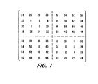
- Fig. 1 is an example of a 64 element matrix used in halftone conversion.
- Each threshold voltage level corresponds to one of 64 points on a scale from white to black. At every sampling point, if the value of the image pixel is larger than the specified threshold value at that point, the output image will appear as a binary white. Otherwise, it will appear black.
- the elements are arranged in a double spiral pattern which, for gray shades, results in two white and two black dots, the white dots comprising the upper left and lower right quarters. These dots are "grown" so that, for instance, a light shade of gray will be reproduced as a mainly white matrix with small black dots centered in the upper right and lower left quarters.
- the resultant halftone image shows a diagonal pattern which may be more pleasing to the eye than a vertical/horizontal pattern.
- Fig. 2 is the schematic of one of eight channels of the halftone conversion circuit.
- the digital-to-analog converter 10 receives an eight bit digital input and a five volt reference voltage, shown connected to pin 14, and produces an analog reference voltage at pin 4. .
- a latched comparator 11 compares the analog image input voltage with this reference and produces a binary output which is a one bit pixel of halftone information.
- the digital inputs and voltage output of the converter 10 need not be changed for the duration of the line-scan.
- the values are updated between scans, but the quiescent time is greater than the converter 10 setting time.
- the timing for this process is controlled by the mod 8 counter 13 and a decoder 14 which control each comparator 11 through an associated gate 15. Since the analog input voltage is continuously applied to all comparators 11, the mod 8 counter simultaneously selects . one comparator 11 through the decoder 14 and the individual channel's gate 15, and selects the associated multiplexer 12 input to enable each channel output.
- the eight sets of eight bit inputs applied to the converters 10 are applied by the circuit of Fig. 3 which is an interface circuit between a processor which supplies the matrix values and the converters 10 of Fig. 2.
- Each set of eight bit threshold values is supplied to each converter by a pair of memory devices 20, 21 on lines ND00 through ND07. This information is first received from the controlling computer lines on DATA 0 through DATA 7, and is distributed through drives 22 through 29 to the eight sets of memory devices in parallel.
- the particular memory device to be loaded is identified by the controller by the bit pattern of lines DATA 13 14, and 15, which is latched into device 30 and decoded in decoder 31 to drive one of eight enable lines WEO through WE7.
- a clock is received from the controller at the end of each scan on line IOPLS and is coupled through gates 33 and 34 to drive the counter 32.
- the board is given an address by using a set of switches 35 to establish a bit pattern on lines ADO through AD5. If the computer calls the board by setting lines DSO through DS5 to the same pattern, then digital comparator 36 will output a signal to allow the clock pulse IOPLS to be coupled through gate 33 to the 8 counter 32.
- a multiplexer 37 is included in each channel.
- latch 30 controls the multiplexer 37 to select one memory output line, the state of which is coupled through gate 38 to the controller to verify the proper operation of the circuit.
- the memory devices 20, 21 are each loaded with eight words when the system is first turned on, and will, thereafter, cycle through these eight words repetitively as each row of each matrix is needed.
- a new set of matrix values may be required. This could be accomplished by another loading operation. This, of course, would require a significant amount of loading time and would be done between documents to be scanned.
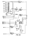
- FIG. 4 An alternative circuit for generating a series of eight-bit outputs for the converter of Fig. 2 is shown in Fig. 4.
- the RAM of Fig. 4 produces one digital threshold value at a time.
- This is, therefore, a single channel circuit instead of a circuit with eight channels in parallel but the data rate is half that of the Fig. 2, Fig. 3 equivalent because of the use of faster components, particularly a faster digital-to-analog converter which, however, is less accurate ( 6 bits compared to 8 bits in the circuit of Fig. 2, Fig. 3).
- Suitable parts for this application are the Signetcis NE5008 and the Analog Devices DAC-08.
- Fig. 4 two 256x4 bit RAMs 40,41 supply an eight bit output HTDO through HTD7, of which only HDTO throught HDT5 are used. Data to be loaded into these RAMs 40, 41aresupplied by the Microprocessor Unit (MPU) data bus which is connected directly to the device input pins via lines DO through D7. Again, only the first six lines are used in this embodiment.
- MPU Microprocessor Unit
- Each RAM 40, 41 receives six bits of addressing information at pins AO through A5 from multiplexer 42,43.
- the alternate sources of addressing are the MPU address bus which supplies a six bit address on lines AO through A5, and an eight line counter 44, 45 which supplies a six bit address to the multiplexer 42, 43 at pins A1, A2, A3 and A4 multiplexer of 42 and at pins A3 and A4 of mulitplexer 43.
- the mod-8 pixel counter 45 accomplishes this function by supplying the least significant three bits of addressing information to the multiplexers 42, 43 and RAMs 40, 41.
- the matrix, and therefore the RAMs 40, 41 must be switched to the next set of eight values. This is done by incrementing the mod-8 line counter 44 at the end of each line, thereby incrementing the most significant three bits of the RAM 40,41 address.
- the remainder of the circuitry is random logic which allows the circuit to be controlled by an MPU to perform its various subsidiary functions.
- the SI input to the multiplexers is used during the RAM loading process to select addressing data from the MPU at the same time that data is presented to the RAMs by the MPU data bus.
- the RAMs 40, 41 must be write-enabled.
- the board is supplied with an address decoder 47 to perform the function of switches 35 and-comparator 36 of Fig. 3.
- decoder 47 of Fig. 4 When the board address is received at decoder 47 of Fig. 4, it supplies an enabling pulse to decoder 48.
- This decoder simultaneously receives MPU address bus, A0, Al, A2, - to generate an Sl, S2,or S3 output.
- the S3 output is used to reset the counters 44 and 45, and the S2 output is used to enable these counters to run in the scan mode.
- the Sl output drives the multiplexers 42, 43 to couple either an MPU generated address or a counter 44, 45 address to the RAMs 40, 41 and also to control the write-enable multiplexer 49A, 49B, and 49C to enable the RAMs 50 be loaded from the MPU at the same time that MPU addresses and data are supplied.
- Multiplexer 49A drives the chip selector lines to the RAMs 40, 41 and multiplexer 49B drives the write enable lines.
- the circuit can also be operated in a simple, fixed threshold mode, where all input voltages or pixels are compared against a single threshold level. In this case, address 0 of the memory is loaded with the threshold value. Then, at the beginning of each page the counters are reset to zero and not incremented thereafter by not enabling the counters with an S2 input. In this way, the circuit can be switched from a halftone to a single threshold mode.
- the RAM output may be temporarily stored in an output latch.
- the circuit of latch 50 is a typical arrangement and indicates how six of the eight bits may be clocked out to either a digital comparator or - to a digital to-analog converter, if the circuit is all-digital or hybrid, respectively.
Landscapes
- Engineering & Computer Science (AREA)
- Multimedia (AREA)
- Signal Processing (AREA)
- Facsimile Image Signal Circuits (AREA)
Applications Claiming Priority (2)
| Application Number | Priority Date | Filing Date | Title |
|---|---|---|---|
| US7375379A | 1979-09-10 | 1979-09-10 | |
| US73753 | 1979-09-10 |
Publications (1)
| Publication Number | Publication Date |
|---|---|
| EP0025672A1 true EP0025672A1 (de) | 1981-03-25 |
Family
ID=22115610
Family Applications (1)
| Application Number | Title | Priority Date | Filing Date |
|---|---|---|---|
| EP19800303096 Withdrawn EP0025672A1 (de) | 1979-09-10 | 1980-09-04 | Apparat zur Umsetzung von Bildabtastsignalen in Halbtonbildsignale |
Country Status (2)
| Country | Link |
|---|---|
| EP (1) | EP0025672A1 (de) |
| JP (1) | JPS5646364A (de) |
Cited By (6)
| Publication number | Priority date | Publication date | Assignee | Title |
|---|---|---|---|---|
| US4496987A (en) * | 1980-10-03 | 1985-01-29 | Ricoh Company, Ltd. | Conversion of an analog image signal into a binary image signal |
| EP0074794A3 (de) * | 1981-09-08 | 1986-08-13 | Xerox Corporation | Apparat und Verfahren zur Erzeugung von Halbtonmuster |
| EP0231613A3 (de) * | 1985-12-20 | 1988-09-14 | Tektronix, Inc. | Verfahren und Vorrichtung zum Erzeugen eines binären Signals |
| EP0507356A3 (en) * | 1986-12-19 | 1993-07-14 | Matsushita Electric Industrial Co., Ltd | Bi-level image display signal processing apparatus |
| US5568662A (en) * | 1994-04-08 | 1996-10-29 | Gougelet; Robert M. | Spinal/cervical immobilization device and method |
| US20220215213A1 (en) * | 2019-04-30 | 2022-07-07 | Agfa Nv | Digital halftoning with spiral dots |
Families Citing this family (2)
| Publication number | Priority date | Publication date | Assignee | Title |
|---|---|---|---|---|
| DE3342992A1 (de) * | 1982-11-29 | 1984-05-30 | Canon K.K., Tokio/Tokyo | Bildwandlereinrichtung |
| US4922855A (en) * | 1988-05-24 | 1990-05-08 | Orion Machinery Co., Ltd. | Milking machine |
Citations (2)
| Publication number | Priority date | Publication date | Assignee | Title |
|---|---|---|---|---|
| US4032978A (en) * | 1975-01-20 | 1977-06-28 | International Business Machines Corporation | Pseudo halftone print generator and method |
| FR2397112A1 (fr) * | 1977-07-07 | 1979-02-02 | Xerox Corp | Procede et appareil de tramage de similigravure electronique |
-
1980
- 1980-09-03 JP JP12220580A patent/JPS5646364A/ja active Pending
- 1980-09-04 EP EP19800303096 patent/EP0025672A1/de not_active Withdrawn
Patent Citations (3)
| Publication number | Priority date | Publication date | Assignee | Title |
|---|---|---|---|---|
| US4032978A (en) * | 1975-01-20 | 1977-06-28 | International Business Machines Corporation | Pseudo halftone print generator and method |
| FR2397112A1 (fr) * | 1977-07-07 | 1979-02-02 | Xerox Corp | Procede et appareil de tramage de similigravure electronique |
| US4185304A (en) * | 1977-07-07 | 1980-01-22 | Xerox Corporation | Electronic halftone screening |
Non-Patent Citations (2)
| Title |
|---|
| 1977 SID International Symposium Digest of Technical Papers; 1977 Society for Information Display, Los Angeles US K.Y. WONG et al.: "Adaptive Switching of dispersed and Clustered Halftone Patterns for Bi-Level Image Rendition", pages 124-125 * Page 124, left-hand column, lines 1-26; page 125; figure 3 * * |
| RCA REVIEW, Vol. 31, No. 3, September 1970 Princeton US R.J. KLENSCH et al. "Electronically Generated Halftone Pictures" pages 517-533 * Page 522, lines 24-27; page 524 paragraph 2 - page 525, line 9 * * |
Cited By (7)
| Publication number | Priority date | Publication date | Assignee | Title |
|---|---|---|---|---|
| US4496987A (en) * | 1980-10-03 | 1985-01-29 | Ricoh Company, Ltd. | Conversion of an analog image signal into a binary image signal |
| EP0074794A3 (de) * | 1981-09-08 | 1986-08-13 | Xerox Corporation | Apparat und Verfahren zur Erzeugung von Halbtonmuster |
| EP0231613A3 (de) * | 1985-12-20 | 1988-09-14 | Tektronix, Inc. | Verfahren und Vorrichtung zum Erzeugen eines binären Signals |
| EP0507356A3 (en) * | 1986-12-19 | 1993-07-14 | Matsushita Electric Industrial Co., Ltd | Bi-level image display signal processing apparatus |
| US5568662A (en) * | 1994-04-08 | 1996-10-29 | Gougelet; Robert M. | Spinal/cervical immobilization device and method |
| US20220215213A1 (en) * | 2019-04-30 | 2022-07-07 | Agfa Nv | Digital halftoning with spiral dots |
| US11915072B2 (en) * | 2019-04-30 | 2024-02-27 | Agfa Offset Bv | Digital halftoning with spiral dots |
Also Published As
| Publication number | Publication date |
|---|---|
| JPS5646364A (en) | 1981-04-27 |
Similar Documents
| Publication | Publication Date | Title |
|---|---|---|
| US5111194A (en) | Artificial halftone processing apparatus | |
| US4149194A (en) | Variable angle electronic halftone screening | |
| US4443121A (en) | Thermal printing apparatus with reference gray scale comparator | |
| US4686580A (en) | Method and apparatus for changing image size | |
| CA1114747A (en) | Electronic halftone screening with halftone cells approximating a parallelogram | |
| US5568597A (en) | Adapting image data resolution to match resolution of an output device | |
| US4214277A (en) | Halftone implementation apparatus | |
| US4675908A (en) | Image data processing apparatus and system | |
| US4143401A (en) | System for generating line drawing of a scanned image | |
| US4881130A (en) | Image editing system for an image recording apparatus with the capability of marking an edited image area in the form of a vector | |
| US5177623A (en) | Image processing apparatus and method | |
| US4760466A (en) | Image scanner controller | |
| US5327258A (en) | Image processing apparatus | |
| US7480072B2 (en) | Efficient and flexible multi-bit halftoning | |
| US4991120A (en) | Apparatus for interfacing video frame store with color display device | |
| EP0336403A2 (de) | Bildlesegerät | |
| US5274471A (en) | Apparatus for converting resolution and gray scale of document image data | |
| USH996H (en) | High resolution page image display system | |
| US3975584A (en) | Dither threshold generators | |
| JPH05260285A (ja) | 画像出力装置 | |
| JP2615835B2 (ja) | 画信号処理装置 | |
| KR930007983B1 (ko) | 이미지 프로세서를 이용한 고계조 중간조 화상처리 시스템 | |
| JP2615836B2 (ja) | 画信号処理装置 | |
| JP2875434B2 (ja) | 網点信号発生装置 | |
| JPH0422267A (ja) | 印刷装置 |
Legal Events
| Date | Code | Title | Description |
|---|---|---|---|
| PUAI | Public reference made under article 153(3) epc to a published international application that has entered the european phase |
Free format text: ORIGINAL CODE: 0009012 |
|
| AK | Designated contracting states |
Designated state(s): DE FR GB |
|
| 17P | Request for examination filed |
Effective date: 19810723 |
|
| STAA | Information on the status of an ep patent application or granted ep patent |
Free format text: STATUS: THE APPLICATION HAS BEEN WITHDRAWN |
|
| 18W | Application withdrawn |
Withdrawal date: 19840421 |
|
| RIN1 | Information on inventor provided before grant (corrected) |
Inventor name: HOU, HSIEH S. Inventor name: VIERO, BRUNO J. Inventor name: SHENODA, GEORGE S. Inventor name: PARIKH, KEDAR D. |