EP0025952A2 - Dispositif de circuit pour un micro-calculateur avec une mémoire d'interpreteur - Google Patents
Dispositif de circuit pour un micro-calculateur avec une mémoire d'interpreteur Download PDFInfo
- Publication number
- EP0025952A2 EP0025952A2 EP80105471A EP80105471A EP0025952A2 EP 0025952 A2 EP0025952 A2 EP 0025952A2 EP 80105471 A EP80105471 A EP 80105471A EP 80105471 A EP80105471 A EP 80105471A EP 0025952 A2 EP0025952 A2 EP 0025952A2
- Authority
- EP
- European Patent Office
- Prior art keywords
- memory
- programming language
- read
- address
- user program
- Prior art date
- Legal status (The legal status is an assumption and is not a legal conclusion. Google has not performed a legal analysis and makes no representation as to the accuracy of the status listed.)
- Granted
Links
Images
Classifications
-
- G—PHYSICS
- G06—COMPUTING OR CALCULATING; COUNTING
- G06F—ELECTRIC DIGITAL DATA PROCESSING
- G06F9/00—Arrangements for program control, e.g. control units
- G06F9/06—Arrangements for program control, e.g. control units using stored programs, i.e. using an internal store of processing equipment to receive or retain programs
- G06F9/30—Arrangements for executing machine instructions, e.g. instruction decode
- G06F9/3017—Runtime instruction translation, e.g. macros
-
- G—PHYSICS
- G06—COMPUTING OR CALCULATING; COUNTING
- G06F—ELECTRIC DIGITAL DATA PROCESSING
- G06F9/00—Arrangements for program control, e.g. control units
- G06F9/06—Arrangements for program control, e.g. control units using stored programs, i.e. using an internal store of processing equipment to receive or retain programs
- G06F9/44—Arrangements for executing specific programs
- G06F9/455—Emulation; Interpretation; Software simulation, e.g. virtualisation or emulation of application or operating system execution engines
- G06F9/45504—Abstract machines for program code execution, e.g. Java virtual machine [JVM], interpreters or emulators
Definitions
- the invention relates to a circuit arrangement for a microcomputer with a memory for receiving an implemented command set in a subordinate, in particular machine-oriented programming language and a user program memory for receiving the instructions of a user program in a superordinate, in particular problem-oriented programming language, and an interpreter for controlling the processing of the instructions in the superordinate programming language by means of command sequences of the subordinate programming language.
- interpreter solutions for microcomputers with implemented instruction sets when using higher-level, especially problem-oriented programming languages, such as FORTRAN and subordinate, in particular machine-oriented programming languages, for example ASSEMBLER, which interprets the individual commands of the higher-level programming language by a sequence of commands of the lower-level programming language.
- Each interpretation requires a multiple program branch, whereby the number of branches usually corresponds to the number of instructions in the instruction set of the subordinate programming language.
- Such multiple program branches have so far only been implemented using software.
- a Pr is p gram part in the subordinate programming language written, the higher-level programming language is run first in the interpretation of each instruction and loads the start address of the Interpretorzweiges into the program counter of the microprocessor.
- a multiple program branch is simulated by a sequence of single branches, which requires a great deal of time in the execution of the user program by the microprocessor.
- the processing of a multiple branch which is implemented exclusively by software, thus requires a considerable part of the processing time of the branch itself.
- the sequence control is undesirably slowed down by such multiple program branches. This can lead to the inefficiency of a language superior to the machine language, or generally leads to increasing inefficiency towards the highest language in the case of a hierarchical order of several programming languages.
- the invention has for its object to provide a circuit arrangement for a microprocessor with an implemented instruction set, which is faster Realization of a multiple program branch when interpreting a higher-level programming language made possible by a lower-level programming language.
- this object is achieved by a read-only memory for receiving the start addresses of the interpreter branches and a directly taking over memory, the inputs of the read-only memory being connected to those lines of the data bus which are occupied with the operation code of the higher-level programming wire, and the outputs of the read-only memory with Data inputs of the directly receiving memory are connected, which is controlled by an address decoder with load control signals and read control signals, the address decoder generating a load control signal when the user program memory is addressed and generating a read control signal when the microprocessor outputs the program counter on the address bus.
- the circuit of the microcomputer is supplemented by a read-only memory and a register which takes over directly.
- the function of this supplementary circuit arrangement is that a jump instruction in the subordinate programming language, which includes loading the program counter with a constant address, is modified in such a way that the memory cell which is to contain the jump address has the desired jump address, that of the start address of the command to be interpreted corresponds to the higher-level program language, is overwritten before the jump address is loaded into the program counter. This process is controlled by very few commands in the subordinate programming language.
- the corresponding program part for control contains a command which outputs the criterion for the branching in the command code of the higher-level language onto the data bus of the microcomputer (command fetching) and from the modified branch instruction which causes multiple branching by means of an unconditional branch instruction.
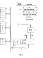
- the interpreter memory 5 is divided into a number of memory areas. In each of these memory areas, a command sequence is written in the subordinate, in particular machine-oriented programming language, which interprets an instruction in the superordinate programming language. A return instruction is programmed at the end of each memory area of the interpreter memory 5.
- the interpreter memory 5 also contains a memory area in which the command for fetching the current command of the higher-level programming language is stored. In one The last memory area at the end of the interpreter memory stores the operation part of a jump instruction.
- the microcomputer shown also contains the elements according to the invention, namely a read-only memory 7, in particular a PROM, a directly taking over memory 8 and an address decoder 6.
- the inputs of the read-only memory 7 are connected to the data bus, which has a number n of corresponding to the word width of the subordinate programming language Has lines.
- the number of addresses in the read-only memory corresponds to the operation code length OC of the higher-level programming language.
- the relationship (1) applies to the number c of the address-side address lines of the read-only memory 7:
- the read-only memory 7 contains a number of addressable memory locations in which the entry addresses for the interpreter memory 5 are permanently stored.
- the number of outputs of the read-only memory 7 corresponds to the address width AB or length for the interpretation program, which corresponds to the logarithm of the base 2 the length of the interpretation program in terms of the number of memory words.
- the outputs of the read-only memory 7 are connected to a first number AB of inputs of the directly receiving memory 8.
- the directly taking over memory 8 is preferably designed as a D register in TTL technology with tristate outputs.
- a further number of inputs AG of the D register 8 are connected to the more significant bits for the start address of the interpretation program in the address area and the remaining bits of the JUMP code of number k.
- the relationship (2) applies to the inputs AG:
- the D register 8 is controlled by the address decoder 6, which is connected on the input side to the control bus and the address bus nk in the bus structure.
- the address decoder 6 generates a load control signal for the corresponding input G of the D register 8, which is activated at the address j-1, and a read control signal for the output OE of the D register 8, which is activated at the address j.
- the addresses j-1 and j are the addresses of the modifiable JUMP instruction, which are given next to the circuit diagram.
- the word width n o corresponds to either 0 or n.
- n + k corresponds to the length of the JUMP operation code and nk to the length of the JUMP address, which in turn corresponds to the size of the address area.
- the activation of the circuit supplement of a microcomputer according to the invention is carried out by a program part which consists of a command which outputs the criterion for branching in the command code of the higher-level programming language onto the data bus of the microprocessor system, and of the unconditional jump command which effects the multiple branching.
- the jump instruction in the subordinate programming language which causes a program counter loading with a constant address, is modified via the read-only memory 7 and the D register 8 in such a way that the memory cell which is to contain the jump address has the starting address of the command to be interpreted as new jump address is overwritten before it is loaded into the program counter.
- the command in the higher-level programming language is loaded into the microprocessor.
- the microprocessor runs at address j-1 and executes a jump instruction (JUMP).
- the program counter of the microprocessor automatically switches to address j.
- the entry address interpreted by read-only memory 7 is available for the processor in D register 8.
- the program counter 3 of the microprocessor 2 is thus set to the beginning of the corresponding interpretation branch in the interpreter memory 5.
- the command in the higher-level programming language can thus be interpreted without an additional time delay.
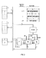
- the jump address consists of two successive memory words, each of which is permanently stored in one of the two read-only memories 8a, 8b.
- Both D registers 8a and 8b are activated at their inputs G by a charge control signal at the address j-1 and thereby take over the information pending at their data inputs.
- the data inputs AG1 of the D register 8a correspond to the remaining JUMP code bits k.
- the further data inputs n-AG1 of the read-only memory 8a are connected to part of the outputs AB of the read-only memory 7.
- the data inputs AG2 of the D register 8b are occupied with the most significant bits for the start address of the interpretation program in the address area.
- the relationship (3) applies:
- the two D registers 8a and 8b ' are connected to the data bus, where n in turn corresponds to the word length of the subordinate programming language.
- the address decoder 6 ' which in turn is connected on the input side to the control bus and the address bus 2n-k, generates a read control signal for the input OE1 of the D register 8a, which is activated at the address j, and a read control signal for the output 0E2 of the D Register 8b, which is activated at the address j + 1.
- the input circuitry of the two D-registers 8a and 8b can alternatively also be carried out in such a way that the data inputs AG1 of the D-register 8a are occupied with the remaining JUMP code bits and higher-order bits for the start address of the interpretation program in the address area and the data inputs AG2 of the D registers 8b are assigned ⁇ .
- n corresponds to either 0 or the word length n of the subordinate programming language
- n o + k corresponds to the length of the JUMP operation code
- 2n-k corresponds to the length of the JUMP address and thus the size of the address area.
Landscapes
- Engineering & Computer Science (AREA)
- Software Systems (AREA)
- Theoretical Computer Science (AREA)
- Physics & Mathematics (AREA)
- General Engineering & Computer Science (AREA)
- General Physics & Mathematics (AREA)
- Devices For Executing Special Programs (AREA)
Priority Applications (1)
| Application Number | Priority Date | Filing Date | Title |
|---|---|---|---|
| AT80105471T ATE10981T1 (de) | 1979-09-24 | 1980-09-12 | Schaltungsanordnung fuer einen mikrocomputer mit interpretorspeicher. |
Applications Claiming Priority (4)
| Application Number | Priority Date | Filing Date | Title |
|---|---|---|---|
| DE19792938570 DE2938570A1 (de) | 1979-09-24 | 1979-09-24 | Schaltungsanordnung fuer einen mikrocomputer |
| DE2938570 | 1979-09-24 | ||
| DE2942025 | 1979-10-17 | ||
| DE19792942025 DE2942025A1 (de) | 1979-10-17 | 1979-10-17 | Schaltungsanordnung fuer einen mikrocomputer |
Publications (3)
| Publication Number | Publication Date |
|---|---|
| EP0025952A2 true EP0025952A2 (fr) | 1981-04-01 |
| EP0025952A3 EP0025952A3 (en) | 1982-04-07 |
| EP0025952B1 EP0025952B1 (fr) | 1984-12-27 |
Family
ID=25781162
Family Applications (1)
| Application Number | Title | Priority Date | Filing Date |
|---|---|---|---|
| EP80105471A Expired EP0025952B1 (fr) | 1979-09-24 | 1980-09-12 | Dispositif de circuit pour un micro-calculateur avec une mémoire d'interpreteur |
Country Status (2)
| Country | Link |
|---|---|
| EP (1) | EP0025952B1 (fr) |
| DE (1) | DE3069871D1 (fr) |
Cited By (4)
| Publication number | Priority date | Publication date | Assignee | Title |
|---|---|---|---|---|
| WO1988007718A1 (fr) * | 1987-03-24 | 1988-10-06 | Insignia Solutions Limited | Agencement servant a l'emulation de logiciels |
| WO1995008800A1 (fr) * | 1993-09-23 | 1995-03-30 | Apple Computer, Inc. | Dispositif et procede de transfert de commande de programme d'emulation |
| WO1995009393A1 (fr) * | 1993-09-27 | 1995-04-06 | Apple Computer, Inc. | Appareil et procede pour emettre des instructions de programme d'emulation |
| US5574887A (en) * | 1993-09-20 | 1996-11-12 | Apple Computer, Inc. | Apparatus and method for emulation routine pointer prefetch |
Family Cites Families (2)
| Publication number | Priority date | Publication date | Assignee | Title |
|---|---|---|---|---|
| DE2201754B1 (de) * | 1972-01-14 | 1973-04-26 | Diehl Datensysteme Gmbh | Schaltungsanordnung zur interpretation des inhalts eines registers des rechenwerkes einer datenverarbeitungsanlage als befehl |
| IL42113A (en) * | 1972-04-28 | 1976-02-29 | Elliott Bros | Digital computing systems |
-
1980
- 1980-09-12 EP EP80105471A patent/EP0025952B1/fr not_active Expired
- 1980-09-12 DE DE8080105471T patent/DE3069871D1/de not_active Expired
Cited By (4)
| Publication number | Priority date | Publication date | Assignee | Title |
|---|---|---|---|---|
| WO1988007718A1 (fr) * | 1987-03-24 | 1988-10-06 | Insignia Solutions Limited | Agencement servant a l'emulation de logiciels |
| US5574887A (en) * | 1993-09-20 | 1996-11-12 | Apple Computer, Inc. | Apparatus and method for emulation routine pointer prefetch |
| WO1995008800A1 (fr) * | 1993-09-23 | 1995-03-30 | Apple Computer, Inc. | Dispositif et procede de transfert de commande de programme d'emulation |
| WO1995009393A1 (fr) * | 1993-09-27 | 1995-04-06 | Apple Computer, Inc. | Appareil et procede pour emettre des instructions de programme d'emulation |
Also Published As
| Publication number | Publication date |
|---|---|
| DE3069871D1 (en) | 1985-02-07 |
| EP0025952A3 (en) | 1982-04-07 |
| EP0025952B1 (fr) | 1984-12-27 |
Similar Documents
| Publication | Publication Date | Title |
|---|---|---|
| DE2755273C2 (fr) | ||
| DE2813128C2 (de) | Steuereinrichtung für Mikroprogrammspeicher | |
| DE3587277T2 (de) | System fuer die umgehungssteuerung beim pipelinebetrieb eines computers. | |
| EP0097725B1 (fr) | Circuits dans l'unité de commande d'un processeur microprogrammé pour l'exécution directe d'instructions sélectionnées par le hardware | |
| DE1250659B (de) | Mikroprogrammgesteuerte Datenverarbeitungsanlage | |
| DE1275800B (de) | Steuerwerk fuer datenverarbeitende Maschinen | |
| DE2134816A1 (de) | Einrichtung zur adressenuebersetzung | |
| DE2718551B2 (fr) | ||
| EP0025952B1 (fr) | Dispositif de circuit pour un micro-calculateur avec une mémoire d'interpreteur | |
| EP0130269A2 (fr) | Commande à programme mémorisé | |
| CH632349A5 (de) | Einrichtung zur mikrobefehlssteuerung. | |
| DE2938570A1 (de) | Schaltungsanordnung fuer einen mikrocomputer | |
| DE4200285A1 (de) | Microcomputer-speicherzugriffverfahren | |
| DE2744252C2 (fr) | ||
| DE1296429B (de) | Datenbearbeitungsanlage | |
| EP0494329B1 (fr) | Circuit électrique pour le mappage de l'espace d'adressage logique d'une unité de traitement vers l'espace d'adressage physique d'une mémoire | |
| DE2942025A1 (de) | Schaltungsanordnung fuer einen mikrocomputer | |
| DE2264346A1 (de) | Mehrstufiges selbstanpassendes decodiersystem fuer binaere mikrobefehle | |
| EP0375711B1 (fr) | Procede et dispositif d'exploitation d'une commande programmable en memoire | |
| DE2730796A1 (de) | Speichereinrichtung | |
| DE10128752A1 (de) | Verfahren zur Ablage von Daten in einen Speicherbaustein | |
| DE69700649T2 (de) | Leseverfahren und -anordnung mit Speicherprädiktion | |
| DE2645044A1 (de) | Speicheranordnung mit direkter adressierung | |
| DE4018419C2 (fr) | ||
| DE19640316A1 (de) | Schaltungsanordnung mit einem Mikroprozessor und einem Stapelspeicher |
Legal Events
| Date | Code | Title | Description |
|---|---|---|---|
| PUAI | Public reference made under article 153(3) epc to a published international application that has entered the european phase |
Free format text: ORIGINAL CODE: 0009012 |
|
| AK | Designated contracting states |
Designated state(s): AT BE CH DE FR GB IT LU NL SE |
|
| 17P | Request for examination filed |
Effective date: 19811028 |
|
| PUAL | Search report despatched |
Free format text: ORIGINAL CODE: 0009013 |
|
| AK | Designated contracting states |
Designated state(s): AT BE CH DE FR GB IT LU NL SE |
|
| ITF | It: translation for a ep patent filed | ||
| GRAA | (expected) grant |
Free format text: ORIGINAL CODE: 0009210 |
|
| AK | Designated contracting states |
Designated state(s): AT BE CH DE FR GB IT LI LU NL SE |
|
| REF | Corresponds to: |
Ref document number: 10981 Country of ref document: AT Date of ref document: 19850115 Kind code of ref document: T |
|
| REF | Corresponds to: |
Ref document number: 3069871 Country of ref document: DE Date of ref document: 19850207 |
|
| ET | Fr: translation filed | ||
| PG25 | Lapsed in a contracting state [announced via postgrant information from national office to epo] |
Ref country code: LU Free format text: LAPSE BECAUSE OF NON-PAYMENT OF DUE FEES Effective date: 19850930 |
|
| PLBE | No opposition filed within time limit |
Free format text: ORIGINAL CODE: 0009261 |
|
| STAA | Information on the status of an ep patent application or granted ep patent |
Free format text: STATUS: NO OPPOSITION FILED WITHIN TIME LIMIT |
|
| 26N | No opposition filed | ||
| PGFP | Annual fee paid to national office [announced via postgrant information from national office to epo] |
Ref country code: AT Payment date: 19860829 Year of fee payment: 7 |
|
| PGFP | Annual fee paid to national office [announced via postgrant information from national office to epo] |
Ref country code: NL Payment date: 19870930 Year of fee payment: 8 |
|
| PG25 | Lapsed in a contracting state [announced via postgrant information from national office to epo] |
Ref country code: GB Effective date: 19890912 Ref country code: AT Effective date: 19890912 |
|
| PG25 | Lapsed in a contracting state [announced via postgrant information from national office to epo] |
Ref country code: SE Effective date: 19890913 |
|
| PG25 | Lapsed in a contracting state [announced via postgrant information from national office to epo] |
Ref country code: LI Effective date: 19890930 Ref country code: CH Effective date: 19890930 Ref country code: BE Effective date: 19890930 |
|
| BERE | Be: lapsed |
Owner name: SIEMENS A.G. BERLIN UND MUNCHEN Effective date: 19890930 |
|
| PG25 | Lapsed in a contracting state [announced via postgrant information from national office to epo] |
Ref country code: NL Effective date: 19900401 |
|
| GBPC | Gb: european patent ceased through non-payment of renewal fee | ||
| NLV4 | Nl: lapsed or anulled due to non-payment of the annual fee | ||
| PG25 | Lapsed in a contracting state [announced via postgrant information from national office to epo] |
Ref country code: FR Effective date: 19900531 |
|
| REG | Reference to a national code |
Ref country code: CH Ref legal event code: PL |
|
| PG25 | Lapsed in a contracting state [announced via postgrant information from national office to epo] |
Ref country code: DE Effective date: 19900601 |
|
| REG | Reference to a national code |
Ref country code: FR Ref legal event code: ST |
|
| EUG | Se: european patent has lapsed |
Ref document number: 80105471.9 Effective date: 19900521 |