EP0026877A2 - Procédé et dispositif pour la corrélation de deux signaux - Google Patents
Procédé et dispositif pour la corrélation de deux signaux Download PDFInfo
- Publication number
- EP0026877A2 EP0026877A2 EP80105758A EP80105758A EP0026877A2 EP 0026877 A2 EP0026877 A2 EP 0026877A2 EP 80105758 A EP80105758 A EP 80105758A EP 80105758 A EP80105758 A EP 80105758A EP 0026877 A2 EP0026877 A2 EP 0026877A2
- Authority
- EP
- European Patent Office
- Prior art keywords
- sampling
- memory
- arrangement according
- signal
- circuit
- Prior art date
- Legal status (The legal status is an assumption and is not a legal conclusion. Google has not performed a legal analysis and makes no representation as to the accuracy of the status listed.)
- Granted
Links
Images




Classifications
-
- G—PHYSICS
- G01—MEASURING; TESTING
- G01F—MEASURING VOLUME, VOLUME FLOW, MASS FLOW OR LIQUID LEVEL; METERING BY VOLUME
- G01F1/00—Measuring the volume flow or mass flow of fluid or fluent solid material wherein the fluid passes through a meter in a continuous flow
- G01F1/66—Measuring the volume flow or mass flow of fluid or fluent solid material wherein the fluid passes through a meter in a continuous flow by measuring frequency, phase shift or propagation time of electromagnetic or other waves, e.g. using ultrasonic flowmeters
- G01F1/666—Measuring the volume flow or mass flow of fluid or fluent solid material wherein the fluid passes through a meter in a continuous flow by measuring frequency, phase shift or propagation time of electromagnetic or other waves, e.g. using ultrasonic flowmeters by detecting noise and sounds generated by the flowing fluid
-
- G—PHYSICS
- G06—COMPUTING OR CALCULATING; COUNTING
- G06F—ELECTRIC DIGITAL DATA PROCESSING
- G06F17/00—Digital computing or data processing equipment or methods, specially adapted for specific functions
- G06F17/10—Complex mathematical operations
- G06F17/15—Correlation function computation including computation of convolution operations
Definitions
- the invention relates to a method for correlating two signals, in which time-shifted samples of the two signals are multiplied with one another and the mean value of the multi-replication results corresponding to the same time shift is formed to determine a base value of the correlation function, and to an arrangement for carrying out this method.
- correlation of two different signals cross-correlation
- autocorrelation correlation of a signal with the same, but time-shifted signal
- a well-known area of application of correlation technology is the contactless speed measurement on moving objects and fluids, which is required in many branches of process and automation technology. Examples are the flow measurement in multi-phase flows or in the transport of solids in pipelines.
- Acoustic or capacitive sensors can obtain noise signals, from which one can use correlation analysis to determine the running time of the flow of the medium or the moving surface between the two sensors.
- the time shift between the correlated signals corresponding to the maximum of the cross-correlation function is in fact equal to the transit time from the first sensor to the second sensor.
- the correlator To simplify the signal processing in the correlator, it is known not to carry out the correlation on the continuous analog signals, but rather on discrete samples taken at predetermined time intervals, which are preferably brought into a digital form. Another known simplification is that only the signs of the sensor signals are evaluated in a so-called polarity correlator as signal values. In this case, the samples are binary signals that only take one or the other of two signal values.
- the previously known digital correlators are complex laboratory measuring devices based on a hard-wired computer, which, as a result, provide the entire course of the correlation function on an oscillograph screen or an XY recorder, from which the measuring technician must manually determine the position of the maximum that is of sole interest in non-contact speed measurement .
- a major disadvantage is the long computing time; the usual correlators calculate the correlation function serially, so that, for example, the calculation takes 256 N time units to calculate 256 base values and N averages per correlation base value. Only then can the maximum be determined.
- more complex laboratory correlators are known, which have 256 multiplication and integration stages operating in parallel and calculate a new estimated value for the entire correlation function in each sampling time. In this case, a maximum can be reached very early localized, but the effort is extremely large. Both methods are ruled out for an operating measuring device, the first because of the long measuring time, the second because of the technical complexity.
- runtime correlators which, with the aid of a controllable delay line, a control circuit and a voltage-controlled oscillator in a predominantly analog technique, continuously determine the runtime from the zero crossing of the differentiated correlation function using a gradient method.
- These correlators show the shortcomings of all analog techniques, such as poor integrability to a large circuit as well as temperature and long-term constancy problems.
- the principle of determining the maximum with the aid of a control is itself very critical in the multitude of practical cases of correlation functions which not only show a maximum, but also numerous secondary maxima in addition to the main maximum as a result of periodic signal components (e.g. circulation pumps in a pipeline section) .
- control loop snaps into a secondary maximum and thus results in a completely wrong measurement.
- Another problem is the detection of the standstill. In this case, the correlation function has no significant maximum, and an unordered search for the controller must be suppressed by additional devices. Due to the system-related inertia of the control loop, the sudden restart can also result in the shifting maximum falling outside the capture range.
- the object of the invention is to provide a method which enables the fast and reliable correlation of two signals with little effort, and an arrangement for carrying out the method.
- this object is achieved according to the invention in that one signal is sampled at a sampling frequency which is a multiple of the sampling frequency of the other signal, in that a number of the last samples of the slower sampled signal is stored that each sample of the faster sampled signal is simultaneously multiplied by all stored samples of the slower sampled signal and that the multiplication results corresponding to the same time shift between the multiplied samples are summed up separately.
- the main advantage of the method according to the invention is that the calculation of the correlation function is carried out simultaneously in several sampling values in each sampling time of the faster sampled signal, so that after a relatively short number of sampling periods, a calculation has been carried out for each reference value of the correlation function.
- the detection of the maximum that is formed during the averaging process can happen very early in comparison to the serial correlator.
- Such an arrangement can be constructed in a simple manner with commercially available integrated analog or digital circuits.
- a particularly advantageous embodiment consists in that the distributor circuit and the memory are formed by a microcomputer.
- An advantageous development of the method according to the invention is that in a first phase of each of several successive cycles, the n multiplication results obtained simultaneously in each sampling period of the faster sampling are written in parallel to a buffer memory in time with the fast sampling, and in a second Phase of each cycle, the multiplication results stored in the buffer memory are read out of the buffer memory in a cycle adapted to the working speed of the summation memory and are distributed to the memory locations of the summation memory.
- the frequency of the fast sampling is independent of the operating frequency of the summation memory and is only determined by the speed at which the multiplication results can be entered into the buffer memory. Even if one assumed that the buffer memory does not work faster than the summation memory, this would already mean a multiplication of the sampling frequency by a factor of n, because n multiplication results in parallel can be entered in the buffer memory. In addition, however, there is a further increase in the maximum possible sampling frequency because the groups of multiplication results can be entered into the buffer memory in unsorted order in successive memory locations and do not have to be added to the previous content.
- the calculation of the entire correlation function takes place in approximately the same time as when the multiplication results are entered directly into the summation memory, but on the basis of samples which are obtained with a much higher sampling frequency.
- scanning frequencies of approximately 50 kHz can be achieved with commercially available microcomputer components.
- FIG. 1 shows, as an application example for a correlation system, an arrangement for measuring the flow velocity v of a medium in a pipeline 1.
- Two sensors 2 and 3 are attached to the pipeline 1 at a precisely known distance D, which extract noise signals from the flowing medium and corresponding ones deliver electrical signals x (t) or y (t).
- the sensors can be of any type, for example optical, acoustic or capacitive sensors.
- the flow velocity v in the pipeline 1 can be determined by forming the cross-correlation function R (T) between the two signals x (t) and y (t). This is due to the fact that the signals generated when the same flow components (vortices) pass by the two sensors 2 and 3 have certain similarities which result in a maximum in the cross-correlation function.
- the cross correlation function has the mathematical form
- the instantaneous values of the signal x (t) are multiplied by the instantaneous values of the signal y (t) shifted by a shift time T and the mean value of the products is formed over the range of the observation time T.
- a base value of the correlation function is obtained for each value of the displacement time T.
- the correlation function has a maximum at a specific displacement time TM , which is the same as the transit time of the medium from sensor 3 to sensor 2, so if:
- the correlation function is determined by a correlator 4.
- An evaluation device 5 connected to the correlator 4 examines the correlation function to a maximum and outputs the corresponding displacement time T M or the flow velocity v calculated therefrom.
- the correlator 4 does not calculate the correlation function directly from the analog signals x (t) and y (t), but for simplification according to a method known per se from their sign; it is a so-called polarity correlator.
- the sensor 2 is followed by a signal converter 6, which emits a binary signal S x (t) at the output, which assumes a signal value corresponding to the binary value 0 (for example the voltage zero) when the signal x (t) is negative, and a signal value corresponding to the binary value 1 (for example a positive voltage value) if the signal x (t) is positive.
- these signal values are referred to below as "signal value 0" or "signal value. 1".
- each signal converter 6, 7 can be a threshold value generator, which is formed, for example, by an operational amplifier that is not fed back, and whose threshold value is set to zero. It is also possible to choose a non-zero threshold; in this case, a binary signal is also obtained at the output of each signal converter 6, 7, but is not a sign signal.
- sampling circuits 8, 9 are shown in FIG. 1, which are inserted between the outputs of the signal converters 6, 7 and the correlator 4 and are controlled by clock pulses which are supplied by a clock generator 10.
- the sampling circuits 8, 9 are designed such that they each save the signal value present at the signal input when a clock pulse is received and make it available as a sample value X or Y until the next clock pulse.
- the sampling of the sign signals S y (t) and S x (t) thus takes place in the frequency ratio 1: k, and k samples X of the sign signal S x (t) are obtained for a sample Y of the sign signal S y (t).
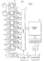
- Fig. 2 shows an embodiment of the correlator 4 of Fig. 1.
- the sampling circuits are included in the correlator; the correlator therefore receives the binary sign signals S x (t) and Sy (t) at two inputs 12, 13, which are supplied by the signal converters 6, 7.
- the correlator contains a one-stage X register 14, the only register stage of which is formed by a D flip-flop, the D input of which is connected to the input 12 and the clock pulses I c from the clock generator 10 are applied to its clock input.
- the Q output on the rising edge of each clock pulse I c assumes the signal value present at the instant at the D input, which it maintains until the next clock pulse I c .
- the X register 14 plays the role of the sampling circuit 8 of FIG. 1 and provides the samples X obtained by the successive samples at the output. This simple design of the sampling circuit is possible because the sign signal S x (t) to be sampled is a binary signal.
- the correlator also contains a multi-stage Y register 15 with eight register stages 15a to 15h, which are also formed by D flip-flops.
- the Y register 15 is designed as a shift register in that the Q output of each of the register stages 15a to 15g is connected to the D input of the following register stage 15b to 15h, while the clock inputs of all register stages 15a to 15h are connected in parallel to the output of the frequency divider 11 are connected.
- the D input of the first register stage 15a is connected to the input 13.
- the same clock pulse I c ' which effects the sampling of the sign signal S y (t) in the register stage 15a, also triggers the transfer of the content of each of the register stages 15a to 15g to the next register stage 15b to 15h.
- the sample value Y a obtained with the last sampling pulse I c ' is available: at the output of the register stage 15b, a sample value Y b is available which corresponds to the previous clock pulse I c 'has been sampled, and in a corresponding manner, sample values Y c to Y h are available at the outputs of the register stages 15c to 15h, each of which is earlier by a period of the clock pulses I c ' than the sample value in the previous register stage.
- the eight most recent samples of the sign signal S y (t) are stored in the Y register 15 at the same time, and they are available in parallel at the outputs of the eight
- the eight register stages 15a to 15h of the Y register 15 are assigned eight multipliers 16a to 16h, each of which is connected at the first input to the Q output of the D flip-flop of the associated register stage 15a to 15h, while the second inputs of all eight multipliers 16a to 16h are connected in parallel to the Q output of the D flip-flop of the X register 14. Since the signals to be multiplied are simple binary signals, each of the multipliers 16a to 16h is formed by a digital logic circuit. In the example shown, each multiplier is an equivalent circuit, i.e. a digital logic circuit which delivers the signal value 1 at the output if its two input signals have the same signal value (O or 1), while the output signal has the signal value 0 if the two input signals have different signal values.
- the outputs of the multipliers 16a to 16h are connected to the inputs of a distributor circuit 17, which inputs the binary signals supplied by the multipliers as multiplication results into the memory locations of a summation memory 18 in a manner explained later.
- the distributor circuit 17 can be synchronized, for example, by the clock pulses I c of the clock generator 10.
- Each memory location of the memory 18 has a capacity of several bits, and the design is such that the bits successively entered in the same memory location can each be added to the previous content. As will be explained later, the content of each memory location represents a base value of the correlation function.
- a memory query circuit 19 connected to the memory 18 enables the memory locations to be queried and thereby the correlation function to be obtained.
- the output of the memory interrogation circuit 19 is connected to the evaluation device 5 (FIG. 1).
- the frequency divider 11 can be a 5-stage binary counter.
- the distributor circuit 17, the memory 18 and the memory interrogation circuit 19 are preferably formed by a microcomputer with the word length of n bits, which is programmed accordingly.
- Table I at the end of the description shows the sample values X and Y appearing in the course of several successive sampling cycles in the X register 14 and in the Y register 15.
- the sampling times which correspond to the periods of the clock pulses I c are indicated at the top of the table . These sampling times are denoted by t 0 , t 1 , t 2 ..., starting from any sampling time t 0 , in which a pulse I c and a pulse I c 'appear simultaneously.
- a sampling cycle corresponds to one period of the slow clock pulses I c ', ie 32 periods of the fast clock pulses I c . For reasons of space, only the first and last sampling times in each sampling cycle are shown.
- the samples X and Y are provided with an index which denotes the sampling time in which the sample was sampled. For each sampling time t0, t1, t2 ... appears in the X-register 14, a sample X 0, X 1, X 2 ..., which carries the same index as the sampling time.
- stage 15b The sample value, which was previously in stage 15a, was transferred to stage 15b at the beginning of the sampling time t. This sample was obtained 32 sample times earlier and is accordingly designated Y -32 . The sample value Y -32 remains at the end of the sampling cycle at the output of stage 15b.
- samples Y- 64 ' Y- 96 ' Y- 128 ' Y- 160' Y- 192 ' Y -224' exist at the outputs of stages 15c to 15h during the entire sampling cycle, each by 32 Ab sampling times have been obtained earlier than the sample in the previous stage.
- the next sampling cycle begins with sampling time t 32 .
- a clock pulse I c 'appears again at the same time as a clock pulse I c , so that a new sample value Y 32 appears in stage 15a of the Y register 15 simultaneously with the sample value X 32 in the X register 14.
- the previous contents of the stages of the Y register 15 are shifted by one stage, so that the sample Y is now in stage 15b, the sample Y -32 in stage 15c, etc.
- next sampling time t 32 which is the first sampling time of the following sampling cycle
- the corresponding eight multiplication results are stored in the eight memory locations No. 0, No. 32, No. 64, No. 96, No. 128, No. 160, No. 192, No. 224 entered, which already contain the multiplication results of the previous sampling cycle.
- the new multiplication results are added to the content of the storage locations without being deleted. The same process is repeated for the following sampling times of this sampling cycle, the contents of the storage locations either remaining unchanged or being increased by one unit, depending on the multiplication result.
- each memory location is assigned to a specific time shift between the samples multiplied with one another and the products of sample values that always correspond to the same time shift are summed in each memory location, the content of each memory location obviously corresponds to a base value of the correlation function.
- a correlation function R x y ( T ) as a function of the displacement time T is plotted on the head of FIG. 3.
- This diagram shows the calculation of the base values in the successive sampling cycles, only four sampling times being shown for simplification in each sampling cycle.
- the timeline is vertically down.
- the calculation of the support values in the sampling time t 15 in the middle of the sampling cycle and in the last sampling time t 31 is also shown as an example.
- a second calculation is carried out for the same base values. If a multiplication result 1 is entered into a memory cell into which a result 1 has already been entered in the previous sampling cycle, a second point is added to the already existing black point.
- the memory locations can be searched for by the evaluation device 5 at predetermined intervals with the aid of the memory query circuit 19, the correlation function consisting of discrete base values possibly by interposing a filter 20 can be smoothed.
- the filter 20 can be implemented by appropriate programming (software filter). If a sufficiently significant correlation maximum has been recognized, either the correlation time Tm or the converted speed is output. Then a new measuring cycle starts, whereby either the memory 18 is erased (summing operation) or the numerical values in the memory are divided by a constant amount and these numerical values are assumed (smooth operation).
- the time shift ⁇ M at which the maximum of the correlation function occurs, the duration of the flow medium from the sensor 3 corresponds to the sensor 2.
- This term is obtained as a multiple of a T in a measuring range of from O to m ⁇ ⁇ goes from 0 to 255 ⁇ in the example described.
- O T the measuring range can therefore be set and changed as desired.
- ⁇ is equal to the period of the clock 10
- the measurement range can be determined in a very simple manner by a corresponding setting of the frequency of the clock 10.
- the clock 10 is therefore preferably designed so that its frequency is adjustable.
- the frequency can either be set manually by an operator or automatically by a control signal, which is applied, for example, by the evaluation device 5 to a frequency control input 10a of the clock generator 10.
- a control signal which is applied, for example, by the evaluation device 5 to a frequency control input 10a of the clock generator 10.
- Such an automatic frequency control is particularly advantageous when the evaluation device 5, together with the circuit components 17, 18, 19, 20, is formed by a microcomputer.
- the clock pulses I c are preferably supplied by the microcomputer, so that the clock 10 is also part of the microcomputer.
- the microcomputer it is then possible to adapt the measuring range to the investigated speed range in order to place the maximum of the correlation function in a favorable range and to optimally use the resolving power of the correlator. For example, after a first approximate determination of the position of the correlation maximum, the correlation function can be spread by increasing the frequency of the clock generator 10 so that only the area containing the maximum is examined.
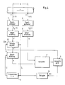
- FIG. 4 shows a further development of the arrangement from FIG. 1, with which this pre-delay can be obtained for the case considered here that the correlated signals are samples of binary signals.
- the signal converter 7 is followed by a sampling circuit 21, which is clocked by the fast clock pulses I c , and a shift register 22, likewise clocked by the fast clock pulses I c, is inserted between the sampling circuit 21 and the sampling circuit 9.
- sample values Y 'appear synchronously with the sample values X and with the same fast repetition frequency as this.
- These delayed samples Y' with respect to the samples Y then removes the sampling circuit 9 with the slow repetition frequency of the pulses I ', the sample values Y, which are stored in the Y register 15 (FIG. 2) and multiplied by the sample values X.
- the output of the shift register 22 is connected to the terminal 13 when the development shown in FIG. 4 is used. Otherwise the circuit of FIG. 2 remains unchanged.
- the pre-delay given by the shift register 22 has the effect that there are shift times between the sample values X appearing in the X register 14 and the sample values Y a to Y h in the Y register 15, which are each longer by q ⁇ ⁇ than the shift times which were previously explained for the embodiment of FIGS. 1 and 2 and are listed in Table II.
- the measuring range no longer ranges from 0 ⁇ to 255 ⁇ , but from q ⁇ ⁇ to (225 + q) ⁇ .
- the pre-delay given to the slower sampled signal can be adjusted, which can be achieved in the embodiment of FIG. 4 by using a shift register 22 in which the number q of the stages which come into effect by one to one Control input 22a applied control signal is changed.
- a shift register 22 in which the number q of the stages which come into effect by one to one Control input 22a applied control signal is changed.
- This setting of the pre-delay can in turn be carried out manually by an operator, or also automatically by a control signal which is applied by the evaluation device 5 to the control input 22a, as shown in FIG. 4. If the correlator 4 and the evaluation device 5 are formed by a microcomputer, this can, for example after the first determination of a correlation maximum that exceeds a predetermined minimum value, set the pre-delay so that the maximum is shifted to the center of the measuring range, and then the frequency of the clock generator 10 so that the section containing the maximum is spread over the entire measuring range.
- the pre-delay of the slower sampled signal can of course also be obtained in other ways. It can also be given directly to the analog signal y (t), for example with the aid of a delay line.
- sampling circuits are designed as analog circuits, at for example in the form of the known instantaneous value memories ("Sample &Hold"), each sampling circuit is followed by an analog-to-digital converter which converts the analog sample value into a multi-digit binary number representing the amount and sign.
- Each register stage of registers 14 and 15 in FIG. 2 is then designed such that it can store a multi-digit binary number which represents the sample in question.
- multipliers 16a to 16h are used, which are suitable for multiplying binary digits.
- Such a multi-digit design of the circuit described does not present any difficulty to the person skilled in the art.
- the Y register and the multipliers are also carried out using analog technology;
- the Y register can be formed by an analog shift register in the manner of the charge-coupled arrangements (bucket chain circuits). Since a digital memory is preferably used for the storage and summation of the multiplication results, analog-to-digital converters are inserted between the outputs of the analog multipliers and the inputs of the distribution circuit, which in the case of processing sign signals again simple threshold value transmitters and multi-digit processing are quantization and coding circuits.
- the maximum frequency of the fast sampling is limited by the operating speed of the summation memory 18.
- the frequency f of the fast sampling must namely be dimensioned such that the n multiplication results obtained in each sampling period are stored in the assigned memory locations of the summation memory 18 below Addition to the previous content can be entered. If the correlator contains a microcomputer as distribution circuit 17, maximum sampling frequencies of only about 1000 Hz can be achieved. This results in a limitation of the method to relatively low-frequency signals, so that in some applications the resolution of the correlation maximum and thus the measurement accuracy do not meet the requirements.
- FIGS. 5 to 7 A modified embodiment of the correlator is shown in FIGS. 5 to 7, which enables the calculation of the correlation function in approximately the same time as with the embodiment of FIG. 2, but on the basis of sample values which are obtained with a much higher sampling frequency.
- the outputs of the multipliers 16a to 16h in FIG. 5 are connected to the data inputs of a buffer memory 30, to which an address counter 31 is assigned.
- Each storage location has a capacity which is sufficient to accommodate the multiplication results simultaneously supplied by the multipliers 16a to 16h. Since in the example of a polarity correlator described each multiplication result is represented by one bit, each memory location of the buffer memory 30 therefore requires a capacity of 8 bits.
- the address counter 31 is designed as a "modulo 32" counter.
- the address counter 31 has a clock input which is connected to the output of an OR circuit 39.
- One input of the OR circuit 39 is connected to the output of a gate circuit 34, the signal input of which receives the fast clock signals I c from the clock generator 10.
- the control input of the gate circuit 34 is connected to an output 35a of a control circuit 35, which is also connected to a release input of the write-in circuit 32 and to a lock input of the read circuit 33.
- An index counter 36 receives the clock pulses I c so that it counts these clock pulses.
- the index counter 36 is designed as a “modulo k” counter, in the present case as a “modulo 32” counter, which is reset to the zero state after the counting of 32 clock pulses I c . It works synchronously with the frequency divider 11, so that it goes from the counter reading 31 to the counter reading zero when the frequency divider 11 outputs a pulse I c 'at the output.
- the index counter can also be formed by the frequency divider 11 if this is - as usual - a five-stage binary counter. The count of the index counter shows the number of each fast sampling period of the pulses I c within each slow sampling period of the pulses I c '.
- the stage outputs of the index counter 36 are connected to the inputs of an index register 37 which has a trigger input which is connected to a further output 35b of the control circuit 35.
- the control circuit 35 applies a short pulse to the trigger input of the index register 37, the current count of the index counter 36 is transferred to the index register 37.
- the stage outputs of the index register 37 are connected to corresponding inputs of an address computer 38, which receives the address representative output signals of the address counter 31 at a second input group.
- the outputs of the read circuit 33 of the buffer memory 30 are connected to the inputs of the distributor circuit 17, which inputs the signals read out from the buffer memory 30 into those memory locations of the summation memory 18 which are determined by the addresses supplied by the address computer 38.
- the transfer of the stored data from the buffer memory 30 is controlled by clock signals which are supplied by an output 35c of the control circuit 35.
- the output 35c is connected to the second input of the OR circuit 39, a clock input of the address computer 38 and a clock input of the distributor circuit 17.
- the memory query circuit 19 connected to the memory 18 enables the memory locations to be queried and thereby the correlation function to be obtained.
- the output of the memory interrogation circuit 19 is connected to the evaluation device 5.
- phase II begins, in which the multiplication results stored in the buffer memory 30 are arranged in the summation memory 18 via the distributor circuit 17 and added to the previous content of the relevant memory locations.
- This transmission takes place in a cycle which is determined by the control circuit 35 in accordance with the operating speed of the summation memory 18 and the associated circuits.
- This clock can be significantly slower than the clock determined by the fast sampling frequency f c .
- control circuit 35 At the beginning of phase I of each cycle, the control circuit 35 outputs a short pulse at the output 35b, which causes the current count of the index counter 37 to be transferred to the index register 38. In this way, the number of the fast sampling period that marks the beginning of phase I is recorded. This measure makes it possible to start the cycle at any point in time within a slow sampling period.
- the control circuit 35 emits a signal at the output 35a which remains for the entire duration of phase I. This signal opens the gate circuit 34, releases the write-in circuit 32 of the buffer memory 30 and blocks the read circuit 33.
- the address counter 31 has been reset to zero at the end of the previous cycle.
- the address counter 31 is advanced by the fast scanning pulses I c .
- the fast sampling frequency f c is thus only limited by the frequency with which bit groups can be entered into successive memory locations of the buffer memory 30.
- Phase I ends when the buffer memory 30 is full, i.e. when the address counter 31 changes from the counter reading 31 to the counter reading 0.
- the signal emitted at the output 35a of the control circuit 35 then assumes a value which causes the gate circuit 35 and the write-in circuit 32 to be blocked and the read circuit 33 to be released.
- the sampling circuits 14, 15 and the multipliers 16a to 16h continue to operate in the manner described above under the control of the clock pulses I c and I c ; however, the multiplication results provided by the multipliers 16a to 16h are ignored due to the blocking of the write-in circuit 32.
- the index counter 36 continues to be advanced by the fast clock pulses I c , so that its counter reading indicates the number of the fast clock period within the currently running slow clock period at all times.
- control circuit 35 outputs clock pulses at the output 35c which are fed to the clock inputs of the address counter 31, the address computer 38 and the distributor 17.
- These clock pulses have a repetition frequency which is adapted to the operating speed of the summation memory 18 and which can be substantially lower than the repetition frequency f of the fast clock pulses I C.
- the content of the memory location 30-0 which is identified by the address 0 in the address counter 31, is removed by means of the read circuit 33 and fed to the distributor 17.
- the distributor 17 arranges these eight base values in the assigned memory locations of the summation memory 18.
- the 256 memory locations of the summation memory 18 are designated 18-0, 18-1, ... 18-255.
- storage location 18-0 is assigned to the support point with the shift time 0 ⁇
- storage location 18-1 to the support point with the shift time 1 ⁇
- etc. up to storage location 18-255, that of the support point with the shift time 255 h T is assigned.
- the number of the first fast sampling period of phase I in the index register identifies the shift times for which the base values obtained in this sampling period and stored in memory location 30-0 of the buffer memory 30 have been obtained.
- the addresses of these storage locations are calculated by the address computer 38 and communicated to the distributor 17.
- FIG. 7 An embodiment of the address computer 38 is shown in FIG. 7. It contains a "modulo 32" adder 40 which receives the output signals of the address counter 31 and the index register 37 at two input groups.
- the output of the "modulo 32" adder 40, which supplies the "modulo 32" sum of the input signals, directly represents the first output 38a of the address computer 38. This output provides the memory address at which the first reference value is in each case from the buffer memory 30 taken group of eight base values in the summation memory 18 is to be classified.
- adder circuits 41, 42, 43, 44, 45, 46, 47 are connected in cascade to the output of the "modulo 32" adder 40.
- the second inputs of this adder circuits continuously receive a signal representing the number "32".
- the outputs of these adder circuits form the outputs 38b, 38c, ... 38h of the address computer.
- the distributor 17 arranges the eight base values of each base value group one after the other at the addresses specified by the address computer 38 in the summation memory 18. Only when this process has been completed does the control circuit 35 output the next clock pulse at the output 35c.
- the content of the address counter 31 is brought to 1 by this clock pulse.
- the reading circuit 33 therefore takes the content of the memory space 30-1.
- the address computer 38 calculates the new addresses on the basis of the new counter reading of the address counter 31, that is, the addresses in the previously selected example, 30, 62, 94, 126, 158, 190, 222, 254.
- the distributor 17 orders the eight extracted base values into the corresponding memory locations of the summation memory 18.
- the address computer When the address counter 31 reaches the counter reading 3, the address computer does not supply the address 32 at the output 38a, but - since the adder circuit 40 is designed as a "modulo 32" adder - the address 0.
- the addresses 32, 64, 96, 128, 160, 192, 224 At the other outputs 38b, 38c, .. . 38h appear consequently, the addresses 32, 64, 96, 128, 160, 192, 224.
- These addresses are the shift times 0 T A, T 32 A, 224 A ... T assigned, which is correct because the space from the 30-3 of the buffer memory 30 extracted sample group belongs to fast sampling cycle no. 0 of the next slow sampling cycle.
- phase II all 256 base values are successively taken from the buffer memory 30 and brought into the summation memory 18.
- Phase II has ended when the last base value group has been removed from memory location 30-31 and has been assigned to memory 18.
- the address counter 31 then goes to 0, and the control circuit 35 can initiate phase I of the next cycle in the manner described above, in which in turn receive 256 base values in time with the fast sampling, stored in the buffer memory 30 and then in the summation memory 1-8 be introduced.
- the described mode of operation enables a much higher fast sampling frequency f than in the case of direct input of the multiplication results into the summation memory 18, such as. it is applied to the correlator of FIG. 2.
- the fast sampling frequency can only be as large as the repetition frequency of the clock pulses at the output 35c of the control circuit 35. This repetition frequency must be dimensioned such that eight information in succession in different storage locations of the summation memory 18 in addition to the previous content in each clock period can be entered.
- the fast sampling frequency can be at least n times (in this case eight times) higher, because in each fast cycle period 8 support values are entered in parallel in the buffer memory 30.
- the index counter 36 and the index register 37 gives the advantage that phase I of each cycle can be initiated at any point in time, so that no waiting time elapses after phase II of the previous cycle has ended.
- the index counter 36 and the index register 37 can be omitted; this presupposes that the control circuit 35 initiates phase I in the fast sampling period No. 0 of a slow sampling period. This can easily be done, for example, by triggering the cycle in the control circuit 35 by the next slow clock pulse I C.
- the "modulo 32" adder 40 can then also be omitted in the address computer 38, so that the output 38a is formed directly by the output of the address counter 31, to which the adders 41 to 47 are also connected.
- the described principle of buffering by means of the buffer memory 30 is not limited to the case in which the base values are formed by multiplying binary samples of sign signals and therefore each consist of only one bit. It is readily suitable for the case in which the sampling circuits 14, 15 are designed in such a way that they supply multi-digit binary sampling values which represent the magnitude and sign of the sampled signal value. In this case, only the buffer memory 30 has to be designed such that each memory location can accommodate n multi-digit binary code groups in assigned sections.
- the modification of the address computer 38 required for this does not present any difficulties to the person skilled in the art.
- the circuit components of the correlator of FIG. 5, in particular the buffer memory 30, the address counter 31, the control circuit 35, the index counter 37, the address calculator 38, the distributor 17 and the summation memory 18, can of course also be formed by a suitably programmed microcomputer.
- the buffer memory 30 is preferably an area of the working memory (RAM) of the microcomputer.
- the correlation method described above is of course not limited to the cross-correlation of two different signals in the correlative speed measurement given as an example. It is basically suitable for all areas of application in which the cross-correlation of two different signals or the auto-correlation of a signal with itself is to be carried out.
- the signal x (t) simply replaces the signal y (t) in all the exemplary embodiments described above.
Landscapes
- Physics & Mathematics (AREA)
- Engineering & Computer Science (AREA)
- General Physics & Mathematics (AREA)
- Mathematical Physics (AREA)
- Computational Mathematics (AREA)
- Theoretical Computer Science (AREA)
- Mathematical Analysis (AREA)
- Mathematical Optimization (AREA)
- Pure & Applied Mathematics (AREA)
- Data Mining & Analysis (AREA)
- Algebra (AREA)
- Databases & Information Systems (AREA)
- Software Systems (AREA)
- General Engineering & Computer Science (AREA)
- Computing Systems (AREA)
- Electromagnetism (AREA)
- Fluid Mechanics (AREA)
- Complex Calculations (AREA)
Applications Claiming Priority (4)
| Application Number | Priority Date | Filing Date | Title |
|---|---|---|---|
| DE2940158 | 1979-10-03 | ||
| DE19792940158 DE2940158C2 (de) | 1979-10-03 | 1979-10-03 | Verfahren und Anordnung zur Korrelation von zwei Signalen |
| DE19803030438 DE3030438A1 (de) | 1980-08-12 | 1980-08-12 | Verfahren und anordnung zur korrelation von zwei signalen |
| DE3030438 | 1980-08-12 |
Publications (3)
| Publication Number | Publication Date |
|---|---|
| EP0026877A2 true EP0026877A2 (fr) | 1981-04-15 |
| EP0026877A3 EP0026877A3 (en) | 1981-05-13 |
| EP0026877B1 EP0026877B1 (fr) | 1983-10-05 |
Family
ID=25781341
Family Applications (1)
| Application Number | Title | Priority Date | Filing Date |
|---|---|---|---|
| EP80105758A Expired EP0026877B1 (fr) | 1979-10-03 | 1980-09-25 | Procédé et dispositif pour la corrélation de deux signaux |
Country Status (2)
| Country | Link |
|---|---|
| US (1) | US4430722A (fr) |
| EP (1) | EP0026877B1 (fr) |
Cited By (3)
| Publication number | Priority date | Publication date | Assignee | Title |
|---|---|---|---|---|
| FR2562259A1 (fr) * | 1984-03-28 | 1985-10-04 | Centre Nat Rech Scient | Procede et dispositif de mesure par correlation, en temps reel, de retards entre des signaux electriques se correspondant |
| EP0194643A3 (en) * | 1985-03-13 | 1990-03-21 | Mitsubishi Denki Kabushiki Kaisha | Correlation time-difference detector |
| EP0507087A3 (en) * | 1991-03-07 | 1993-05-19 | Abb Patent Gmbh | Method and apparatus for correlative digital signal processing using systolic arithmetic circuit |
Families Citing this family (11)
| Publication number | Priority date | Publication date | Assignee | Title |
|---|---|---|---|---|
| US4509131A (en) * | 1982-06-01 | 1985-04-02 | The United States Of America As Represented By The Secretary Of The Navy | Geomagnetic velocimeter |
| US4558422A (en) * | 1983-03-23 | 1985-12-10 | Tektronix, Inc. | Digital signal sampling system with two unrelated sampling timebases |
| US4787252A (en) * | 1987-09-30 | 1988-11-29 | Panametrics, Inc. | Differential correlation analyzer |
| DE4009610A1 (de) * | 1990-03-26 | 1991-10-02 | Philips Patentverwaltung | Schaltungsanordnung zur bestimmung der lage von extremalen werten einer aehnlichkeitsfunktion |
| US5848099A (en) * | 1996-05-30 | 1998-12-08 | Qualcomm Incorporation | Method and system for testing phase imbalance in QPSK receivers |
| US6421785B1 (en) * | 1998-11-03 | 2002-07-16 | Intel Corporation | Clock selection for processing audio data |
| US6546344B1 (en) | 1999-07-02 | 2003-04-08 | Banner Engineering Corporation | Magnetic anomaly sensor system |
| US7395286B1 (en) * | 2004-01-05 | 2008-07-01 | National Semiconductor Corporation | Method for generating non-overlapping N-phases of divide-by-N clocks with precise 1/N duty ratio using a shift register |
| JP2008003466A (ja) * | 2006-06-26 | 2008-01-10 | Mitsutoyo Corp | レンズ光学系及び光電式エンコーダ |
| EP2626696A1 (fr) * | 2012-02-10 | 2013-08-14 | Acosense AB | Système de mesure acoustique avec tampon circulaire |
| US10502601B2 (en) * | 2017-01-10 | 2019-12-10 | Expro Meters, Inc. | Detection of flow rate over dynamic range |
Family Cites Families (11)
| Publication number | Priority date | Publication date | Assignee | Title |
|---|---|---|---|---|
| FR2100550B2 (fr) | 1970-05-26 | 1973-05-25 | Commissariat Energie Atomique | |
| FR1493450A (fr) | 1966-04-25 | 1967-09-01 | Commissariat Energie Atomique | Perfectionnements aux corrélateurs |
| GB1317243A (en) | 1969-05-28 | 1973-05-16 | Solartron Electronic Group | Real-time correlator |
| GB1316100A (en) | 1969-05-28 | 1973-05-09 | Solartron Electronic Group | Chain-code correlator |
| US4019038A (en) | 1971-06-10 | 1977-04-19 | Kent Instruments Limited | Correlators |
| FR2206872A5 (fr) * | 1972-10-17 | 1974-06-07 | Commissariat Energie Atomique | |
| NL165895C (nl) * | 1973-06-13 | 1981-05-15 | Philips Nv | Digitale signaalverwerkingsinrichting ter realisatie van een vooraf bepaalde overdrachtskarakteristiek. |
| GB1477833A (en) * | 1973-08-24 | 1977-06-29 | Nat Res Dev | Apparatus for comparing two binary signals |
| CA1065060A (fr) | 1976-04-01 | 1979-10-23 | Canadian General Electric Company Limited | Circuit correlateur |
| DE2633565A1 (de) * | 1976-07-27 | 1978-02-02 | Bosch Gmbh Robert | Verfahren und einrichtung zur beruehrungslosen geschwindigkeitsmessung |
| US4244026A (en) | 1978-11-06 | 1981-01-06 | General Electric Company | Velocity measuring correlation sonar |
-
1980
- 1980-09-25 EP EP80105758A patent/EP0026877B1/fr not_active Expired
- 1980-09-26 US US06/191,351 patent/US4430722A/en not_active Expired - Lifetime
Cited By (4)
| Publication number | Priority date | Publication date | Assignee | Title |
|---|---|---|---|---|
| FR2562259A1 (fr) * | 1984-03-28 | 1985-10-04 | Centre Nat Rech Scient | Procede et dispositif de mesure par correlation, en temps reel, de retards entre des signaux electriques se correspondant |
| EP0161996A1 (fr) * | 1984-03-28 | 1985-11-21 | Centre National De La Recherche Scientifique (Cnrs) | Procédé et dispositif de mesure par corrélation, en temps réel, de retards entre des signaux électriques statistiquement semblables |
| EP0194643A3 (en) * | 1985-03-13 | 1990-03-21 | Mitsubishi Denki Kabushiki Kaisha | Correlation time-difference detector |
| EP0507087A3 (en) * | 1991-03-07 | 1993-05-19 | Abb Patent Gmbh | Method and apparatus for correlative digital signal processing using systolic arithmetic circuit |
Also Published As
| Publication number | Publication date |
|---|---|
| US4430722A (en) | 1984-02-07 |
| EP0026877B1 (fr) | 1983-10-05 |
| EP0026877A3 (en) | 1981-05-13 |
Similar Documents
| Publication | Publication Date | Title |
|---|---|---|
| EP0026877B1 (fr) | Procédé et dispositif pour la corrélation de deux signaux | |
| DE1919345C3 (de) | Rahmensynchronisiervorrichtung für einen orthogonalen oder biorthogonalen Decoder | |
| DE3001499C2 (fr) | ||
| EP0084592A1 (fr) | Procédé et dispositif pour mesurer l'intevalle de temps entre les instants d'échantillonnage de deux signaux échantillonnés, en particulier des signaux d'entrée et de sortie d'un convertisseur de fréquence d'échantillonnage | |
| DE2138042A1 (de) | Numerische Werkzeugmaschinensteue rungen | |
| DE3690624C2 (fr) | ||
| DE2044711A1 (de) | Datenverarbeitungsverfahren und System zu seiner Durchfuhrung | |
| DE4331375C2 (de) | Pseudozufällig sich wiederholendes Abtasten eines Signals | |
| DE2711426C3 (de) | Frequenzvervielfacher | |
| DE2152687B2 (de) | Verfahren und Einrichtung zum Erkennen einer vorbestimmten Frequenz in einem Frequenzgemisch | |
| DE1150537B (de) | Geraet zur Umformung von Analogdaten in ziffernmaessige Daten | |
| DE1920727B2 (de) | Digitales Frequenzmeßgerät mit selbsttätiger Meßdauerbestimmung | |
| DE2625287A1 (de) | Korrelationseinrichtung und damit ausgeruestetes system zum messen der verzoegerung zwischen zwei signalen | |
| DE1190231B (de) | Anordnung zur Bestimmung der zeitlichen Mittelwerte von Funktionen | |
| DE2264203A1 (de) | System zur gasstroemungsberechnung | |
| DE1938090C2 (de) | Analysator von Massenspektren | |
| DE2923999A1 (de) | Korrelationsverfahren | |
| DE2453247B2 (de) | Anordnung zur digitalen frequenzmessung | |
| DE3882364T2 (de) | Verfahren und gerät zum lesen von zeichen. | |
| DE2615162B1 (de) | Schaltungsanordnung zur Linearisierung der Ausgangssignale von Messfuehlern | |
| DE2940158A1 (de) | Verfahren und anordnung zur korrelation von zwei signalen | |
| DE3030438C2 (fr) | ||
| DE2840065C2 (de) | Schaltungsanordnung zur Erzeugung einer Abtastimpulsfolge für ein periodisches Signal | |
| DE2629740C3 (de) | Verfahren zur Ermittlung der größten Ähnlichkeit und der Verschiebezeit bis zum Auftreten der größten Ähnlichkeit zwischen zwei über Eingabemittel in zwei parallelgeschaltete Schieberegister eingeschriebenen binaren Signalfolgen sowie eine Einrichtung zur Durchfuhrung des Verfahrens | |
| DE2200744A1 (de) | Verfahren und Vorrichtung zum Aussortieren |
Legal Events
| Date | Code | Title | Description |
|---|---|---|---|
| PUAI | Public reference made under article 153(3) epc to a published international application that has entered the european phase |
Free format text: ORIGINAL CODE: 0009012 |
|
| PUAL | Search report despatched |
Free format text: ORIGINAL CODE: 0009013 |
|
| AK | Designated contracting states |
Designated state(s): CH FR GB IT NL SE |
|
| AK | Designated contracting states |
Designated state(s): CH FR GB IT NL SE |
|
| 17P | Request for examination filed |
Effective date: 19810604 |
|
| ITF | It: translation for a ep patent filed | ||
| GRAA | (expected) grant |
Free format text: ORIGINAL CODE: 0009210 |
|
| AK | Designated contracting states |
Designated state(s): CH FR GB IT LI NL SE |
|
| ET | Fr: translation filed | ||
| PLBE | No opposition filed within time limit |
Free format text: ORIGINAL CODE: 0009261 |
|
| STAA | Information on the status of an ep patent application or granted ep patent |
Free format text: STATUS: NO OPPOSITION FILED WITHIN TIME LIMIT |
|
| 26N | No opposition filed | ||
| ITTA | It: last paid annual fee | ||
| EAL | Se: european patent in force in sweden |
Ref document number: 80105758.9 |
|
| PGFP | Annual fee paid to national office [announced via postgrant information from national office to epo] |
Ref country code: SE Payment date: 19960819 Year of fee payment: 17 |
|
| PGFP | Annual fee paid to national office [announced via postgrant information from national office to epo] |
Ref country code: FR Payment date: 19960827 Year of fee payment: 17 Ref country code: CH Payment date: 19960827 Year of fee payment: 17 |
|
| PG25 | Lapsed in a contracting state [announced via postgrant information from national office to epo] |
Ref country code: SE Free format text: LAPSE BECAUSE OF NON-PAYMENT OF DUE FEES Effective date: 19970926 |
|
| PG25 | Lapsed in a contracting state [announced via postgrant information from national office to epo] |
Ref country code: LI Free format text: LAPSE BECAUSE OF NON-PAYMENT OF DUE FEES Effective date: 19970930 Ref country code: FR Free format text: THE PATENT HAS BEEN ANNULLED BY A DECISION OF A NATIONAL AUTHORITY Effective date: 19970930 Ref country code: CH Free format text: LAPSE BECAUSE OF NON-PAYMENT OF DUE FEES Effective date: 19970930 |
|
| PGFP | Annual fee paid to national office [announced via postgrant information from national office to epo] |
Ref country code: GB Payment date: 19971013 Year of fee payment: 18 |
|
| PGFP | Annual fee paid to national office [announced via postgrant information from national office to epo] |
Ref country code: NL Payment date: 19971029 Year of fee payment: 18 |
|
| REG | Reference to a national code |
Ref country code: CH Ref legal event code: PL |
|
| EUG | Se: european patent has lapsed |
Ref document number: 80105758.9 |
|
| REG | Reference to a national code |
Ref country code: FR Ref legal event code: ST |
|
| PG25 | Lapsed in a contracting state [announced via postgrant information from national office to epo] |
Ref country code: GB Free format text: LAPSE BECAUSE OF NON-PAYMENT OF DUE FEES Effective date: 19980925 |
|
| PG25 | Lapsed in a contracting state [announced via postgrant information from national office to epo] |
Ref country code: NL Free format text: LAPSE BECAUSE OF NON-PAYMENT OF DUE FEES Effective date: 19990401 |
|
| GBPC | Gb: european patent ceased through non-payment of renewal fee |
Effective date: 19980925 |
|
| NLV4 | Nl: lapsed or anulled due to non-payment of the annual fee |
Effective date: 19990401 |