EP0028229B1 - A balanced amplifier output stage - Google Patents
A balanced amplifier output stage Download PDFInfo
- Publication number
- EP0028229B1 EP0028229B1 EP80900797A EP80900797A EP0028229B1 EP 0028229 B1 EP0028229 B1 EP 0028229B1 EP 80900797 A EP80900797 A EP 80900797A EP 80900797 A EP80900797 A EP 80900797A EP 0028229 B1 EP0028229 B1 EP 0028229B1
- Authority
- EP
- European Patent Office
- Prior art keywords
- transistor
- transistors
- current
- amplifier
- collector
- Prior art date
- Legal status (The legal status is an assumption and is not a legal conclusion. Google has not performed a legal analysis and makes no representation as to the accuracy of the status listed.)
- Expired
Links
- 230000004075 alteration Effects 0.000 description 2
- 230000007423 decrease Effects 0.000 description 2
- 230000003321 amplification Effects 0.000 description 1
- 238000003199 nucleic acid amplification method Methods 0.000 description 1
- 230000006641 stabilisation Effects 0.000 description 1
- 238000011105 stabilization Methods 0.000 description 1
Images
Classifications
-
- H—ELECTRICITY
- H04—ELECTRIC COMMUNICATION TECHNIQUE
- H04M—TELEPHONIC COMMUNICATION
- H04M1/00—Substation equipment, e.g. for use by subscribers
- H04M1/60—Substation equipment, e.g. for use by subscribers including speech amplifiers
- H04M1/6016—Substation equipment, e.g. for use by subscribers including speech amplifiers in the receiver circuit
Definitions
- the present invention relates to a balanced amplifier output stage preferably intended to be used as a receiver amplifier in telephone instruments.
- An output stage of a receiver amplifier in a telephone instrument shall be so constructed that it can work with high efficiency also when the line voltages are low. It is for example known through Texas Instruments Application Report B107, Audio Amplifier design Bedford 1971 p 36, 37 and 39 to use a bridge connection with two series connected transistors as an amplifier output stage where the load is connected between the mid-points of the two series connections.
- the transistors are operated in push-pull in such a way that during half a semi-cycle the current goes through the top transistor in one series connection and the bottom transistor in the other series connection, while it during the reverse semi-cycle passes through the top transistor in the second series connection and the bottom transistor in the first series connection.
- the output obtained will therefore be considerably greater as the effective voltage deviation across the load will in principle be twice as great as in a single output stage of a so called ' ' 'single ended push-pull" type.
- German patent 2 431 818 shows an audio amplifier with an output stage having the load connected across a bridge the arms of which contain two transistors and two non- linear elements acting as switches for example thyristors or non-linearly operating transistors. Only two transistors are linearly driven, the two other elements are caused to switch on and off depending on the state of the linear transistors. In order to keep the distortion caused by the nonlinear operation down there is a feedback circuit that operates the output stage with sliding bias.
- the amplifiers described above present a relatively low impedance towards the current supply source. In normal audio amplifiers this does not imply any problem as the current supply source has a very low impedance, for example by being shunted with a high capacitance. If a known amplifier should be used as a receiver amplifier in a telephone instrument the current supply will take place through the subscriber's line which has a considerable impedance. There is then a great risk that the line current varies according to the signal causing a non-desired feed-back which can lead to self-oscillation.
- German patent 2 431 818 the non-linear operation of the output stage excludes a constant current consumption from the power supply and this circuit can thus not be used in telephone applications where the amplifier gets its power supply through the subscriber line.
- a balanced receiver amplifier includes two transistor amplifiers connected in parallel, each one including two transistors with series connected emitter collector circuits where the load is connected between the common points of said series connected emitter collector circuits and where equally located transistors in both amplifiers are fed with input signals in push-pull and the characteristics of the invention appear from the attached claims.
- an amplifier is obtained which utilizes the whole available voltage at the same time as it takes a constant current from the source so that the feed voltage is kept constant independent of the internal impedance of the current supply source. Moreover, the dc-level of the amplifier will be well defined.
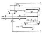
- T1, T2, T3 and T4 denote four transistors which form two push-pull arranged amplifier stages T1, T3 and T2, T4 respectively which are connected in parallel and driven in push-pull.
- the load Rec is connected between the common points C and D for the two transistors in the stages T1, T3 and T2, T4 respectively.
- the circuit is intended to be designed as a monolithic integrated circuit all the transistors T1 T4 are of npn-type. However, it is naturally possible to use other known combinations of transistors in the push-pull stages.
- the output stage is driven by a differential input stage T7, T8, the base circuits of which are connected to a signal input lNa, INb through the resistances R7, R8.
- the emitters of the differential stage are as usual connected to a constant current source Is which is schematically drawn but can consist of some transistor circuit known per se.
- the collector side in the differential amplifier T7, T8 is connected partly to the bases of the transistors T1 and T2 partly to the terminal +V of a single voltage source through two of the collectors and the emitter of transistors T6 connected as a current mirror.
- a third collector in the transistor T6 connected to the base is connected to the negative terminal pole -V through a series transistor T5 controlled by a reference voltage Vref and an emitter resistance R4 common to the transistors T3 and T4 in the output amplifier.
- the push-pull input signals to the transistors T3 and T4 are received from a voltage divider R1, R2, R3 connected between the points C and D.
- the base of the transistor T3 is connected to the common point between R2 and R3 whereas the base of the transistor T4 is connected to the common point between the resistances R1 and R2.
- the points C and D are also connected to the base circuits in the transistors T7 and T8 through the feed back resistances R5 and R6.
- the circuit operates in the following way.
- a balanced signal applied to the inputs INa and INb is amplified in the differential amplifier T7, T8 and fed in a balanced way to the base circuits in the transistors T1 and T2 in the output amplifier stage.
- the operating point for these transistors T1 and T2 is determined by the transistor T6 connected as a current mirror where two collectors supply base current to the transistors T1 and T2.
- the load Rec connected between the emitters in the transistors T1 and T2 does not carry any current in case the emitter voltages are alike.
- the bottom transistors T3, T4 receive the base current feed from the emitter circuit in the opposite top transistor T2 and T1' respectively through the resistor network R 1, R2, R3.
- An incoming signal which for example makes the transistor T1 more conducting than T2 means that also the transistor T4 becomes more conducting than T3 and a current will pass through the load Rec.
- the signal polarity is the reverse on the bases of the transistors T1 and T2 the direction of current through the load is the reverse.
- An increasing current through one of the transistors for example T3 corresponds to an identical current decrease through the transistor T4. If, however, the balance is not perfect, which is the case in integrated circuits which are not specially trimmed, a so called common mode signal will flow to the current source. If the impedance of the current source is high, which is the case when a telephone instrument amplifier sets its current supply through the telephone line, the voltage of the supply point will be modulated and there is a risk that the amplifier becomes unstable.
- the direct current sum through the resistance R4 can also vary for example with the temperature, as the whole amplifier is DC connected. A small voltage alteration in an early stage is amplified and can cause that the current through R4 is altered.
- the voltage across the resistance R4 is compared with a reference voltage Vref in the transistor T5, the collector current of which is brought to vary with the current through R4. If for example the current through R4 decreases the base current and accordingly the collector current in the transistor T5 increases. Also the emitter current in the transistor T6 increases and accordingly the two collector currents increase to the same extent. The base currents in the two transistors T1 and T2 increase and causing the current sum through the resistance R4 to be restored to the value determined by the reference voltage Vref.
- a stabilization of the differential amplification and the operating point is obtained through the symmetrical feed-back from the points C and D in the output stage to the inputs of the amplifier stage T7, T8.
Landscapes
- Engineering & Computer Science (AREA)
- Signal Processing (AREA)
- Amplifiers (AREA)
Applications Claiming Priority (2)
| Application Number | Priority Date | Filing Date | Title |
|---|---|---|---|
| SE7903931 | 1979-05-04 | ||
| SE7903931A SE417048B (sv) | 1979-05-04 | 1979-05-04 | Balanserat forsterkarutgangssteg |
Publications (2)
| Publication Number | Publication Date |
|---|---|
| EP0028229A1 EP0028229A1 (en) | 1981-05-13 |
| EP0028229B1 true EP0028229B1 (en) | 1984-10-10 |
Family
ID=20337976
Family Applications (1)
| Application Number | Title | Priority Date | Filing Date |
|---|---|---|---|
| EP80900797A Expired EP0028229B1 (en) | 1979-05-04 | 1980-04-21 | A balanced amplifier output stage |
Country Status (8)
| Country | Link |
|---|---|
| US (1) | US4450412A (da) |
| EP (1) | EP0028229B1 (da) |
| DE (1) | DE3069400D1 (da) |
| DK (1) | DK149789C (da) |
| FI (1) | FI68744C (da) |
| NO (1) | NO147167C (da) |
| SE (1) | SE417048B (da) |
| WO (1) | WO1980002488A1 (da) |
Families Citing this family (1)
| Publication number | Priority date | Publication date | Assignee | Title |
|---|---|---|---|---|
| IT1168164B (it) * | 1981-08-26 | 1987-05-20 | Ates Componenti Elettron | Stadio finale a ponte per un aplificatore audio di ricezione |
Citations (1)
| Publication number | Priority date | Publication date | Assignee | Title |
|---|---|---|---|---|
| DE2431818A1 (de) * | 1974-07-02 | 1976-01-15 | Georg Dipl Ing Figol | Nf-leistungsverstaerker |
Family Cites Families (7)
| Publication number | Priority date | Publication date | Assignee | Title |
|---|---|---|---|---|
| DE1189589B (de) * | 1963-11-12 | 1965-03-25 | Philips Nv | Transistorgegentaktschaltungsanordnung |
| US3541465A (en) * | 1966-12-28 | 1970-11-17 | Hitachi Ltd | Transistor differential amplifier circuit |
| FR1600222A (da) * | 1968-12-31 | 1970-07-20 | ||
| US3742377A (en) * | 1971-07-08 | 1973-06-26 | Nat Semiconductor Corp | Differential amplifier with means for balancing out offset terms |
| US3947778A (en) * | 1974-09-11 | 1976-03-30 | Motorola, Inc. | Differential amplifier |
| JPS5548736B2 (da) * | 1975-02-26 | 1980-12-08 | ||
| DE2807304C2 (de) * | 1978-02-21 | 1982-07-01 | Licentia Patent-Verwaltungs-Gmbh, 6000 Frankfurt | Schaltungsanordnung zum Verstärken eines in einer aus einer Teilnehmeranschlußleitung gespeisten Endstelle einer Fernmeldeanlage erzeugten Signals |
-
1979
- 1979-05-04 SE SE7903931A patent/SE417048B/sv not_active IP Right Cessation
-
1980
- 1980-04-18 FI FI801241A patent/FI68744C/sv not_active IP Right Cessation
- 1980-04-21 WO PCT/SE1980/000114 patent/WO1980002488A1/en not_active Ceased
- 1980-04-21 DE DE8080900797T patent/DE3069400D1/de not_active Expired
- 1980-04-21 EP EP80900797A patent/EP0028229B1/en not_active Expired
- 1980-04-21 US US06/227,082 patent/US4450412A/en not_active Expired - Lifetime
- 1980-12-30 NO NO803963A patent/NO147167C/no unknown
-
1981
- 1981-01-02 DK DK001481A patent/DK149789C/da active
Patent Citations (1)
| Publication number | Priority date | Publication date | Assignee | Title |
|---|---|---|---|---|
| DE2431818A1 (de) * | 1974-07-02 | 1976-01-15 | Georg Dipl Ing Figol | Nf-leistungsverstaerker |
Also Published As
| Publication number | Publication date |
|---|---|
| SE7903931L (sv) | 1980-11-05 |
| NO147167B (no) | 1982-11-01 |
| NO803963L (no) | 1980-12-30 |
| DK149789C (da) | 1987-07-13 |
| US4450412A (en) | 1984-05-22 |
| DK149789B (da) | 1986-09-29 |
| SE417048B (sv) | 1981-02-16 |
| FI68744C (fi) | 1985-10-10 |
| FI801241A7 (fi) | 1980-11-05 |
| NO147167C (no) | 1983-02-09 |
| FI68744B (fi) | 1985-06-28 |
| EP0028229A1 (en) | 1981-05-13 |
| DK1481A (da) | 1981-01-02 |
| WO1980002488A1 (en) | 1980-11-13 |
| DE3069400D1 (en) | 1984-11-15 |
Similar Documents
| Publication | Publication Date | Title |
|---|---|---|
| US4638260A (en) | Audio amplifier | |
| US4586000A (en) | Transformerless current balanced amplifier | |
| JPS62222704A (ja) | 広帯域帰還増幅器 | |
| US4723111A (en) | Amplifier arrangement | |
| US5923216A (en) | Frequency selective amplifier circuit | |
| US4460873A (en) | Active differential output direct current offset voltage compensation circuit for a differential amplifier | |
| US3629717A (en) | Circuit arrangement for stabilizing against variations in temperature and supply voltage | |
| US4442409A (en) | Push-pull non-complementary transistor amplifier | |
| US5406222A (en) | High gain transistor amplifier | |
| US4217555A (en) | Amplifier circuit arrangement with stabilized power-supply current | |
| US4357578A (en) | Complementary differential amplifier | |
| US4241314A (en) | Transistor amplifier circuits | |
| US3942129A (en) | Controlled gain amplifier | |
| KR100232242B1 (ko) | 스위칭 브릿지 증폭기 | |
| US4286226A (en) | Amplifier with electrically controlled gain, with output suitable for direct coupling | |
| US4910477A (en) | Bridge-type linear amplifier with wide dynamic range and high efficiency | |
| US5057790A (en) | High efficiency class A amplifier | |
| JPS6411166B2 (da) | ||
| JPH0712128B2 (ja) | 増幅器 | |
| US4450412A (en) | Balanced amplifier output stage | |
| US4524330A (en) | Bipolar circuit for amplifying differential signal | |
| US5166983A (en) | Mute circuit for audio amplifiers | |
| US3417339A (en) | Push-pull transistor amplifiers with transformer coupled driver | |
| JPH06276037A (ja) | オーディオ用パワーアンプ | |
| EP0913930A2 (en) | BTL amplifying circuit |
Legal Events
| Date | Code | Title | Description |
|---|---|---|---|
| PUAI | Public reference made under article 153(3) epc to a published international application that has entered the european phase |
Free format text: ORIGINAL CODE: 0009012 |
|
| 17P | Request for examination filed |
Effective date: 19801201 |
|
| AK | Designated contracting states |
Designated state(s): DE FR GB |
|
| GRAA | (expected) grant |
Free format text: ORIGINAL CODE: 0009210 |
|
| AK | Designated contracting states |
Designated state(s): DE FR GB |
|
| REF | Corresponds to: |
Ref document number: 3069400 Country of ref document: DE Date of ref document: 19841115 |
|
| ET | Fr: translation filed | ||
| PLBE | No opposition filed within time limit |
Free format text: ORIGINAL CODE: 0009261 |
|
| STAA | Information on the status of an ep patent application or granted ep patent |
Free format text: STATUS: NO OPPOSITION FILED WITHIN TIME LIMIT |
|
| 26N | No opposition filed | ||
| PGFP | Annual fee paid to national office [announced via postgrant information from national office to epo] |
Ref country code: FR Payment date: 19990331 Year of fee payment: 20 |
|
| PGFP | Annual fee paid to national office [announced via postgrant information from national office to epo] |
Ref country code: GB Payment date: 19990401 Year of fee payment: 20 |
|
| PGFP | Annual fee paid to national office [announced via postgrant information from national office to epo] |
Ref country code: DE Payment date: 19990402 Year of fee payment: 20 |
|
| PG25 | Lapsed in a contracting state [announced via postgrant information from national office to epo] |
Ref country code: GB Free format text: LAPSE BECAUSE OF EXPIRATION OF PROTECTION Effective date: 20000420 |
|
| REG | Reference to a national code |
Ref country code: GB Ref legal event code: PE20 Effective date: 20000420 |