EP0028802A1 - Elektrisch isolierendes Substrat und Verfahren zur Herstellung eines solchen Substrats - Google Patents
Elektrisch isolierendes Substrat und Verfahren zur Herstellung eines solchen Substrats Download PDFInfo
- Publication number
- EP0028802A1 EP0028802A1 EP80106791A EP80106791A EP0028802A1 EP 0028802 A1 EP0028802 A1 EP 0028802A1 EP 80106791 A EP80106791 A EP 80106791A EP 80106791 A EP80106791 A EP 80106791A EP 0028802 A1 EP0028802 A1 EP 0028802A1
- Authority
- EP
- European Patent Office
- Prior art keywords
- silicon carbide
- sintered body
- powder
- substrate
- thermal conductivity
- Prior art date
- Legal status (The legal status is an assumption and is not a legal conclusion. Google has not performed a legal analysis and makes no representation as to the accuracy of the status listed.)
- Granted
Links
Images

Classifications
-
- C—CHEMISTRY; METALLURGY
- C04—CEMENTS; CONCRETE; ARTIFICIAL STONE; CERAMICS; REFRACTORIES
- C04B—LIME, MAGNESIA; SLAG; CEMENTS; COMPOSITIONS THEREOF, e.g. MORTARS, CONCRETE OR LIKE BUILDING MATERIALS; ARTIFICIAL STONE; CERAMICS; REFRACTORIES; TREATMENT OF NATURAL STONE
- C04B35/00—Shaped ceramic products characterised by their composition; Ceramics compositions; Processing powders of inorganic compounds preparatory to the manufacturing of ceramic products
- C04B35/515—Shaped ceramic products characterised by their composition; Ceramics compositions; Processing powders of inorganic compounds preparatory to the manufacturing of ceramic products based on non-oxide ceramics
- C04B35/56—Shaped ceramic products characterised by their composition; Ceramics compositions; Processing powders of inorganic compounds preparatory to the manufacturing of ceramic products based on non-oxide ceramics based on carbides or oxycarbides
- C04B35/565—Shaped ceramic products characterised by their composition; Ceramics compositions; Processing powders of inorganic compounds preparatory to the manufacturing of ceramic products based on non-oxide ceramics based on carbides or oxycarbides based on silicon carbide
- C04B35/575—Shaped ceramic products characterised by their composition; Ceramics compositions; Processing powders of inorganic compounds preparatory to the manufacturing of ceramic products based on non-oxide ceramics based on carbides or oxycarbides based on silicon carbide obtained by pressure sintering
-
- C—CHEMISTRY; METALLURGY
- C04—CEMENTS; CONCRETE; ARTIFICIAL STONE; CERAMICS; REFRACTORIES
- C04B—LIME, MAGNESIA; SLAG; CEMENTS; COMPOSITIONS THEREOF, e.g. MORTARS, CONCRETE OR LIKE BUILDING MATERIALS; ARTIFICIAL STONE; CERAMICS; REFRACTORIES; TREATMENT OF NATURAL STONE
- C04B35/00—Shaped ceramic products characterised by their composition; Ceramics compositions; Processing powders of inorganic compounds preparatory to the manufacturing of ceramic products
- C04B35/515—Shaped ceramic products characterised by their composition; Ceramics compositions; Processing powders of inorganic compounds preparatory to the manufacturing of ceramic products based on non-oxide ceramics
- C04B35/56—Shaped ceramic products characterised by their composition; Ceramics compositions; Processing powders of inorganic compounds preparatory to the manufacturing of ceramic products based on non-oxide ceramics based on carbides or oxycarbides
- C04B35/565—Shaped ceramic products characterised by their composition; Ceramics compositions; Processing powders of inorganic compounds preparatory to the manufacturing of ceramic products based on non-oxide ceramics based on carbides or oxycarbides based on silicon carbide
-
- H—ELECTRICITY
- H01—ELECTRIC ELEMENTS
- H01B—CABLES; CONDUCTORS; INSULATORS; SELECTION OF MATERIALS FOR THEIR CONDUCTIVE, INSULATING OR DIELECTRIC PROPERTIES
- H01B3/00—Insulators or insulating bodies characterised by the insulating materials; Selection of materials for their insulating or dielectric properties
- H01B3/02—Insulators or insulating bodies characterised by the insulating materials; Selection of materials for their insulating or dielectric properties mainly consisting of inorganic substances
- H01B3/12—Insulators or insulating bodies characterised by the insulating materials; Selection of materials for their insulating or dielectric properties mainly consisting of inorganic substances ceramics
-
- H—ELECTRICITY
- H10—SEMICONDUCTOR DEVICES; ELECTRIC SOLID-STATE DEVICES NOT OTHERWISE PROVIDED FOR
- H10W—GENERIC PACKAGES, INTERCONNECTIONS, CONNECTORS OR OTHER CONSTRUCTIONAL DETAILS OF DEVICES COVERED BY CLASS H10
- H10W99/00—Subject matter not provided for in other groups of this subclass
-
- H—ELECTRICITY
- H05—ELECTRIC TECHNIQUES NOT OTHERWISE PROVIDED FOR
- H05K—PRINTED CIRCUITS; CASINGS OR CONSTRUCTIONAL DETAILS OF ELECTRIC APPARATUS; MANUFACTURE OF ASSEMBLAGES OF ELECTRICAL COMPONENTS
- H05K1/00—Printed circuits
- H05K1/02—Details
- H05K1/03—Use of materials for the substrate
- H05K1/0306—Inorganic insulating substrates, e.g. ceramic, glass
-
- H—ELECTRICITY
- H10—SEMICONDUCTOR DEVICES; ELECTRIC SOLID-STATE DEVICES NOT OTHERWISE PROVIDED FOR
- H10W—GENERIC PACKAGES, INTERCONNECTIONS, CONNECTORS OR OTHER CONSTRUCTIONAL DETAILS OF DEVICES COVERED BY CLASS H10
- H10W72/00—Interconnections or connectors in packages
- H10W72/50—Bond wires
- H10W72/531—Shapes of wire connectors
- H10W72/5363—Shapes of wire connectors the connected ends being wedge-shaped
-
- H—ELECTRICITY
- H10—SEMICONDUCTOR DEVICES; ELECTRIC SOLID-STATE DEVICES NOT OTHERWISE PROVIDED FOR
- H10W—GENERIC PACKAGES, INTERCONNECTIONS, CONNECTORS OR OTHER CONSTRUCTIONAL DETAILS OF DEVICES COVERED BY CLASS H10
- H10W72/00—Interconnections or connectors in packages
- H10W72/50—Bond wires
- H10W72/551—Materials of bond wires
- H10W72/552—Materials of bond wires comprising metals or metalloids, e.g. silver
- H10W72/5522—Materials of bond wires comprising metals or metalloids, e.g. silver comprising gold [Au]
-
- H—ELECTRICITY
- H10—SEMICONDUCTOR DEVICES; ELECTRIC SOLID-STATE DEVICES NOT OTHERWISE PROVIDED FOR
- H10W—GENERIC PACKAGES, INTERCONNECTIONS, CONNECTORS OR OTHER CONSTRUCTIONAL DETAILS OF DEVICES COVERED BY CLASS H10
- H10W72/00—Interconnections or connectors in packages
- H10W72/851—Dispositions of multiple connectors or interconnections
- H10W72/874—On different surfaces
- H10W72/884—Die-attach connectors and bond wires
-
- H—ELECTRICITY
- H10—SEMICONDUCTOR DEVICES; ELECTRIC SOLID-STATE DEVICES NOT OTHERWISE PROVIDED FOR
- H10W—GENERIC PACKAGES, INTERCONNECTIONS, CONNECTORS OR OTHER CONSTRUCTIONAL DETAILS OF DEVICES COVERED BY CLASS H10
- H10W90/00—Package configurations
- H10W90/701—Package configurations characterised by the relative positions of pads or connectors relative to package parts
- H10W90/731—Package configurations characterised by the relative positions of pads or connectors relative to package parts of die-attach connectors
- H10W90/734—Package configurations characterised by the relative positions of pads or connectors relative to package parts of die-attach connectors between a chip and a stacked insulating package substrate, interposer or RDL
-
- H—ELECTRICITY
- H10—SEMICONDUCTOR DEVICES; ELECTRIC SOLID-STATE DEVICES NOT OTHERWISE PROVIDED FOR
- H10W—GENERIC PACKAGES, INTERCONNECTIONS, CONNECTORS OR OTHER CONSTRUCTIONAL DETAILS OF DEVICES COVERED BY CLASS H10
- H10W90/00—Package configurations
- H10W90/701—Package configurations characterised by the relative positions of pads or connectors relative to package parts
- H10W90/751—Package configurations characterised by the relative positions of pads or connectors relative to package parts of bond wires
- H10W90/754—Package configurations characterised by the relative positions of pads or connectors relative to package parts of bond wires between a chip and a stacked insulating package substrate, interposer or RDL
Definitions
- This invention relates to an electrically insulating substrate having high thermal conductivity and high electric resistivity and also to a method of making such a substrate.
- insulating substrate As materials for such an insulating substrate, there has conventionally been employed an alumina sintered body. Since the alumina sintered body does not have satisfactory thermal diffusivity, however, development of an insulating substrate having higher thermal diffusivity has been requested.
- the insulating substrate for such an application must satisfy the following requirements:
- a sintered body of silicon carbide has a coefficient of thermal expansion of 3.7 ⁇ 10 -6 /°C which is smaller than the coefficient of thermal expansion of alumina, i.e., about 8 x 10 -6 /°C and is approximate to that of silicon, i.e., about 3.3 x 10 -6 /°C.
- its bending strength is at least 500 N/mm2, the value being by far higher than that of alumina, i.e., ca. 250 to 300 N/mm 2 .
- the thermal conductivity of a silicon carbide sintered body is 0.42 to 0.84 J/cm ⁇ sec ⁇ °C which is at least three times that of alumina.
- Silicon carbide is a semiconductor compound of the Group IV-IV consisting of carbon and silicon. For this reason, it has been believed difficult to obtain a high density sintered body of silicon carbide with high electrical resistivity and as a matter of fact, no such sintered body has been found to this date.
- silicon carbide is a compound having high covalent bond, it is hard and tough and is stable both in oxidation resistance and corrosion resistance even at a temperature of 1,500°C or above. Due to this strong covalent bond, however, it is a material from which a high density sintered body can not be obtained easily.
- U.S. Patent No. 4,172,109 discloses a sintered body of silicon carbide which is sintered while Be is added as the aid.
- This prior art relates to a high strength material obtained by sintering the raw powder of silicon carbide which contains 0.5 to 5 wt.% of excessive carbon.
- the sintered body thus formed has small electric resistivity and can not be used as an electrically insulating material.
- the electrically insulating substrate in accordance with the present invention is formed by adding 0.1 to 3.5 wt. % of beryllium oxide powder, calculated as beryllium, to silicon carbide powder as the principal component, pressure-molding the mixed powder and then sintering the resulting molded article at such a temperature and pressure sufficient to provide 90 % relative density.
- the aluminum, boron and free carbon components in the silicon carbide powder are restricted to at most 0.1 wt.%, at most 0.1 wt.% and at most 0.4 wt.%, respectively.
- the thermal conductivity at 25°C of the electrically insulating substrate obtained from this sintered body is at least 1.67 ⁇ J/cm sec ⁇ °C. while its electrical resistivity at 25°C is at least 10 7 ohm ⁇ cm. Further, its coefficient of heat expansion from 25°C to 300°C is up to 3.7 x 10 -6 /°C.
- the amount of beryllium in the sintered body is restricted to from 0.1 to 3.5 wt.% for the following reason. If it is below 0.1 wt.%, the electrical resistivity becomes smaller than 10 7 ohm.cm while if it exceeds 3.5 wt.%, the thermal expansion coefficient of the sintered body becomes greater than 4 x 10 -6 °C , thus rendering a critical problem when the sintered body is used as an insulating substrate especially for silicon semiconductor elements.
- BeO beryllium as BeO.
- the addition is made by mixing the Be0 powder and the silicon carbide powder. If about 0.5 to 14 wt.% of Be0 is added in this case, Be in the sintered body accounts for about 0.1 to 3.5 wt.%. However, these values vary to some extents depending upon the atmosphere and temperature during the sintering.
- the silicon carbide powder does not contain more than 0.4 wt.% of free carbon.
- the presence of free carbon in such an amount markedly reduces the electrical resistivity as one of the objects of the present invention.
- the above mentioned beryllium oxide powder and silicon carbide powder are minute powders having an average grain size of up to 10 ⁇ m, preferably up to 2 ⁇ m, and the powder is sintered by hot-pressing.
- aluminum and boron are not contained preferably in the sintered body, there is no problem if their contents are below 0.1 wt.%, respectively. If aluminum is contained in a greater amount, the electrical resistivity of the sintered body becomes below 10 7 Ohm ⁇ cm disadvantageously. If boron is contained in a greater amount, the thermal conductivity becomes smaller than 1.67 J/cm ⁇ sec ⁇ °C.
- the sintering condition of BeO-containing silicon carbide powder is also an important factor, and specifically, sintering must be carried out in a non-oxidizing atmosphere.
- a non-oxidizing atmosphere the surface of the silicon carbide powder is oxidized so that a high density sintered body cannot be obtained.
- furnace materials that can be used in an oxidizing atmosphere at a temperature of about 2,000°C are not available at present.
- the sintering temperature is from 1,850 to 2,500°C , prefer ply from 1,900 to 2,300°C. If the temperature is lower then 1,850°C , a high density sintered body cannot be obtained while at a sintering temperature higher than 2,500°C , sublimation of silicon carbide becomes so vigorous that the sintered body is excessively sintered and hence, is not changed into a compact ceramic.
- the upper limit of the pressurizing load varies with the material of dies to be employed. Generally, the dies are made of graphite and in that c ⁇ se, a pressure of up to about 700 bar may be applied.
- a high density sintered body without applying such a great pressure.
- the pressure ranges from 100 to 300 bar. If the silicon carbide powder having a sub-micron grain size is employed, a compact sintered body (relative density of 90 %) can be obtained without applying the pressure.
- the optimum sintering time can be determined in accordance with the grain size of the raw powder, the sintering temperature and the load applied during the sintering. Generally speaking, a high density sintered body can be obtained within a short sintering time if the grain size of the raw material powder is small, the sintering temperature is high and the load applied during the sintering is great.
- Beryllium oxide powder having a grain size of up to 10 ⁇ m was mixed with silicon carbide powder of an average grain size of 2 ⁇ m in an amount of 0.1 to 20 wt.%.
- the mixture was shaped into a mold at a room temperature by applying a pressure of 980 bar.
- the mold had a density of 1.60 to 1.67 g/cm 3 (50 to 52 % relative density with respect to the theoretical density of silicon carbide).
- the molded article was placed in a graphite die and was sintered by a hot press method at a reduced pressure 1.33 x 10 -3 to 0.13 Pa.
- the sintering pressure was 300 bar and the temperature was raised from room temperature to 2,000°C in the course of about two hours, was held at 2,000°C for one hour and was then left cooling by cutting off a heating power source. The pressure was. released after the temperature fell below 1,500°C.
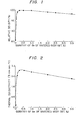
- the relationship between the properties of the silicon carbide sintered body thus produced and the Be quantity is shown in Figures 1 through 4.
- Sintered bodies were produced in the same way as in Example 1 except that the BeO quantity was changed to 3 wt.% and the atmosphere was changed to Ar gas, He gas and N 2 gas, respectively.
- the Be content in the resulting sintered bodies was 0.9 wt.%.
- the properties of each sintered body were virtually the same as those of the sintered body of Example 1 containing 1 wt.% of Be.
- Mixed powder was formed by adding 2 wt.% of BeO powder and 0.3 to 3 wt.%, based on silicon carbide, of carbon black (minute powder of a grain size of 0.1 ⁇ m or below) as an impurity to the silicon carbide powder.
- the mixed powder was hot-pressed in the same way as in Example 1, yielding a sintered body.
- various sintered bodies were produced by changing the quantity of the carbon black.
- Table 3 illustrates the relationship between the carbon black quantity and the properties of the sintered bodies. When the carbon black quantity was 0.5 wt.%, the electrical resistivity of the product became 10 6 Ohm ⁇ cm.
- Sintered bodies of silicon carbide were produced in the same way as in Example 5 except that aluminum nitride powder (minute powder of a grain size of up to 2 ⁇ m) was employed as an impurity instead of carbon black of Example 5.
- Table 4 illustrates the relationship between the aluminum quantity and the properties of each sintered body when the former was changed. It was found that when the aluminum quantity became smaller than 0.1 wt.%, the electrical resistivity of the sintered body became extremely small.
- Sintered bodies of silicon carbide were produced in the same way as in Example 5 except that boron nitride powder (minute powder of a grain size of up to 5 ⁇ m) was employed instead of the carbon black of Example 5.
- Table 5 illustrates the relationship between the boron quantity and the properties of the sintered body. It was found that when the boron content was more than 0.1 wt.%, the thermal conductivity of the sintered body was remarkably reduced.
- the silicon carbide powder was used one that was synthesized in high frequency heat plasma.
- the powder was extremely minute powder having a grain size of 2 0 nm 0.2 ⁇ m, BeO powder of an average grain size of 1 ⁇ m was added to the silicon carbide powder.
- the resulting molded article was sintered in vacuum of 1 .22 x 10 -2 Pa. Heating was made from room temperature to 2,100°C. in the course of about 2 hours, held at 2,100°C for 0.5 hour, and was thereafter left cooling by cutting off the heating power source.
- the Be content in the sintered body was about 0.4 wt.%. Table 6 illustrates the properties of the resulting sintered body.
- the sintered body was rendered compact and had high thermal conductivity, high electrical resistance and low coefficient of thermal expansion.
- Coefficient of thermal expansion is a mean value of room temperature to 300°C.
- a semiconductor power module was produced using the silicon carbide sintered body of 0.5 wt.% beryllium content obtained in Example 1.
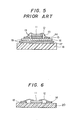
- Figure 5 shows the section of a semiconductor power module assembly of the prior art.
- An organic insulating material 15 is interposed for insulation between a Cu conductor 14 and a Cu heat sink 16 while an aluminum substrate 17 is interposed for insulation between the heat sink 16 and a Cu metal support 18.
- a spacer 13 is interposed in order to mitigate strain due to the difference of thermal expansion coefficients between a silicon element 11 and the Cu heat sink 16.
- Reference numeral 12 denotes an aluminum lead wire while reference numeral 19 denotes a solder.
- FIG. 6 is a sectional view of the module assembly using the insulating substrate in accordance with the present invention.
- the substrate 20 of the present invention has an extremely simple construction in which the substrate is directly brazed to the silicon element 11 via the solder 19.
- the abovementioned semiconductor device was held at -60°C for 30 minutes, then at room temperature for 5 minutes and thereafter heated to 125°C and held at that temperature for 30 minutes.
- This heat cycle was applied 20 times to the semiconductor device of the prior art shown in Figure 5, crack occurred on the alumina substrate and soldered positions peeled off.
- the same heat cycle was applied 150 times to the semiconductor device of the present invention shown in Figure 6, no abnormality was observed.
- a sintered body was hot-pressed in the same way as in Example 1 except that no additive was added.
- the properties of the resulting sintered body are shown in Table 7. Since the sintered body was not rendered compact, all of the thermal conductivity, electrical resistivity and mechanical strength were low.
- Example 2 Two percents by weight (2 wt.%) of aluminum oxide was added as an additive to the silicon carbide powder.
- the mixed powder was molded and hot-pressed in the same way as in Example 1, yielding a sintered body.
- the properties of the sintered body are shown in Table 8. Though the mechanical strength was high, the thermal conductivity as well as electrical resistivity were low. Similar properties were obtained when aluminum carbide, aluminum nitride and aluminum phosphate were respectively added as the additive to the silicon carbide powder.
- the silicon carbide sintered body in accordance with the present invention is characterized by its high compactness, high thermal conductivity, high electrical resistivity and low coefficient of thermal expansion. Accordingly, the sintered body of the invention is excellent as the aforementioned electrically insulating substrate. Further, it can be used suitably as a member for which heat resistance and oxidation resistance are requisites or as a member for which high strength at high temperature is required.
Landscapes
- Chemical & Material Sciences (AREA)
- Engineering & Computer Science (AREA)
- Ceramic Engineering (AREA)
- Manufacturing & Machinery (AREA)
- Materials Engineering (AREA)
- Structural Engineering (AREA)
- Organic Chemistry (AREA)
- Inorganic Chemistry (AREA)
- Ceramic Products (AREA)
Applications Claiming Priority (4)
| Application Number | Priority Date | Filing Date | Title |
|---|---|---|---|
| JP142059/79 | 1979-11-05 | ||
| JP54142059A JPS5831755B2 (ja) | 1979-11-05 | 1979-11-05 | 電気絶縁用基体 |
| JP75601/80 | 1980-06-06 | ||
| JP55075601A JPS5815953B2 (ja) | 1980-06-06 | 1980-06-06 | 電気的装置用基板 |
Publications (2)
| Publication Number | Publication Date |
|---|---|
| EP0028802A1 true EP0028802A1 (de) | 1981-05-20 |
| EP0028802B1 EP0028802B1 (de) | 1983-08-17 |
Family
ID=26416743
Family Applications (1)
| Application Number | Title | Priority Date | Filing Date |
|---|---|---|---|
| EP80106791A Expired EP0028802B1 (de) | 1979-11-05 | 1980-11-04 | Elektrisch isolierendes Substrat und Verfahren zur Herstellung eines solchen Substrats |
Country Status (3)
| Country | Link |
|---|---|
| US (2) | US4370421A (de) |
| EP (1) | EP0028802B1 (de) |
| DE (1) | DE3064598D1 (de) |
Cited By (15)
| Publication number | Priority date | Publication date | Assignee | Title |
|---|---|---|---|---|
| EP0081365A1 (de) * | 1981-12-07 | 1983-06-15 | Hitachi, Ltd. | Elektrisch isolierender gesinterter Formkörper aus Siliziumkarbid |
| EP0107821A1 (de) * | 1982-10-06 | 1984-05-09 | Hitachi, Ltd. | Verfahren zur Herstellung eines Siliciumcarbidkörpers |
| FR2536209A1 (fr) * | 1982-11-12 | 1984-05-18 | Hitachi Ltd | Substrat de cablage, procede de fabrication de ce substrat et dispositif a semi-conducteurs utilisant un tel substrat |
| EP0064264A3 (en) * | 1981-04-30 | 1984-06-13 | Hitachi, Ltd. | Silicon carbide powder mixture and process for producing sintered bodies therefrom |
| EP0064386A3 (en) * | 1981-04-30 | 1984-07-04 | Hitachi, Ltd. | Silicon carbide electrical insulator material of low dielectric constant and manufacturing method therefor |
| DE3401984A1 (de) * | 1983-01-21 | 1984-07-26 | Hitachi, Ltd., Tokio/Tokyo | Verkapselte integrierte schaltung |
| EP0097058A3 (en) * | 1982-06-16 | 1984-10-03 | Hitachi, Ltd. | Sic sintered body having metallized layer and production method therefor |
| EP0081992A3 (de) * | 1981-12-11 | 1984-11-14 | Hitachi, Ltd. | Halbleiteranordnung mit keramischer Packung |
| US4486543A (en) * | 1980-11-24 | 1984-12-04 | Feldmuhle Aktiengesellschaft | Polycrystalline shaped body of silicon carbide and method for its production |
| EP0078684A3 (en) * | 1981-10-30 | 1985-05-22 | Fujitsu Limited | A semiconductor device having a leadless chip carrier |
| US4651192A (en) * | 1981-12-04 | 1987-03-17 | Hitachi, Ltd. | Ceramic packaged semiconductor device |
| EP0251218A3 (de) * | 1986-06-26 | 1988-03-23 | Elektroschmelzwerk Kempten GmbH | Elektrisch isolierende Substratwerkstoffe aus polykristallinem Siliciumcarbid und Verfahren zu ihrer Herstellung durch isostatisches Heisspressen |
| US4760312A (en) * | 1982-08-04 | 1988-07-26 | Ngk Spark Plug Co., Ltd. | Dense silicon carbide microwave absorber for electron linear accelerator |
| EP0626358A3 (de) * | 1993-05-27 | 1995-06-28 | Kai Yin Dr Chia | Elektrisch leitende, hochfeste und dichte Keramik. |
| EP0665196A1 (de) * | 1994-01-27 | 1995-08-02 | CERAMIQUES & COMPOSITES S.A. | Verfahren zur Herstellung von keramischen Siliciumcarbidmaterialien, im wesentlichen in der alpha-form und die insbesondere nach diesem verfahren erhaltenen keramischen materialien |
Families Citing this family (20)
| Publication number | Priority date | Publication date | Assignee | Title |
|---|---|---|---|---|
| DE3064598D1 (en) * | 1979-11-05 | 1983-09-22 | Hitachi Ltd | Electrically insulating substrate and a method of making such a substrate |
| JPS59126665A (ja) * | 1983-01-10 | 1984-07-21 | Hitachi Ltd | 厚膜混成集積回路 |
| US4672421A (en) * | 1984-04-02 | 1987-06-09 | Motorola, Inc. | Semiconductor packaging and method |
| US4650922A (en) * | 1985-03-11 | 1987-03-17 | Texas Instruments Incorporated | Thermally matched mounting substrate |
| US4729010A (en) * | 1985-08-05 | 1988-03-01 | Hitachi, Ltd. | Integrated circuit package with low-thermal expansion lead pieces |
| JPS6271271A (ja) * | 1985-09-24 | 1987-04-01 | Sharp Corp | 炭化珪素半導体の電極構造 |
| US4701427A (en) * | 1985-10-17 | 1987-10-20 | Stemcor Corporation | Sintered silicon carbide ceramic body of high electrical resistivity |
| US4987103A (en) * | 1986-04-09 | 1991-01-22 | Nippon Pillar Packing Co., Ltd. | Slider composed of a high-density silicon carbide sintered compact |
| US4796077A (en) * | 1986-08-13 | 1989-01-03 | Hitachi, Ltd. | Electrical insulating, sintered aluminum nitride body having a high thermal conductivity and process for preparing the same |
| EP0326077B1 (de) * | 1988-01-25 | 1995-04-12 | Kabushiki Kaisha Toshiba | Schaltungsplatte |
| JPH02263445A (ja) * | 1988-12-23 | 1990-10-26 | Toshiba Corp | 窒化アルミニウム基板およびそれを用いた半導体装置 |
| US5094985A (en) * | 1989-01-30 | 1992-03-10 | Kazunori Kijima Kyoto | Sintered silicon carbide body with high thermal conductivity and process of producing the same |
| US5093039A (en) * | 1989-01-30 | 1992-03-03 | Kazunori Kijima | Highly pure sintered carbide with high electric conductivity and process of producing the same |
| US4994903A (en) * | 1989-12-18 | 1991-02-19 | Texas Instruments Incorporated | Circuit substrate and circuit using the substrate |
| JPH0798460A (ja) * | 1992-10-21 | 1995-04-11 | Seiko Instr Inc | 半導体装置及び光弁装置 |
| DE19732439B4 (de) * | 1997-07-28 | 2006-01-19 | Infineon Technologies Ag | Leistungshalbleiterbauelement auf Kühlkörper |
| EP1174400A4 (de) * | 1999-11-30 | 2006-02-01 | Ibiden Co Ltd | Hochdichtgesintertes, poröses siliziumkarbid und sliziumkarbid-metal-komposit zur verwendung in tischen von halbleiterscheiben-poliermaschinen |
| DE102009022877B4 (de) * | 2009-04-29 | 2014-12-24 | Rogers Germany Gmbh | Gekühlte elektrische Baueinheit |
| US10600635B2 (en) | 2017-04-20 | 2020-03-24 | Elyakim Kassel | Method and apparatus for a semiconductor-on-higher thermal conductive multi-layer composite wafer |
| CN116178022A (zh) * | 2022-12-19 | 2023-05-30 | 先进能源科学与技术广东省实验室 | 一种高致密度、高导热的碳化硅-氧化铍复合陶瓷及其制备方法 |
Citations (5)
| Publication number | Priority date | Publication date | Assignee | Title |
|---|---|---|---|---|
| GB956911A (en) * | 1961-06-01 | 1964-04-29 | Nat Beryllia Corp | Beryllia silicon carbide ceramic bodies |
| US4023975A (en) * | 1975-11-17 | 1977-05-17 | General Electric Company | Hot pressed silicon carbide containing beryllium carbide |
| US4105456A (en) * | 1976-02-04 | 1978-08-08 | Nippon Telegraph & Telephone Public Corporation | Ceramic material of low thermal expansion coefficient and method of manufacturing the same |
| US4172109A (en) * | 1976-11-26 | 1979-10-23 | The Carborundum Company | Pressureless sintering beryllium containing silicon carbide powder composition |
| GB2031027A (en) * | 1978-09-04 | 1980-04-16 | Hitachi Ltd | Sintered silicon carbide product and process for producing the same |
Family Cites Families (7)
| Publication number | Priority date | Publication date | Assignee | Title |
|---|---|---|---|---|
| US3205080A (en) * | 1964-10-19 | 1965-09-07 | Nat Beryllia Corp | Beryllia-silicon carbide ceramic bodies |
| US3993602A (en) * | 1975-11-17 | 1976-11-23 | General Electric Company | Polycrystalline silicon carbide with increased conductivity |
| US4123286A (en) * | 1976-12-27 | 1978-10-31 | The Carborundum Company | Silicon carbide powder compositions |
| US4141726A (en) * | 1977-04-04 | 1979-02-27 | The Research Institute For Iron, Steel And Other Metals Of The Tohoku University | Method for producing composite materials consisting of continuous silicon carbide fibers and beryllium |
| JPS55143042A (en) * | 1979-04-25 | 1980-11-08 | Hitachi Ltd | Semiconductor device |
| JPS5615047A (en) * | 1979-07-19 | 1981-02-13 | Hitachi Ltd | Semiconductor device |
| DE3064598D1 (en) * | 1979-11-05 | 1983-09-22 | Hitachi Ltd | Electrically insulating substrate and a method of making such a substrate |
-
1980
- 1980-11-04 DE DE8080106791T patent/DE3064598D1/de not_active Expired
- 1980-11-04 EP EP80106791A patent/EP0028802B1/de not_active Expired
- 1980-11-05 US US06/203,554 patent/US4370421A/en not_active Expired - Lifetime
-
1982
- 1982-12-16 US US06/450,566 patent/US4571610A/en not_active Expired - Lifetime
Patent Citations (5)
| Publication number | Priority date | Publication date | Assignee | Title |
|---|---|---|---|---|
| GB956911A (en) * | 1961-06-01 | 1964-04-29 | Nat Beryllia Corp | Beryllia silicon carbide ceramic bodies |
| US4023975A (en) * | 1975-11-17 | 1977-05-17 | General Electric Company | Hot pressed silicon carbide containing beryllium carbide |
| US4105456A (en) * | 1976-02-04 | 1978-08-08 | Nippon Telegraph & Telephone Public Corporation | Ceramic material of low thermal expansion coefficient and method of manufacturing the same |
| US4172109A (en) * | 1976-11-26 | 1979-10-23 | The Carborundum Company | Pressureless sintering beryllium containing silicon carbide powder composition |
| GB2031027A (en) * | 1978-09-04 | 1980-04-16 | Hitachi Ltd | Sintered silicon carbide product and process for producing the same |
Non-Patent Citations (2)
| Title |
|---|
| IBM TECHNICAL DISCLOSURE BULLETIN, Vol. 11, No. 11, April 1969, New York, USA A.J. BLODGETT: "Composite structures for modifying thermal coefficient of expansion", page 1559. * Page 1559 * * |
| SOLID STATE TECHNOLOGY, Vol. 20, No. 1, January 1977, Washington, US P.L. FLEISCHNER: "Beryllia Ceramics in Microelectronic Applications", pages 25-30. * Pages 25-27; figures 1-7 * * |
Cited By (19)
| Publication number | Priority date | Publication date | Assignee | Title |
|---|---|---|---|---|
| US4486543A (en) * | 1980-11-24 | 1984-12-04 | Feldmuhle Aktiengesellschaft | Polycrystalline shaped body of silicon carbide and method for its production |
| EP0064386A3 (en) * | 1981-04-30 | 1984-07-04 | Hitachi, Ltd. | Silicon carbide electrical insulator material of low dielectric constant and manufacturing method therefor |
| EP0064264A3 (en) * | 1981-04-30 | 1984-06-13 | Hitachi, Ltd. | Silicon carbide powder mixture and process for producing sintered bodies therefrom |
| US4910584A (en) * | 1981-10-30 | 1990-03-20 | Fujitsu Limited | Semiconductor device |
| EP0078684A3 (en) * | 1981-10-30 | 1985-05-22 | Fujitsu Limited | A semiconductor device having a leadless chip carrier |
| US4651192A (en) * | 1981-12-04 | 1987-03-17 | Hitachi, Ltd. | Ceramic packaged semiconductor device |
| US4561010A (en) * | 1981-12-07 | 1985-12-24 | Hitachi, Ltd. | Electrically insulating silicon carbide sintered body |
| EP0081365A1 (de) * | 1981-12-07 | 1983-06-15 | Hitachi, Ltd. | Elektrisch isolierender gesinterter Formkörper aus Siliziumkarbid |
| US4517584A (en) * | 1981-12-11 | 1985-05-14 | Hitachi, Ltd. | Ceramic packaged semiconductor device |
| EP0081992A3 (de) * | 1981-12-11 | 1984-11-14 | Hitachi, Ltd. | Halbleiteranordnung mit keramischer Packung |
| EP0097058A3 (en) * | 1982-06-16 | 1984-10-03 | Hitachi, Ltd. | Sic sintered body having metallized layer and production method therefor |
| US4760312A (en) * | 1982-08-04 | 1988-07-26 | Ngk Spark Plug Co., Ltd. | Dense silicon carbide microwave absorber for electron linear accelerator |
| US4561891A (en) * | 1982-10-06 | 1985-12-31 | Hitachi, Ltd. | Powdery silicon carbide composition for sintering |
| EP0107821A1 (de) * | 1982-10-06 | 1984-05-09 | Hitachi, Ltd. | Verfahren zur Herstellung eines Siliciumcarbidkörpers |
| FR2536209A1 (fr) * | 1982-11-12 | 1984-05-18 | Hitachi Ltd | Substrat de cablage, procede de fabrication de ce substrat et dispositif a semi-conducteurs utilisant un tel substrat |
| DE3401984A1 (de) * | 1983-01-21 | 1984-07-26 | Hitachi, Ltd., Tokio/Tokyo | Verkapselte integrierte schaltung |
| EP0251218A3 (de) * | 1986-06-26 | 1988-03-23 | Elektroschmelzwerk Kempten GmbH | Elektrisch isolierende Substratwerkstoffe aus polykristallinem Siliciumcarbid und Verfahren zu ihrer Herstellung durch isostatisches Heisspressen |
| EP0626358A3 (de) * | 1993-05-27 | 1995-06-28 | Kai Yin Dr Chia | Elektrisch leitende, hochfeste und dichte Keramik. |
| EP0665196A1 (de) * | 1994-01-27 | 1995-08-02 | CERAMIQUES & COMPOSITES S.A. | Verfahren zur Herstellung von keramischen Siliciumcarbidmaterialien, im wesentlichen in der alpha-form und die insbesondere nach diesem verfahren erhaltenen keramischen materialien |
Also Published As
| Publication number | Publication date |
|---|---|
| EP0028802B1 (de) | 1983-08-17 |
| DE3064598D1 (en) | 1983-09-22 |
| US4370421A (en) | 1983-01-25 |
| US4571610A (en) | 1986-02-18 |
Similar Documents
| Publication | Publication Date | Title |
|---|---|---|
| EP0028802B1 (de) | Elektrisch isolierendes Substrat und Verfahren zur Herstellung eines solchen Substrats | |
| US4540673A (en) | Sintered aluminum nitride and semi-conductor device using the same | |
| US4591537A (en) | Combination of AlN-Y2 O3 heat conductive ceramic substrate and electronic component | |
| US5409864A (en) | Substrate for semiconductor apparatus | |
| Kuramoto et al. | Translucent A1N ceramic substrate | |
| EP0330848B1 (de) | Wärmeleitender, gesinterte Aluminiumnitridkörper und sein Herstellungsverfahren | |
| US4788627A (en) | Heat sink device using composite metal alloy | |
| US6737168B1 (en) | Composite material and semiconductor device using the same | |
| EP0499865B1 (de) | Glas-Aluminiumnitrid Verbundwerkstoff | |
| JP2000303126A (ja) | ダイヤモンド−アルミニウム系複合材料およびその製造方法 | |
| EP0064386B1 (de) | Elektrisch isolierendes Material mit niedriger Dielektrizitätskonstante aus Siliciumkarbid und Verfahren zu seiner Herstellung | |
| US5409869A (en) | Aluminum nitride sintered body, method for manufacturing the same, and ceramic circuit board | |
| JPS61270262A (ja) | 高熱伝導性窒化アルミニウム焼結体 | |
| EP0393524A2 (de) | Verfahren zur Herstellung eines Sinterkörpers aus Aluminiumnitrid | |
| EP0064264B1 (de) | Siliciumkarbidpulvermischung und Verfahren zur Herstellung von Sinterkörpern aus dieser Pulvermischung | |
| JPH1179872A (ja) | メタライズ窒化ケイ素系セラミックス、その製造方法及びその製造に用いるメタライズ組成物 | |
| JPH06216481A (ja) | セラミックス銅回路基板 | |
| JPH0636473B2 (ja) | 多層セラミツク基板 | |
| JPS5815953B2 (ja) | 電気的装置用基板 | |
| JPH0995745A (ja) | 低熱膨張・高熱伝導性銅複合材料及びその製造方法 | |
| JPS6236988B2 (de) | ||
| JPS61281074A (ja) | メタライズ用高熱伝導性窒化アルミニウム焼結体 | |
| JP2003277875A (ja) | 銅−炭化タングステン複合材料 | |
| JPS61130438A (ja) | 半導体装置用材料の製造方法 | |
| JPH06183864A (ja) | 窒化けい素メタライズ基板 |
Legal Events
| Date | Code | Title | Description |
|---|---|---|---|
| PUAI | Public reference made under article 153(3) epc to a published international application that has entered the european phase |
Free format text: ORIGINAL CODE: 0009012 |
|
| AK | Designated contracting states |
Designated state(s): DE FR GB NL |
|
| 17P | Request for examination filed |
Effective date: 19811015 |
|
| GRAA | (expected) grant |
Free format text: ORIGINAL CODE: 0009210 |
|
| AK | Designated contracting states |
Designated state(s): DE FR GB NL |
|
| REF | Corresponds to: |
Ref document number: 3064598 Country of ref document: DE Date of ref document: 19830922 |
|
| ET | Fr: translation filed | ||
| PLBE | No opposition filed within time limit |
Free format text: ORIGINAL CODE: 0009261 |
|
| STAA | Information on the status of an ep patent application or granted ep patent |
Free format text: STATUS: NO OPPOSITION FILED WITHIN TIME LIMIT |
|
| 26N | No opposition filed | ||
| PGFP | Annual fee paid to national office [announced via postgrant information from national office to epo] |
Ref country code: FR Payment date: 19991022 Year of fee payment: 20 |
|
| PGFP | Annual fee paid to national office [announced via postgrant information from national office to epo] |
Ref country code: GB Payment date: 19991025 Year of fee payment: 20 |
|
| PGFP | Annual fee paid to national office [announced via postgrant information from national office to epo] |
Ref country code: NL Payment date: 19991027 Year of fee payment: 20 |
|
| PGFP | Annual fee paid to national office [announced via postgrant information from national office to epo] |
Ref country code: DE Payment date: 19991231 Year of fee payment: 20 |
|
| PG25 | Lapsed in a contracting state [announced via postgrant information from national office to epo] |
Ref country code: GB Free format text: LAPSE BECAUSE OF EXPIRATION OF PROTECTION Effective date: 20001103 |
|
| PG25 | Lapsed in a contracting state [announced via postgrant information from national office to epo] |
Ref country code: NL Free format text: LAPSE BECAUSE OF EXPIRATION OF PROTECTION Effective date: 20001104 |
|
| REG | Reference to a national code |
Ref country code: GB Ref legal event code: PE20 Effective date: 20001103 |
|
| NLV7 | Nl: ceased due to reaching the maximum lifetime of a patent |
Effective date: 20001104 |