EP0029574B1 - Analog-Techniken verwendende Wahltastatur für automatischen Fernsprechapparat - Google Patents
Analog-Techniken verwendende Wahltastatur für automatischen Fernsprechapparat Download PDFInfo
- Publication number
- EP0029574B1 EP0029574B1 EP80107158A EP80107158A EP0029574B1 EP 0029574 B1 EP0029574 B1 EP 0029574B1 EP 80107158 A EP80107158 A EP 80107158A EP 80107158 A EP80107158 A EP 80107158A EP 0029574 B1 EP0029574 B1 EP 0029574B1
- Authority
- EP
- European Patent Office
- Prior art keywords
- voltage
- key
- comparator
- columns
- oscillator
- Prior art date
- Legal status (The legal status is an assumption and is not a legal conclusion. Google has not performed a legal analysis and makes no representation as to the accuracy of the status listed.)
- Expired
Links
Images

Classifications
-
- H—ELECTRICITY
- H04—ELECTRIC COMMUNICATION TECHNIQUE
- H04M—TELEPHONIC COMMUNICATION
- H04M1/00—Substation equipment, e.g. for use by subscribers
- H04M1/26—Devices for calling a subscriber
- H04M1/30—Devices which can set up and transmit only one digit at a time
- H04M1/50—Devices which can set up and transmit only one digit at a time by generating or selecting currents of predetermined frequencies or combinations of frequencies
Definitions
- the present invention relates to an automatic telephone set call keypad and in particular a call keypad using a composite signal, the sum of two sinusoidal signals of different voice frequencies used to locate the called subscriber.
- the keyboard according to the present invention overcomes this drawback.
- the process employed allows inhibition of the oscillator when keys are pressed at the same time.
- the present invention relates to an automatic telephone set call keyboard comprising a keyboard comprising a set of conductive lines and columns and at least ten keys situated at the point of intersection of said lines and columns and each capable of bringing a contact column among four with one line among four whose columns are supplied through a voltage regulator having a low impedance output and a grounded Graetz bridge supplying said regulator according to one of its pairs of terminals , the telephone line supplying said bridge along the other of its two pairs of terminals and comprising upstream of said bridge the ringing of the device and downstream of the microphone and earphone circuits, each of said lines comprising at one of its ends a transistor switch able to connect to the ground a corresponding resistor of a double oscillator emitting one of the four lower frequencies FI and each of said columns comprising at the opposite end of said voltage regulator a transistor switch able to connect to the low impedance of said regulator a corresponding resistance of said double oscillator further emitting one of the four upper frequencies FS, the emission of the group of two
- FIG. 1 represents a diagram of the electrical and electronic principle of an automatic telephone set with a call device according to the invention.
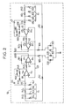
- Figure 2 shows a block diagram of the double oscillator of the call keyboard used in this device.
- FIG. 1 we see a telephone line with two wires L, and L 2 .
- Terminals L, and L 2 can be worn indifferently to the positive or negative polarity for supplying the telephone set.
- the line L, L 2 trans also puts the ringing alternating current, the ringing of the station being represented by S with the capacitor C 1 and the resistor R 1 as well as the conversation currents produced by the microphone M in parallel on the primary of a transformer T and received by the earphone E in parallel on the secondary of the transformer T.
- the contacts k 1 and k 2 are implemented by placing the telephone handset. The contacts are open in the standby position when the handset is hung up and closed in the off-hook or conversation position.
- a potentiometer P adjusts the line current.
- the invention consists in adapting a call keyboard with keys generating a frequency modulation of the line current by connecting it to points 10, 20, 30 and 40 in place of the old dial.
- a Graetz bridge D3, D4, D5, D6 whose output terminal between D3 and D5 is at a positive potential whatever the connection and therefore the polarity of the wires L 1 , L 2 of the line.
- This potential is regulated by a voltage regulator consisting of a transistor Q9, the resistor R3 and the Zener diode D7.
- the emitter of transistor Q9 delivers a regulated voltage at low impedance to the various organs of the call keypad.
- This voltage is applied on the one hand to resistors R16 to R19 placed at the ends of the four columns of a switching matrix implemented by reinforcement of its 16 keys comprising in particular the numbers 1 to 9 and 0 and on the other hand to emitters of the PNP transistors Q5 to Q8 arranged as well as the resistors R20 to R23 at the other ends of the four columns.
- the lines of the switching matrix comprise at one of their ends NPN transistors Q1 to Q4 with their resistance bridges R4 to R11. The emitters of the transistors Q1 to Q4 are connected to ground. The other ends of the lines terminate through resistors R12 to R15 and diodes D8 to D11 at a common point G connected to ground by the resistor R24 '.
- the regulated low impedance voltage from transistor Q9 is divided on the one hand by a bridge R24-R25 so as to establish a reference X to the inverting input (-) of a comparator Z 1 , the non-inverting input ( +) of said comparator Z i being connected to point G, and on the other hand, by a bridge R26-R27 so as to establish a reference Y to the inverting input (-) of a comparator Z 2 , the input not inverting (+) of said comparator Z 2 being also connected to point G.
- the bridges R24-R25 and R26-R27 are thus proportioned that the reference potential Y is greater than the reference potential X.
- the respective outputs of the comparators Z i and Z 2 are designated A and B; A is applied to the positive supply V + of a double oscillator 50 of the lower frequencies FI and higher FS controlled on switching of the transistors Q1 to Q4 and Q5 to Q8; B is applied to the negative supply V-of the double oscillator 50.
- a divider bridge R30, R31 On the outputs A and B is arranged a divider bridge R30, R31 whose midpoint providing a reference between the voltages of A and B is applied to the + of a linear amplifier Z 3 looped on the - with a gain equal to a unit.
- the output of the amplifier Z 3 decoupled by the capacitors C3 and C4 is applied to the double oscillator 50 in order to supply the latter with a low impedance voltage between V + and V - .
- the double oscillator 50 has two outputs delivering two sinusoidal frequency signals on two resistors R36 and R37 connected to the bottom of the transistor Q13 serving as frequency mixer and generator of mixed frequencies modulating the line current by the double link with the bridge.
- Graetz on the one hand between the collector of Q13 with the point common to D3 and D5 and on the other hand through the resistor R38 connected to ground and communicating with the point common to D4 and D6.
- a comparator Z4 receives on its inverting input (-) the voltage coming from A and on its non-inverting input (+) a reference taken between resistors R28 and R29 arranged between the regulated voltage of Q9 and the ground. An output C of comparator Z4 is brought to a positive potential when A is negative and to a negative potential when A is positive. These results are a function of the respective values of R28 and R29 and of the values of the bridge R24-R25. These outputs A and C are connected to the inputs of a double switch respectively the transistors Q12-Q11 and the transistor Q10.
- the transistors Q10 and Q11 are connected in series with the diodes D12 and D13 and allow the current to flow in both directions according to the collector-emitter direction when they are saturated.
- the resistors R32-R33 associated with the base of the transistor Q10 polarize the latter so that when the output C is negative the transistor Q10 is blocked and when the output C is positive the transistor Q10 is saturated.
- the set of transistors Q12-Q1 1 and the resistors R34 and R35 is mounted in such a way that when Q12 is saturated 011 is blocked and vice versa. It follows that the negative A output causes saturation of Q11 and A positive causes the blocking of 011.
- the double switch is placed between terminals 20 and 10. In parallel on the double switch is possibly a resistor R40, allowing the listening dosage while dialing numbers.
- the operating principle of the keyboard is as follows.
- the key 5 is pressed. At the crossing of the line and the column of key 5 a contact is established between the column and the line.
- the supply current supplied by the transistor Q9 crosses on the one hand the resistor R17 and on the other hand the resistor R21 thus creating a potential difference between the emitter and the base of the transistor Q6 since the column in contact with the line is grounded by diode D9 and by resistors R13 and R24.
- the transistor Q6 is therefore saturated which makes it possible to bring to the low impedance of the transistor Q9 the end of one of the positions FS controlling the double oscillator 50.
- the voltage of positive A applied to the V + of the double oscillator 50 and the negative voltage of B applied to the V- of the double oscillator 50 are in accordance with the normal supply thereof.
- the two frequencies generated by the double oscillator are mixed across the resistors R36 and R37 by the current generator 013-R38.
- the multi-frequency current thus created in the collector of Q13 modulates the line current by bypass from 40-D3-Q13-R38-mass-D4-10-P and return to L1.
- the double switch Q10-Q11 is blocked. Indeed, the output A is positive and the saturated transistor Q12 causes the blocking of the transistor 011. Furthermore, the output C is at negative potential and the transistor Q10 is blocked.
- the two frequencies FI and FS of the code are the only ones transmitted to dial the number.
- the double oscillator 50 It is made in integrated circuit thin-film hybrid built around a plate of quadruple operational amplifiers 60, 61, 62, 63.
- the differential amplifiers 60 and 63 are identical and are used respectively with resistors R41 to R50 associated with capacitors C4, C5 and resistors R51 to R60 associated with capacitors C6, C7 to produce two active filters with multiple feedback.
- Second order transfer functions have one of the lower frequencies FI and one of the higher frequencies FS as poles and can be modified by switching resistors R44 to R47 to ground and R54 to R57 at low impedance food.
- the IF frequencies are 697 Hz, 770 Hz, 852 Hz, 941 Hz.
- the FS frequencies are 1209 Hz, 1336 Hz, 1477 Hz, 1633 Hz.
- the role of the linear amplifiers 61 and 62 is to ensure a different output gain for each of them, the amplifier 62 having a gain greater than the amplifier 61 for the purpose of pre-emphasizing the higher frequencies. They also have the role of ensuring the phase inversion necessary to operate all of the amplifiers 60-61 and 62-63 in oscillators.
- a double clipping in order to stabilize the level of the signals re-injected by the resistors R41 and R51 is carried out by means of the diodes D20 to D23.
- the + inputs of the differential amplifiers 60-61-62-63 receive their voltage from Z3, the intermediate voltage between V + and V- necessary to achieve the reference voltage. Its value is positioned so as to minimize the consumption of the line supply without distorting the two transmission frequencies.
- the supply voltages of the amplifiers 60-61-62-63 are V + and V- supplied by the outputs A and B and make it possible to control the start-up of the double oscillator 50.
- the outputs of the double oscillator 50 are connected to the resistors R36 and R37.
- the call keypad according to the invention makes it possible, by analog electronic means, to perform the various functions required by this type of device, the keypad of which is interchangeable with a conventional telephone set without requiring neither equipment external to the station nor separate power supply.
- the applications are in the field of telephone telecommunications.
Landscapes
- Engineering & Computer Science (AREA)
- Signal Processing (AREA)
- Devices For Supply Of Signal Current (AREA)
- Telephone Set Structure (AREA)
Claims (1)
- Wahltastatur eines automatischen Fernsprechapparatus mit einer Tastatur, die eine Einheit aus Zeilenleitern und Spaltenleitern und mindestens zehn Tasten aufweist, die sich am Kreuzungspunkt dieser Zeilen und Spalten befinden und jede dazu in der Lage ist, eine von vier Spalten mit einer von vier Zeilen in Verbindung zu setzen, wobei die Spalten über einen Spannungsregler (Q9, R3, D7), der einen Ausgang mit niedriger Impedanz besitzt, und über eine Graetz-Brücke (D3, D4, D5, D6) versorgt werden, die mit Masse verbunden ist und den Regler über eines ihrer Klemmenpaare versorgt, während die Telephonleitung (Lj, L2), die Brücke über deren zweites Klemmenpaar vorsorgt und vor dieser Brücke (D3, D4, D5, D6) das Läutwerk (S) des Apparats und hinter ihr die Mikrophon- (M) und Höhrerschaltkreise (E) aufweist, wobei jede der Zeilen an einem ihrer Enden einen Transistorschalter (Q1, Q2, Q3, Q4) aufweist, der je einen Widerstand eines doppelten Oszillators (50), der eine der vier niedrigeren Frequenzen FI aussendet, an Masse legen kann, und jede der Spalten am diesem Spannungsregler (Q9, R3, D7) entgegengesetzten Ende einen Transistorschalter (Q5, Q6, Q7, Q8) aufweist, der an die niedrige Impedanz dieses Reglers (Q9, R3, D7) je einen Widerstand des doppelten Oszillators (50), der außerdem eine der vier höheren Frequenzen FS aussendet, anschließen kann, wobei die Aussendung der Gruppe der zwei Frequenzen, der niedrigeren FI und der höheren FS, nur möglich wird durch den Kontakt der Taste (1, 2, 3, 4, 5, 6, 7, 8, 9, 0) dadurch gekennzeichnet, daß die anderen Enden der Zeilen mit den nicht invertierenden Eingängen + eines ersten und eines zweiten Komparators (Z1, Z2) in Parallelschaltung verbunden sind, dem invertierende Eingänge - je mit dem Ausgang eines Spannungsteilers (R24, R25) bzw. (R26, R27) verbunden sind, die je vom niederohmigen Ausgang des Spannungsreglers (Q9, R3, D7) vorsorgt werden und deren jeweilige Ausgänge die Vorsorgung mit positiver und negativer Spannung des doppelten Oszillators (50) nur dann bewirken, wenn eine einzige Taste (1,...0) gedrückt ist, wobei sowohl der erste als auch der zweite Komparator (Z1, Z2) eine negative Spannung liefert, die den doppelten Oszillator (50) blockiert, wenn keine Taste (1,...0) gedrückt ist, und beide Komparatoren eine positive Spannung liefern, die den doppelten Oszillator (50) blockiert, wenn aus Versehen zwei Tasten (1,...0) gleichzeitig gedrückt werden, und daß ein dritter Komparator (Z4), der an seinem invertierenden Eingang - das Ausgangssignal des ersten Komparators (Z1) zugeführt erhält, wobei sein nicht invertierender Eingang + mit dem gemeinsamen Punkt zweier Widerstände (R28, R29) verbunden ist, die einerseits mit Masse und andererseits mit dem niederohmigen Ausgang des Spannungsreglers (Q9, R3, D7) verbunden sind, eine Blockieroder Leitspannung, je nachdem ob mindestens eine Taste (1,...0) gedrückt oder losgelassen ist, an einen ersten Transistorschalter (Q10) liefert, der sich zwischen der Graetz-Brücke und dem seriengeschalteten Mikrophonschaltkreis in einem der Drähte (L1) der Telephonleitung befindet, so daß er in einer ersten Richtung vom Mikrophon zur Graetz-Brucke leitet, und daß der erste Komparator (Z1) eine Blockier- oder Leitspannung, je nachdem, ob mindestens eine Taste (1,...0) gedrückt oder losgelassen ist, an einen zweiten Transistorschalter (Q11, Q12) liefert, der in Parallelschaltung zum ersten Transistorschalter (Q10) angeordnet ist, so daß er in der zur ersten Richtung entgegengesetzten Richtung leitet.
Priority Applications (1)
| Application Number | Priority Date | Filing Date | Title |
|---|---|---|---|
| AT80107158T ATE5455T1 (de) | 1979-11-23 | 1980-11-18 | Analog-techniken verwendende wahltastatur fuer automatischen fernsprechapparat. |
Applications Claiming Priority (2)
| Application Number | Priority Date | Filing Date | Title |
|---|---|---|---|
| FR7928900A FR2470497A1 (fr) | 1979-11-23 | 1979-11-23 | Clavier d'appel de poste telephonique automatique utilisant des techniques analogiques |
| FR7928900 | 1979-11-23 |
Publications (2)
| Publication Number | Publication Date |
|---|---|
| EP0029574A1 EP0029574A1 (de) | 1981-06-03 |
| EP0029574B1 true EP0029574B1 (de) | 1983-11-23 |
Family
ID=9232022
Family Applications (1)
| Application Number | Title | Priority Date | Filing Date |
|---|---|---|---|
| EP80107158A Expired EP0029574B1 (de) | 1979-11-23 | 1980-11-18 | Analog-Techniken verwendende Wahltastatur für automatischen Fernsprechapparat |
Country Status (6)
| Country | Link |
|---|---|
| US (1) | US4327255A (de) |
| EP (1) | EP0029574B1 (de) |
| JP (1) | JPS5686561A (de) |
| AT (1) | ATE5455T1 (de) |
| DE (1) | DE3065721D1 (de) |
| FR (1) | FR2470497A1 (de) |
Families Citing this family (10)
| Publication number | Priority date | Publication date | Assignee | Title |
|---|---|---|---|---|
| JPS6047432B2 (ja) * | 1981-10-02 | 1985-10-22 | 日産自動車株式会社 | 電子錠装置 |
| JPS61196080A (ja) * | 1985-02-21 | 1986-08-30 | 日産自動車株式会社 | 無線式利用者識別装置 |
| JPS6238035A (ja) * | 1985-08-12 | 1987-02-19 | Nissan Motor Co Ltd | 薄板型携帯機 |
| JPS6278379A (ja) * | 1985-09-30 | 1987-04-10 | 日産自動車株式会社 | 車両用施解錠制御装置 |
| JPH0625503B2 (ja) * | 1986-06-20 | 1994-04-06 | 日産自動車株式会社 | 解錠制御装置 |
| FR2649268B2 (fr) * | 1989-06-28 | 1991-08-23 | France Etat | Procede et dispositif de decodage de donnees duobinaires emises par salves |
| JP3069419B2 (ja) * | 1991-11-27 | 2000-07-24 | ローム株式会社 | クロスポイントミキサ及びこれを備える電話機 |
| JP2968887B2 (ja) * | 1992-08-06 | 1999-11-02 | ローム株式会社 | クロスポイントスイッチ |
| SE508136C2 (sv) | 1996-12-19 | 1998-08-31 | Ericsson Telefon Ab L M | Anordning och förfarande för tangentbordsavläsning |
| KR101718214B1 (ko) * | 2015-06-09 | 2017-03-20 | 한국과학기술원 | 사물인터넷용 초저전력 유연압전 음성인식 센서 |
Family Cites Families (6)
| Publication number | Priority date | Publication date | Assignee | Title |
|---|---|---|---|---|
| CA792305A (en) * | 1964-12-03 | 1968-08-13 | N.V. Philips Gloeilampenfabrieken | Transmitting arrangement for use in tone frequency pushbutton selection systems |
| US4086588A (en) * | 1972-06-02 | 1978-04-25 | Canon Kabushiki Kaisha | Signal generator |
| US3971896A (en) * | 1973-11-16 | 1976-07-27 | Iwasaki Tsushinki Kabushiki Kaisha | Two-tone generator using switching transistors in LC resonant circuits controlled by push-button |
| US4007459A (en) * | 1975-07-10 | 1977-02-08 | Bell Telephone Laboratories, Incorporated | Multitone pushbutton dial phase shift scanning circuitry |
| US3978474A (en) * | 1975-07-15 | 1976-08-31 | Illinois Tool Works Inc. | Keyboard with n-key lockout and two-key rollover protection |
| US4196318A (en) * | 1978-09-29 | 1980-04-01 | Bell Telephone Laboratories, Incorporated | Electronically-switched multifrequency generator for providing tone signaling |
-
1979
- 1979-11-23 FR FR7928900A patent/FR2470497A1/fr active Granted
-
1980
- 1980-11-18 US US06/208,102 patent/US4327255A/en not_active Expired - Lifetime
- 1980-11-18 EP EP80107158A patent/EP0029574B1/de not_active Expired
- 1980-11-18 AT AT80107158T patent/ATE5455T1/de not_active IP Right Cessation
- 1980-11-18 DE DE8080107158T patent/DE3065721D1/de not_active Expired
- 1980-11-22 JP JP16521780A patent/JPS5686561A/ja active Pending
Also Published As
| Publication number | Publication date |
|---|---|
| FR2470497A1 (fr) | 1981-05-29 |
| EP0029574A1 (de) | 1981-06-03 |
| ATE5455T1 (de) | 1983-12-15 |
| US4327255A (en) | 1982-04-27 |
| JPS5686561A (en) | 1981-07-14 |
| DE3065721D1 (en) | 1983-12-29 |
| FR2470497B1 (de) | 1982-06-18 |
Similar Documents
| Publication | Publication Date | Title |
|---|---|---|
| US3792205A (en) | Hand held telephone test instrument | |
| US6278769B1 (en) | Signaling method for invoking a test mode in a network interface unit | |
| US4178485A (en) | Transformerless telephone line circuit | |
| EP0029574A1 (de) | Analog-Techniken verwendende Wahltastatur für automatischen Fernsprechapparat | |
| FR2642593A1 (fr) | Dispositif electronique de raccordement de ligne d'abonne | |
| FR2542548A1 (fr) | Circuit d'interface de ligne telephonique | |
| US4300023A (en) | Hybrid circuit | |
| JP2952714B2 (ja) | 電気通信線用ライン・インタフェース回路 | |
| US3955052A (en) | Subscriber unit particularly useful for time-division-multiplex system | |
| USRE25507E (en) | Frequency - cps | |
| CA1136783A (en) | Telephone circuit | |
| US4281219A (en) | Telephone line circuit | |
| EP0096756B1 (de) | Elektronischer Teilnehmerverbindungssatz | |
| FR2460576A1 (fr) | Circuit d'alimentation a trois bornes pour appareil telephonique | |
| FR2458962A1 (fr) | Circuit d'interface pour clavier electronique avec repetition de la selection | |
| US4012702A (en) | Chime generating circuit | |
| US4025729A (en) | Telephone ringing control circuits | |
| US3898392A (en) | Answer-back assembly for a key telephone system | |
| FR2714561A1 (fr) | Agencement de gestion de courant de ligne pour poste téléphonique. | |
| US4924512A (en) | Method and apparatus for preventing recognition of a telephone dialing signal | |
| US3525819A (en) | Electronic common switch for a telephone set | |
| US3218395A (en) | Electronic signaling arrangement | |
| US4292473A (en) | Loop supervision circuit | |
| EP0022938A1 (de) | Vorrichtung zur Erhöhung der parallelen Induktivität von Transformatoren für Telefonleitungen | |
| US5768367A (en) | Method and apparatus for removing FSK in-band signaling |
Legal Events
| Date | Code | Title | Description |
|---|---|---|---|
| PUAI | Public reference made under article 153(3) epc to a published international application that has entered the european phase |
Free format text: ORIGINAL CODE: 0009012 |
|
| AK | Designated contracting states |
Designated state(s): AT BE CH DE FR GB IT LU NL SE |
|
| 17P | Request for examination filed |
Effective date: 19811106 |
|
| ITF | It: translation for a ep patent filed | ||
| GRAA | (expected) grant |
Free format text: ORIGINAL CODE: 0009210 |
|
| AK | Designated contracting states |
Designated state(s): AT BE CH DE FR GB IT LI LU NL SE |
|
| REF | Corresponds to: |
Ref document number: 5455 Country of ref document: AT Date of ref document: 19831215 Kind code of ref document: T |
|
| REF | Corresponds to: |
Ref document number: 3065721 Country of ref document: DE Date of ref document: 19831229 |
|
| PGFP | Annual fee paid to national office [announced via postgrant information from national office to epo] |
Ref country code: FR Payment date: 19840322 Year of fee payment: 5 |
|
| PGFP | Annual fee paid to national office [announced via postgrant information from national office to epo] |
Ref country code: CH Payment date: 19840813 Year of fee payment: 5 |
|
| PGFP | Annual fee paid to national office [announced via postgrant information from national office to epo] |
Ref country code: DE Payment date: 19840823 Year of fee payment: 5 |
|
| PLBE | No opposition filed within time limit |
Free format text: ORIGINAL CODE: 0009261 |
|
| STAA | Information on the status of an ep patent application or granted ep patent |
Free format text: STATUS: NO OPPOSITION FILED WITHIN TIME LIMIT |
|
| PGFP | Annual fee paid to national office [announced via postgrant information from national office to epo] |
Ref country code: SE Payment date: 19840930 Year of fee payment: 5 Ref country code: BE Payment date: 19840930 Year of fee payment: 5 |
|
| PGFP | Annual fee paid to national office [announced via postgrant information from national office to epo] |
Ref country code: AT Payment date: 19841115 Year of fee payment: 5 |
|
| 26N | No opposition filed | ||
| PG25 | Lapsed in a contracting state [announced via postgrant information from national office to epo] |
Ref country code: LU Free format text: LAPSE BECAUSE OF NON-PAYMENT OF DUE FEES Effective date: 19841130 |
|
| PGFP | Annual fee paid to national office [announced via postgrant information from national office to epo] |
Ref country code: NL Payment date: 19841130 Year of fee payment: 5 |
|
| PG25 | Lapsed in a contracting state [announced via postgrant information from national office to epo] |
Ref country code: AT Effective date: 19851118 |
|
| PG25 | Lapsed in a contracting state [announced via postgrant information from national office to epo] |
Ref country code: SE Effective date: 19851119 |
|
| PG25 | Lapsed in a contracting state [announced via postgrant information from national office to epo] |
Ref country code: LI Effective date: 19851130 Ref country code: CH Effective date: 19851130 Ref country code: BE Effective date: 19851130 |
|
| BERE | Be: lapsed |
Owner name: CIE INDUSTRIELLE DES TELECOMMUNICATIONS CIT-ALCA Effective date: 19851130 |
|
| PG25 | Lapsed in a contracting state [announced via postgrant information from national office to epo] |
Ref country code: NL Effective date: 19860601 |
|
| GBPC | Gb: european patent ceased through non-payment of renewal fee | ||
| NLV4 | Nl: lapsed or anulled due to non-payment of the annual fee | ||
| PG25 | Lapsed in a contracting state [announced via postgrant information from national office to epo] |
Ref country code: FR Free format text: LAPSE BECAUSE OF NON-PAYMENT OF DUE FEES Effective date: 19860731 |
|
| REG | Reference to a national code |
Ref country code: CH Ref legal event code: PL |
|
| PG25 | Lapsed in a contracting state [announced via postgrant information from national office to epo] |
Ref country code: DE Effective date: 19860801 |
|
| REG | Reference to a national code |
Ref country code: FR Ref legal event code: ST |
|
| PG25 | Lapsed in a contracting state [announced via postgrant information from national office to epo] |
Ref country code: GB Effective date: 19881118 |
|
| EUG | Se: european patent has lapsed |
Ref document number: 80107158.0 Effective date: 19860805 |