EP0029607A1 - Système multiplex à division de temps - Google Patents
Système multiplex à division de temps Download PDFInfo
- Publication number
- EP0029607A1 EP0029607A1 EP80107322A EP80107322A EP0029607A1 EP 0029607 A1 EP0029607 A1 EP 0029607A1 EP 80107322 A EP80107322 A EP 80107322A EP 80107322 A EP80107322 A EP 80107322A EP 0029607 A1 EP0029607 A1 EP 0029607A1
- Authority
- EP
- European Patent Office
- Prior art keywords
- pulse
- frame
- transmitted
- time
- pulses
- Prior art date
- Legal status (The legal status is an assumption and is not a legal conclusion. Google has not performed a legal analysis and makes no representation as to the accuracy of the status listed.)
- Granted
Links
- 239000000203 mixture Substances 0.000 claims description 14
- 230000002123 temporal effect Effects 0.000 claims description 8
- 230000005540 biological transmission Effects 0.000 claims description 4
- 230000000903 blocking effect Effects 0.000 description 3
- 239000013307 optical fiber Substances 0.000 description 2
- 230000015572 biosynthetic process Effects 0.000 description 1
- 230000000295 complement effect Effects 0.000 description 1
- 238000011156 evaluation Methods 0.000 description 1
- 238000005259 measurement Methods 0.000 description 1
- 238000011084 recovery Methods 0.000 description 1
- 230000001360 synchronised effect Effects 0.000 description 1
Images
Classifications
-
- H—ELECTRICITY
- H04—ELECTRIC COMMUNICATION TECHNIQUE
- H04B—TRANSMISSION
- H04B14/00—Transmission systems not characterised by the medium used for transmission
- H04B14/02—Transmission systems not characterised by the medium used for transmission characterised by the use of pulse modulation
- H04B14/026—Transmission systems not characterised by the medium used for transmission characterised by the use of pulse modulation using pulse time characteristics modulation, e.g. width, position, interval
-
- H—ELECTRICITY
- H04—ELECTRIC COMMUNICATION TECHNIQUE
- H04J—MULTIPLEX COMMUNICATION
- H04J3/00—Time-division multiplex systems
- H04J3/02—Details
- H04J3/06—Synchronising arrangements
- H04J3/0602—Systems characterised by the synchronising information used
- H04J3/0614—Systems characterised by the synchronising information used the synchronising signal being characterised by the amplitude, duration or polarity
Definitions
- the invention relates to a time-division multiplex system with temporal bundling of pulse-modulated signals from pulses of the same shape and width, in particular of optically transmissible PPM signals.
- the individual pulse-modulated signals are transmitted in time segments (time slots) each assigned to a time channel, with the same temporal position in so-called pulse frames (multiplex frames) which are always consecutive.
- time slots time segments
- pulse frames multiplex frames
- each pulse frame or at least every, for example, second pulse frame can be defined by the transmission of a frame identification signal and the temporal position of the subsequent time slots can then be derived from this.
- a frame identification signal can e.g. be given by a frame identification pulse provided at the beginning of the frame, which is wider than the other pulses of a pulse frame and thus distinguishable from them.
- a frame identifier consumes a corresponding period of the pulse frame and also requires a corresponding effort in the evaluation.
- the effort is even greater if a special pilot tone or a so-called frame code word is transmitted at the beginning of the frame, which is then determined on the receiving side by a corresponding search circuit.
- the invention shows a way to avoid special frame identification signals, but nevertheless to provide information on the receiving side about the temporal position of the pulse frames and, derived therefrom, of the individual time slots.
- the signals of the relevant one part of the time channels are transmitted as pulses in a part of each multiplex frame in a time division multiplex system of the type outlined above and the signals of the other part of the time channels are transmitted as pulse pauses in the other part of each multiplex frame.
- the invention which is preferably used in the bundled: transmission of a plurality of video signals to a subscriber of a broadband communication network with subscriber lines formed by optical fibers can, implicitly, without having to provide its own synchro time slot, contained in the transmitted signal mixture, relatively strong and therefore relatively easy on the receiving side to define the temporal position of the pulse frame and, derived therefrom, the frame clock frequency component that can be evaluated from the individual time slots .
- the invention has the advantage that if the number of pulses and pulse pauses in the pulse frame is the same, the average DC value of the transmitted signal mixture is practically equal to half the pulse amplitude, which enables a correspondingly simple implementation of an amplitude decision threshold to be provided at the receiving end; if necessary, a simple capacitive connection of an amplitude decider is sufficient.
- pulse-phase-modulated pulses are formed and transmitted only in one half of each pulse frame in the relevant half of the time channels, while pulse-phase-modulated pulses formed by one in the other half of each pulse frame in the other half of the time channels the amplitude of the continuous signal corresponding to the pulse amplitude is subtracted and the signal difference is transmitted; this enables a correspondingly simple generation and combination of pulses and pulse pauses to form the signal mixture to be transmitted.
- pulses and pulse pauses for demodulation on the receiving side are channel-specific low-pass filters via demultiplexer pulse converter circuits, which pass through a signal transmitted with the Signal-contained frame clock component controlled clock generator can be controlled.
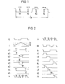
- the drawing Figure 1 shows schematically an embodiment of a pulse frame T, a time division multiplex system according to the invention.
- this pulse frame T R comprises four time slots forming a time channel K1, K2, K3, K4 together with the corresponding time slots preceding and following time slots, in each of which a phase-modulated pulse-shaped signal may be transmissible.
- the signals of one half K1, K2 of the time channels K1 ... K4 are transmitted as pulses in one half of each pulse frame T R , and each in the other half Pulse frame T R , the signals of the other half K3, K4 of the time channels K1 ... K4 are transmitted as pulse pauses.
- the pulse pauses form, so to speak, the difference between a continuous signal in the second half of each pulse frame T R , the amplitude of which corresponds to the pulse amplitude, as indicated in line g in FIG. 2, and subtracted pulses ' and thus the pulse pauses on which they are based as will be explained in more detail below.
- the frame clock frequency component as can also be seen in FIG. 2g, is contained very clearly in the signal mixture transmitted in this way, so that recovery of the frame clock is correspondingly facilitated without, for example, a separate time channel special frame identification signal would have to be transmitted.
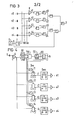
- pulse phase-modulated pulses to be transmitted in one half of the pulse frame and corresponding pulse phase-modulated pulse pauses to be transmitted in the other half of the pulse frame can be done with a circuit arrangement as shown in FIG.
- a sawtooth signal is derived from the pulse frame clock generated by a clock generator G at its output g, as shown in FIG. 2g, via an integrator circuit J, as shown in FIG is indicated;
- This sawtooth signal passes via the integrator output line i to one of the inputs of channel-specific comparators K, which can be implemented by AMD voltage comparators Am685 and whose other inputs are connected to an offset voltage Uu or Uo, as also shown in FIG is indicated.
- the comparators K are acted upon by the respective modulating signals from channel-specific inputs e1, e2, e3, e4.
- the comparator in question is then activated for as long as the sum of the modulating signal and offset voltage exceeds the instantaneous value of the sawtooth signal;
- the resulting pulse-length-modulated signals on the comparator output lines k1, k2, k3, k4 (for example for the instantaneous value zero of the respective modulating signal) are shown in lines 2 in lines k1, k2, k3, k4. From these signals one obtains pulse-phase-modulated pulses occurring on their output lines d1, d2, d3, d4, as shown in FIG. 3, for example, by a delay element and a blocking element, as shown in FIG. 2 in lines d1, d2, d3, d4 are shown.
- the Signal line s can, without being shown in FIG. 3, lead to an electro-optical transmission stage with a laser diode, from which the signal mixture of pulse-phase-modulated pulses and pulse pauses, for example via a broadband switching center with a subscriber line in a broadband communication network connecting optical fiber is optically transmitted.
- the latter In order to recover the frame clock from the transmitted signal mixture at the receiving end, the latter, as can be seen from FIG. 4, can be capacitively coupled from an opto-electrical receiving stage, which is no longer shown in FIG. 4, via a line s then leading the signal mixture according to FIG. 2s Amplitude decider A arrive, which can also be given by an AMD voltage comparator Am 685.
- This amplitude decider regenerates the received pulses and pulse pauses, without a special measurement of the pulse amplitudes and a corresponding adjustment of the decision threshold.
- the frame clock component is filtered out from the regenerated signal mixture as well as the complementary signal by means of a band filter BF, and both signals are fed to a phase comparator Vgl implemented, for example, with the aid of a Siemens mixer S 042, which also has a clock generator circuit GG controlled by a phase comparator controlled by the phase comparator , 2/1 generated frame clock is applied so that it is synchronized with the frame clock contained in the transmitted signal mixture.
- the clock generator circuit comprises a clock generator GG, which generates a clock on its output line gg with a clock frequency equal to twice the frame clock frequency, as shown in line 2 in FIG. 2; this clock generator is GG
- a binary divider 2/1 which carries the frame clock as shown in FIG. 2h, is connected downstream on its output line h and leads to the input side of the comparator Vgl on the output side, possibly via a low-pass switch not shown in FIG.
- logic elements are e.g. acted on in the form of an AND gate or a blocking gate, so that at their outputs f1, f2, f3, f4 corresponding time window signals appear as in FIG. 2 in lines f1, f2, f3, f4 are shown.
- These time window signals are supplied with unlocking inputs from PPM / PLM pulse converters implemented, for example, with the aid of Motorola master-slave D flip-flops MC 1670, which are connected on the input side with the transmitted and.
- the logic circuits generating the time window signals and the PPM / PLM pulse converters unlocked by them in a timely manner are summarized with Dex.
- the pulses or pulse pauses in the form shown in FIG. 2 lines 11, 12, 13, 14 expediently reach a low-pass filter Dem having an attenuation pole at the clock frequency, in which the original modulation signals are recovered and which may then lead to channel-specific outputs a1, a2, a3, a4 via a subsequent video amplifier.
Landscapes
- Engineering & Computer Science (AREA)
- Computer Networks & Wireless Communication (AREA)
- Signal Processing (AREA)
- Time-Division Multiplex Systems (AREA)
- Optical Communication System (AREA)
- Synchronisation In Digital Transmission Systems (AREA)
- Use Of Switch Circuits For Exchanges And Methods Of Control Of Multiplex Exchanges (AREA)
Priority Applications (1)
| Application Number | Priority Date | Filing Date | Title |
|---|---|---|---|
| AT80107322T ATE5789T1 (de) | 1979-11-27 | 1980-11-24 | Zeitmultiplexsystem. |
Applications Claiming Priority (2)
| Application Number | Priority Date | Filing Date | Title |
|---|---|---|---|
| DE19792947770 DE2947770A1 (de) | 1979-11-27 | 1979-11-27 | Zeitmultiplexsystem |
| DE2947770 | 1979-11-27 |
Publications (2)
| Publication Number | Publication Date |
|---|---|
| EP0029607A1 true EP0029607A1 (fr) | 1981-06-03 |
| EP0029607B1 EP0029607B1 (fr) | 1984-01-04 |
Family
ID=6086996
Family Applications (1)
| Application Number | Title | Priority Date | Filing Date |
|---|---|---|---|
| EP80107322A Expired EP0029607B1 (fr) | 1979-11-27 | 1980-11-24 | Système multiplex à division de temps |
Country Status (5)
| Country | Link |
|---|---|
| US (1) | US4414663A (fr) |
| EP (1) | EP0029607B1 (fr) |
| JP (1) | JPS5912058B2 (fr) |
| AT (1) | ATE5789T1 (fr) |
| DE (2) | DE2947770A1 (fr) |
Cited By (2)
| Publication number | Priority date | Publication date | Assignee | Title |
|---|---|---|---|---|
| FR2684824A1 (fr) * | 1991-12-06 | 1993-06-11 | Alcatel Business Systems | Procede de transmission d'informations numeriques entre deux unites d'emission-reception et dispositif mettant en óoeuvre ce procede. |
| FR2694854A1 (fr) * | 1992-08-12 | 1994-02-18 | Trt Telecom Radio Electr | Dispositif pour réaliser un multiplexage-démultiplexage temporel de voies de signaux numériques. |
Families Citing this family (12)
| Publication number | Priority date | Publication date | Assignee | Title |
|---|---|---|---|---|
| DE3211242C2 (de) * | 1982-03-26 | 1985-07-04 | Siemens AG, 1000 Berlin und 8000 München | Verfahren für eine optische Zeitmultiplex-Übertragung über einen Lichtleiter eines Vermittlungssystems insbesondere Fernsprech-Vermittlungssystems |
| US5163072A (en) * | 1986-07-23 | 1992-11-10 | Optical Communications Corporation | Optical communications transmitter and receiver |
| US4952070A (en) * | 1988-10-17 | 1990-08-28 | Rockwell International Corporation | Digital data coding technique |
| US5086435A (en) * | 1988-10-17 | 1992-02-04 | Rockwell International Corporation | Method and apparatus for detecting signals on digital data systems |
| DE4137882A1 (de) * | 1991-02-06 | 1992-10-08 | Andreas Mueller | Vorrichtung zur drahtlosen zweikanal-informationsuebertragung |
| DE4128671A1 (de) * | 1991-08-29 | 1993-04-01 | Sennheiser Electronic | Verfahren zur uebermittlung von analogen nachrichtensignalen ueber einen lichttraeger |
| JPH0795156A (ja) * | 1993-09-20 | 1995-04-07 | Fujitsu Ltd | 光入力断検出回路 |
| DE19654979B4 (de) * | 1995-05-18 | 2006-03-02 | Fujitsu Ltd., Kawasaki | Treiberschaltung für einen optischen Elektroabsorptionsmodulator |
| DE19715636A1 (de) * | 1997-04-15 | 1998-10-22 | Renfer Robert O | Vorrichtung zur drahtlosen optischen Übertragung |
| DE69827885T2 (de) * | 1997-09-02 | 2005-12-01 | Alcatel | Verfahren zur Erzeugung eines Multimodulationsrahmens und zugehöriger Modulator |
| DE10251504A1 (de) * | 2002-11-04 | 2004-05-19 | Endress + Hauser Flowtec Ag, Reinach | Verfahren und Vorrichtung zur Übertragung von digitalen Signalen über einen Optokoppler |
| DE102004049016B3 (de) * | 2004-10-05 | 2005-08-11 | Brinkhus, Hartmut B., Dr. | Schaltungsanordung zur galvanisch getrennten Übertragung eines elektrischen Signals mit einem Optokoppler |
Citations (2)
| Publication number | Priority date | Publication date | Assignee | Title |
|---|---|---|---|---|
| FR1051760A (fr) * | 1954-01-19 | |||
| US3766315A (en) * | 1970-09-11 | 1973-10-16 | Nasa | Method and apparatus for a single channel digital communications system |
Family Cites Families (3)
| Publication number | Priority date | Publication date | Assignee | Title |
|---|---|---|---|---|
| US3402264A (en) * | 1964-05-22 | 1968-09-17 | Honeywell Inc | Digital synchronizer |
| US3898388A (en) * | 1974-06-21 | 1975-08-05 | United Aircraft Corp | Phase inversion synchronization |
| US4054754A (en) * | 1976-06-07 | 1977-10-18 | Bell Telephone Laboratories, Incorporated | Arrangement for transmitting digital data and synchronizing information |
-
1979
- 1979-11-27 DE DE19792947770 patent/DE2947770A1/de not_active Withdrawn
-
1980
- 1980-11-05 US US06/204,207 patent/US4414663A/en not_active Expired - Lifetime
- 1980-11-24 DE DE8080107322T patent/DE3066064D1/de not_active Expired
- 1980-11-24 EP EP80107322A patent/EP0029607B1/fr not_active Expired
- 1980-11-24 AT AT80107322T patent/ATE5789T1/de not_active IP Right Cessation
- 1980-11-27 JP JP55165987A patent/JPS5912058B2/ja not_active Expired
Patent Citations (2)
| Publication number | Priority date | Publication date | Assignee | Title |
|---|---|---|---|---|
| FR1051760A (fr) * | 1954-01-19 | |||
| US3766315A (en) * | 1970-09-11 | 1973-10-16 | Nasa | Method and apparatus for a single channel digital communications system |
Non-Patent Citations (1)
| Title |
|---|
| TELECOMMUNICATIONS AND RADIO ENGINEERING, Band 27/28, Nr. 10, Oktober 1974, Washington, US, V.B. BRAUDE: "Some methods of obtaining a synchronization signal in optical pulse code modulation-time division communications channels", Seiten 64-68 * Seite 64, Zeilen 19-30; Seite 65, Zeilen 27,28; Figur 1a * * |
Cited By (2)
| Publication number | Priority date | Publication date | Assignee | Title |
|---|---|---|---|---|
| FR2684824A1 (fr) * | 1991-12-06 | 1993-06-11 | Alcatel Business Systems | Procede de transmission d'informations numeriques entre deux unites d'emission-reception et dispositif mettant en óoeuvre ce procede. |
| FR2694854A1 (fr) * | 1992-08-12 | 1994-02-18 | Trt Telecom Radio Electr | Dispositif pour réaliser un multiplexage-démultiplexage temporel de voies de signaux numériques. |
Also Published As
| Publication number | Publication date |
|---|---|
| JPS5687955A (en) | 1981-07-17 |
| ATE5789T1 (de) | 1984-01-15 |
| US4414663A (en) | 1983-11-08 |
| DE3066064D1 (en) | 1984-02-09 |
| DE2947770A1 (de) | 1981-07-23 |
| EP0029607B1 (fr) | 1984-01-04 |
| JPS5912058B2 (ja) | 1984-03-21 |
Similar Documents
| Publication | Publication Date | Title |
|---|---|---|
| EP0029607A1 (fr) | Système multiplex à division de temps | |
| EP0304799B1 (fr) | Dispositif pour démoduler un signal biphasé | |
| DE3442613C2 (fr) | ||
| DE1537638B2 (de) | Übertragungssystem mit einer Sende- und einer Empfangsvorrichtung zur Übertragung von Informationen in einem vorgeschriebenen Frequenzband sowie dabei zu verwendende Sende- und Empfangsvorrichtungen | |
| DE3344074A1 (de) | Verfahren und anordnung zur fernueberwachung einer digitaluebertragungsstrecke | |
| DE3224425A1 (de) | Bussystem mit lichtwellenleitern | |
| DE3125724C2 (fr) | ||
| DE69323694T2 (de) | Übertragungsnetz mit Vielfachzugriff | |
| EP0053230A1 (fr) | Système numérique de transmission d'information | |
| DE1928986A1 (de) | UEbertragungssystem mit einer Sende- und einer Empfangsvorrichtung zur UEbertragung von Informationen in einem vorgeschriebenen Frequenzband und dafuer geeignete Sende- und Empfangsvorrichtungen | |
| DE2850129A1 (de) | Schaltungsanordnung zur umwandlung von binaeren digitalsignalen in pseudoternaere wechselimpulse | |
| EP0817407A2 (fr) | Dispositif et unité d'émission et système de transmission optique pour transmettre des signaux électriques analogiques | |
| DE3526051A1 (de) | Digitales nachrichtenuebertragungssystem mit einem nb/(n+1)b-leitungscode | |
| EP0995286A1 (fr) | Procedure de transmission d'informations de signalisation et de commande pour reseaux a multiplexage en longueur d'onde destines a la transmission d'informations optique par fibres | |
| DE3526052A1 (de) | Digitales nachrichtenuebertragungssystem mit einem nb/(n+1)b-leitungscode | |
| EP0140043A2 (fr) | Décodeur pour code HDB3 à deux niveaux | |
| DE2817646A1 (de) | Verfahren und einrichtung zur streckenmessung in elektrischen nachrichtenuebertragungssystemen | |
| DE2159187C3 (de) | Verfahren zur wahlweisen Demodulation eines oder mehrerer, insbesondere zweier, durch Mehrfachfrequenzumtastung kombinierter Fernschreibkanäle und Schaltungsanordnung zur Durchführung des Verfahrens | |
| DE3230271C2 (fr) | ||
| DE2748154A1 (de) | Datenuebertragungssystem mit pulslagemodulation | |
| DE2115927C (de) | Verfahren zur Übertragung zusätzlicher Informationen bei der Übertragung von Daten | |
| DE3229417C2 (fr) | ||
| DE2051266A1 (de) | Nachrichtenübertragungssystem mit Pulscodemodulation | |
| DE1087166B (de) | Sendeeinrichtung fuer Zweiercodefrequenzmodulation | |
| EP0271955A2 (fr) | Circuit pour la synchronisation de dispositifs dans des centraux et des stations d'amplification d'un système de transmission par répartition dans le temps |
Legal Events
| Date | Code | Title | Description |
|---|---|---|---|
| PUAI | Public reference made under article 153(3) epc to a published international application that has entered the european phase |
Free format text: ORIGINAL CODE: 0009012 |
|
| AK | Designated contracting states |
Designated state(s): AT BE CH DE FR GB IT NL SE |
|
| 17P | Request for examination filed |
Effective date: 19811028 |
|
| ITF | It: translation for a ep patent filed | ||
| GRAA | (expected) grant |
Free format text: ORIGINAL CODE: 0009210 |
|
| AK | Designated contracting states |
Designated state(s): AT BE CH DE FR GB IT LI NL SE |
|
| PG25 | Lapsed in a contracting state [announced via postgrant information from national office to epo] |
Ref country code: SE Effective date: 19840104 Ref country code: NL Effective date: 19840104 |
|
| REF | Corresponds to: |
Ref document number: 5789 Country of ref document: AT Date of ref document: 19840115 Kind code of ref document: T |
|
| REF | Corresponds to: |
Ref document number: 3066064 Country of ref document: DE Date of ref document: 19840209 |
|
| ET | Fr: translation filed | ||
| NLV1 | Nl: lapsed or annulled due to failure to fulfill the requirements of art. 29p and 29m of the patents act | ||
| PLBE | No opposition filed within time limit |
Free format text: ORIGINAL CODE: 0009261 |
|
| STAA | Information on the status of an ep patent application or granted ep patent |
Free format text: STATUS: NO OPPOSITION FILED WITHIN TIME LIMIT |
|
| PGFP | Annual fee paid to national office [announced via postgrant information from national office to epo] |
Ref country code: FR Payment date: 19841120 Year of fee payment: 5 |
|
| PG25 | Lapsed in a contracting state [announced via postgrant information from national office to epo] |
Ref country code: AT Effective date: 19841124 |
|
| PG25 | Lapsed in a contracting state [announced via postgrant information from national office to epo] |
Ref country code: LI Effective date: 19841130 Ref country code: CH Effective date: 19841130 |
|
| PGFP | Annual fee paid to national office [announced via postgrant information from national office to epo] |
Ref country code: BE Payment date: 19841231 Year of fee payment: 5 |
|
| 26N | No opposition filed | ||
| PGFP | Annual fee paid to national office [announced via postgrant information from national office to epo] |
Ref country code: DE Payment date: 19850129 Year of fee payment: 5 |
|
| REG | Reference to a national code |
Ref country code: CH Ref legal event code: PL |
|
| PG25 | Lapsed in a contracting state [announced via postgrant information from national office to epo] |
Ref country code: BE Effective date: 19871130 |
|
| BERE | Be: lapsed |
Owner name: SIEMENS A.G. BERLIN UND MUNCHEN Effective date: 19871130 |
|
| GBPC | Gb: european patent ceased through non-payment of renewal fee | ||
| PG25 | Lapsed in a contracting state [announced via postgrant information from national office to epo] |
Ref country code: FR Free format text: LAPSE BECAUSE OF NON-PAYMENT OF DUE FEES Effective date: 19880729 |
|
| PG25 | Lapsed in a contracting state [announced via postgrant information from national office to epo] |
Ref country code: DE Effective date: 19880802 |
|
| REG | Reference to a national code |
Ref country code: FR Ref legal event code: ST |
|
| PG25 | Lapsed in a contracting state [announced via postgrant information from national office to epo] |
Ref country code: GB Effective date: 19881118 |