EP0029987A2 - Dispositif semiconducteur - Google Patents
Dispositif semiconducteur Download PDFInfo
- Publication number
- EP0029987A2 EP0029987A2 EP80107316A EP80107316A EP0029987A2 EP 0029987 A2 EP0029987 A2 EP 0029987A2 EP 80107316 A EP80107316 A EP 80107316A EP 80107316 A EP80107316 A EP 80107316A EP 0029987 A2 EP0029987 A2 EP 0029987A2
- Authority
- EP
- European Patent Office
- Prior art keywords
- region
- conductivity type
- main surface
- collar
- base region
- Prior art date
- Legal status (The legal status is an assumption and is not a legal conclusion. Google has not performed a legal analysis and makes no representation as to the accuracy of the status listed.)
- Granted
Links
Images



Classifications
-
- H—ELECTRICITY
- H10—SEMICONDUCTOR DEVICES; ELECTRIC SOLID-STATE DEVICES NOT OTHERWISE PROVIDED FOR
- H10D—INORGANIC ELECTRIC SEMICONDUCTOR DEVICES
- H10D84/00—Integrated devices formed in or on semiconductor substrates that comprise only semiconducting layers, e.g. on Si wafers or on GaAs-on-Si wafers
- H10D84/01—Manufacture or treatment
- H10D84/0112—Integrating together multiple components covered by H10D8/00, H10D10/00 or H10D18/00, e.g. integrating multiple BJTs
- H10D84/0116—Integrating together multiple components covered by H10D8/00, H10D10/00 or H10D18/00, e.g. integrating multiple BJTs the components including integrated injection logic [I2L]
-
- H—ELECTRICITY
- H10—SEMICONDUCTOR DEVICES; ELECTRIC SOLID-STATE DEVICES NOT OTHERWISE PROVIDED FOR
- H10D—INORGANIC ELECTRIC SEMICONDUCTOR DEVICES
- H10D10/00—Bipolar junction transistors [BJT]
- H10D10/40—Vertical BJTs
- H10D10/461—Inverted vertical BJTs
-
- H—ELECTRICITY
- H10—SEMICONDUCTOR DEVICES; ELECTRIC SOLID-STATE DEVICES NOT OTHERWISE PROVIDED FOR
- H10D—INORGANIC ELECTRIC SEMICONDUCTOR DEVICES
- H10D62/00—Semiconductor bodies, or regions thereof, of devices having potential barriers
- H10D62/10—Shapes, relative sizes or dispositions of the regions of the semiconductor bodies; Shapes of the semiconductor bodies
- H10D62/13—Semiconductor regions connected to electrodes carrying current to be rectified, amplified or switched, e.g. source or drain regions
- H10D62/133—Emitter regions of BJTs
-
- H—ELECTRICITY
- H10—SEMICONDUCTOR DEVICES; ELECTRIC SOLID-STATE DEVICES NOT OTHERWISE PROVIDED FOR
- H10D—INORGANIC ELECTRIC SEMICONDUCTOR DEVICES
- H10D84/00—Integrated devices formed in or on semiconductor substrates that comprise only semiconducting layers, e.g. on Si wafers or on GaAs-on-Si wafers
- H10D84/01—Manufacture or treatment
- H10D84/02—Manufacture or treatment characterised by using material-based technologies
- H10D84/03—Manufacture or treatment characterised by using material-based technologies using Group IV technology, e.g. silicon technology or silicon-carbide [SiC] technology
- H10D84/038—Manufacture or treatment characterised by using material-based technologies using Group IV technology, e.g. silicon technology or silicon-carbide [SiC] technology using silicon technology, e.g. SiGe
-
- H—ELECTRICITY
- H10—SEMICONDUCTOR DEVICES; ELECTRIC SOLID-STATE DEVICES NOT OTHERWISE PROVIDED FOR
- H10D—INORGANIC ELECTRIC SEMICONDUCTOR DEVICES
- H10D84/00—Integrated devices formed in or on semiconductor substrates that comprise only semiconducting layers, e.g. on Si wafers or on GaAs-on-Si wafers
- H10D84/60—Integrated devices formed in or on semiconductor substrates that comprise only semiconducting layers, e.g. on Si wafers or on GaAs-on-Si wafers characterised by the integration of at least one component covered by groups H10D10/00 or H10D18/00, e.g. integration of BJTs
- H10D84/65—Integrated injection logic
- H10D84/658—Integrated injection logic integrated in combination with analog structures
-
- H—ELECTRICITY
- H10—SEMICONDUCTOR DEVICES; ELECTRIC SOLID-STATE DEVICES NOT OTHERWISE PROVIDED FOR
- H10W—GENERIC PACKAGES, INTERCONNECTIONS, CONNECTORS OR OTHER CONSTRUCTIONAL DETAILS OF DEVICES COVERED BY CLASS H10
- H10W20/00—Interconnections in chips, wafers or substrates
- H10W20/01—Manufacture or treatment
- H10W20/021—Manufacture or treatment of interconnections within wafers or substrates
Definitions
- the present invention relates to a semiconductor device and its manufacturing method and, more particularly, to a semiconductor device having a bipolar transistor with an improved current amplification factor as reversely operates with respect to the conventional transistor and its manufacturing method.
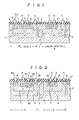
- I 2 L circuit An integrated injection logic (I 2 L) circuit is known as an integrated circuit including a bipolar transistor as reversely operates. Part of the integrated circuit of this type is illustrated in cross section in Fig. 1 and is disclosed in IEEE, J, of Solid-State circuits, SC-9, PP, 206 to 283, 1971.
- I 2 L gate 3 and a linear npn transistor 4 are formed on a p-type semiconductor substrate 1, with a p + isolation region 2 disposed therebetween. Only the I 2 L gate will be described for simplicity.
- On the p-type substrate 1 are formed an n + -type buried region 5, an n +- type collar region 6 and an n-type region 7.
- n-type injector region 8 Within the n-type region 7 are formed a p-type injector region 8, a p-type base region 9, and an n + -type collector region 10 formed within the p-type base region 9.
- INJ, B, C and E represent injector, base, collector and emitter terminals, respectively.
- Those semiconductor regions 7, 9 and 10 cooperate to form a bipolar transistor as operates reversely.
- bipolar transistor as operates reversely means a transistor of the type in which the base current flows into the collector and will often be referred to as a upside-down transistor.
- the n collar region 6 prevents holes injected from the base region 9 from flowing laterally, thereby to increase a current amplification factor of an npn transistor of the reverse-operation type.
- the impurity concentration of the n + collar region 6 is higher. Further, it is necessary that the region 6 is diposed closest to the base region 9.
- the collar region 6 was formed in a manner that phosphorus is diffused at high concentration from the main surface of the semiproduct by using phosphorus oxychloride (POC2 3 ).
- POC2 3 phosphorus oxychloride
- the current amplification factor of the upside-down npn transistor descreases contrary to expectation. Therefore, the surface concentration of the n collar region 6 can not be increased sufficiently and the current amplification factor of the upside-down npn transistor can not be increased.
- an object of the present invention is to provide a semiconductor device including the upside-down bipolar transistor of which the reverse-directional current amplification factor is remarkably increased by completely removing the lattice defects in the n + collar region, and a manufacturing method of the semiconductor device.
- a semiconductor device comprises a semiconductor region of a second conductivity type; a bipolar transistor as reversely operates which is formed in the semiconductor region of the second conductivity type at main surface side thereof, and has a first conductivity base region; and a collar region of the second conductivity type which is deeper than the base region, contacts with or is close to the base region, and extends opposite to the main surface of the second conductivity type region; the collar region being formed by diffusing phosphorus and arsenic at high concentration.
- a method of fabricating a semiconductor device comprising steps of forming a bipolar transistor as operates reversely having a first conductivity type base region in a semiconductor region of a second conductivity type of which the main surface has the crystalline direction of ⁇ 111 > , and forming a collar region, which is in contact with or is close to the base region and extends opposite to the main surface of the second conductivity type semiconductor region, by diffusing phosphorus and arsenic.
- Fig.2 illustrating in cross section an embodiment of the semiconductor device including the I 2 L gate 3 and the npn linear transistor 4, which are formed on the p-type substrate 1, like Fig. 1.
- the I 2 L gate 3 includes the n + region 5, the injector region 8 formed in the n-type region 7 enclosed by the n region 5 and n collar region 18, an external base region 9a, an internal base region 9b, and the n collector region 10 enclosed by the external base region 9a and the internal base region 9b.
- Those regions 5, 18, 7, 9a, 9b and 10 cooperate to form the upside-down bipolar transistor.
- the npn linear tan- sistor 4 is electrically separated from I 2 L gate 3 by the p isolation region 2, and is comprised of the n + region 5, an n + high concentration collector region 21, the n-type region 7, a p-type base region 19, and an emitter region 20 enclosed by the base region 19.
- the regions, 8, 9a, 10 and 18 are connected to its related circuit by electrodes INT, B, C and E.
- the regions 20, 19 and 21 are connected to its related circuit by the electrodes E, B and C.
- the n + collar region 18 of the I 2 L gate extends to the n region 5 in contact with or close to the base region 9a.
- the feature of the present invention resides in that the collar region 18 is formed by diffusing phosphous and arsenic at high concentration.
- the n + high concentration collector region 21 of the npn linear transistor 4 is also formed in the same manner.
- Reference numeral 17 designates an insulating layer.
- Figs. 3A to 3F An example of the manufacturing method of the semiconductor deivce shown in Fig. 2 will be described referring to Figs. 3A to 3F.
- the fan-out of the 1 2 L gate 3 of the device shown in Fig. 2 is one, two or more fan outs, npn linear transistors, resistors and capacitors and the like may be formed on the same chip.
- impurity material such as Sb, As and P is diffused from the main surface of the P type substrate 1 having a specific resistance of 10 ⁇ cm, of which the crystalline direction is ⁇ 111 > thereby to from the n buried region 5 and then the n-type epitaxial region 7.
- the breakdown voltage between the emitter and the collector of the linear transistor 4 is demanded to be 10 V or more, it is preferable to use the semiconductor substrate 1 with the (111) surface as the inversion voltage of a field region can be raised.
- the specific resistance and the thickness of the n-type epitaxial region 7 are determined by considering the breakdown voltage necessary for the linear transistor 4 coexisting with the I 2 L gate. Normally, those are selected to be 0.5 ⁇ cm to 2 ⁇ cm for the specific resistance and 5 ⁇ m to 20 ⁇ m for the thickness. Then, as shown in Fig.
- a thermal oxidation layer 22 (SiO 2 layer) is formed on the surface of the epitaxial region 7, holes 23 are formed at the locations corresponding to regions to be p isolation regions 2, an insulating layer 24 containing boron is formed on the oxidation layer 22, and the p isolation regions 2 are formed by diffusing boron.
- Boron silicate glass (BSG) containing boron at high concentration is generally used for the insulating layer 24.
- the thermal oxidation layer (SiO 2 layer) 25 is again formed with the thickness from about 1000 ⁇ to 3000 ⁇ , as shown in Fig. 3C. Further, a resist pattern 26 is formed on the layer 25.
- An intrinsic base region 11 is formed by injecting boron ions into an instrinsic base region (the region for forming the internal base region 9b shown in Fig. 2) of the I 2 L gate 3, by using the resist pattern as a mask. At this time, if necessary, boron is also injected into another region to form a high resistor, at the dosage of 5 x 10 12 cm-2 13 -2 to 3 x 10 cm .
- the acceleration voltage of the injecting ions depends on the thickness of the thermal oxidation layer 25, usually 50 keV to 200 keV.
- the depth of the intrinsic base region 11 is selected to be aprroximately 2.5 to 4 ⁇ m. Then, the resist pattern 26 is removed and a silicon dioxide layer 27 is formed, as shown in Fig.
- the (P + As) layer may be formed by mixing a mixed gas containing P H3 and AsH 3 at the flow rate ratio of 4 : 1, into the gas containing SiH 4 and 0 2 when they are thermally decomposed.
- the n + collar region 18 and the high concentration collector region 21 may be formed by diffusing P and As at about 1100°C by using the (P + As) layer as a diffusion source.
- the depth of the n + collar region 18 must be deeper than the depth of the intrinsic base region 11.
- the diffusion coefficient phophorus is larger than that of arsenic. Therefore, the n collar region 18 contains the phosphorus diffused deeply from the surface thereof and arsenic diffused shallowly from the surface. In this way, by simultane- nously diffusing phosphorus and arsenic, the lattice defects (dislocation and the like) may be minimized which occurs in the collar region 18.
- Indivisual diffusion of phosphorus and arsenic may also effect the restriction of the lattice defect occurence.
- a preferable ratio of arsenic to phosphorus ranges 3 % to 40 % in the number of atoms.
- the number 3 of the lattice deffects was 10 cm .
- Such number of lattice defects of 10 3 cm -2 were negligible in practical use.
- the number of the lattice defects (dislocation densitty) in 5 the surface of the collar region 18 was 10 cm .
- the present invention may improve the lattice defects density of the n + collar region 18 by two or more orders when compared to the conventional method.
- the saturation voltage U CE (SAT) of the n p n transistor 4 may be decreased.
- the dislocation is most likely to occur in the crystalline direction of ⁇ 110 > in the equivalent surfaces of (111).
- the dislocation When only phosphorus is duffused into a region to be the n + collar region 18 and a region to be the high concentration collector region 21 by the conventional process, a number of the dislocations take place in those regions. In this case, the dislocation extends into the equivalent surfaces of (111) in the peripheral semiconductor region. The rate of the extension of the dislocation is specially accelerated near the surface of the semiconductor region.
- the low saturation voltage is not required for the linear npn transistor 4 in its operation, there is no need of the high concentration for the collector region 21.
- a pnp transistor (not shown) is provided on the chip on which the I 2 L gate 3 is formed, it is very effective to diffuse at high concentration phosphorus and arsenic in the base region of the pnp transistor. Specailly in the pnp transistor with a large current, the reduction of the base resistance is remarkably important and it is possible to prevent reduction of the current amplification factor in a large current range.
- the (P + As) layer 29, the CVD silicon dioxide layer 27, and the thermal oxidation layer 25 are removed.
- a thermal silicon dioxide layer 30 is formed, as shown in Fig. 3E and a resist pattern 31 is further formed as an ion injection mask on the layer 30.
- boron ion is injected into the external base region 9a of the I 2 L gate 3, the injector region 8, and the base region 19 of the npn transistor 4.
- the concentration of the boron in the base region 19 is selected higher than that of the boron in the intrinsic base region 11, for the purpose of decreasing the specific resistance of the base region 19.
- the dosage of boron to be injected is selected to be 1 x 10 14 cm-2and the acceleration voltage is selected to be 50 keV to 300 keV.
- the depth of the base region 19 is approxiamtely 2 ⁇ m to 3.5 N m, slightly shallower than the intrinsic base region 11.
- the resist pattern 31 is removed and a CV D silicon dioxide layer 32 is deposited on the thermal silicon dioxide layer 30, as shown in Fig. 3F.
- holes are provided through the thermal silicon dioxide layer 30 and the CVD silicon dioxide layer 32 at the portions corresponding to the collector region 12 of the I 2 L gate 3 and the emitter region 20 of the npn transistor 4, as shown in Fig. 3F.
- the insulating layer 30, 32 and 33 are holed at the portions corresponding to the regions 8, 9a, 12 and 18 of the I 2 L gate 3 and the regions 20, 19 and 21 of the npn transistor 4 and electrodes for interconnections denoted as IN, B, C and E are formed.
- the fabrication process of the semiconductor device is completed.
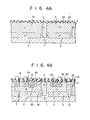
- Figs. 4A and 4B illustrate a manufacturing process of another embodiment of the present invention.
- an epitaxial layer n -1 7 with a specific resistance of 2 ⁇ cm to 10 ⁇ cm is formed on a p-type substrate 1.
- phosphorus is deeply diffused into only one epitaxial layer of the epitaxial layers on which the I 2 L layer is formed thereby to form an n well region 7a.
- the specific resistance of the n well region 7a may be reduced to approximately 0.1 ⁇ cm.
- the switching speed of the I 2 L gate is increased to be about two times that when no n well region 7a is provided.
- the steps shown in Figs. 3C to 3D are performed to form the semiconductor device shown in Fig. 4B.
- the reverse gain up of the reverse operation transistor was 30; an input frequency of a T-type flip-flop formed by the I L gate was 3 MHz; the power delay time product of the I 2 L gate was 0.18 pJ (pico joule), the emitter-collector breakdown voltage (VCEO) was 40 V or more. Those values can not be obtained by the conventional device.
- Fig. 5A is a microscopic photograph for illustrating lattice detects when the collar region 18 is formed by using phosphorus oxychloride POCl 3 .
- Fig. 5B is a microscopic photograph for illustrating the lattice defects when the collar region 18 is formed by diffusing phosphorus and arsenic according to this invention in place of POCl 3 .
- the semiconductor devices of the both are fabricated by the same process except for the diffusion process of the collar region 18.
- the chips of the I 2 L gates of the both were etched by the Wright etching solution.
- triangular etch pits arising from the disclocation occuring in the collar region overflows into the active region other than the n + collar region.
- the lattice defects occuring in the n + collar region may be restrained when the n + collar region is formed by diffusing phosphorus and arsenic.
- the lattice defects of the n + collar region extends up to the active element region other than the I 2 L gate. Therefore, in order to increase the current amplification factor of the reverse operation transistor, it is essential to prevent the lattice defects from occuring in the n + collar region.
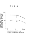
- a curve 35 represents the ⁇ up - Ic relation of the upside-down transistor fabricated by the present invention.
- a curve 36 represents that of the transistor formed by the conventional process.
- the maximum value of the ⁇ up is 45, which is about three times of the maximum ⁇ up in the curve 36.
- the ⁇ up is decreased in the curve 36 while it is not decreased in the curve 35. It is apparent that the increase of the ⁇ up improves the operation speed of the 1 2 L gate and the noise margin is increased.
- the present invention which has been described by using the embodiment having the reverse operation npn transistor coexisting with the injector region, may of course be applied for the upside-down npn transistor not coexisting therewith.
- the lattice defects in the high concentration collector region enters the base region, so that phosphorus is abnormaly diffused into the emitter region of the linear transistor. Because of this, the breakdown voltage between the emitter and collector of the linear npn transistor was reduced.
- the present invention solves this problem by forming the high concentration region of the linear npn transistor by diffusing phosphorus and arsenic. As a result, the yield of products is improved about two times compared to the conventional technique.
Landscapes
- Bipolar Transistors (AREA)
- Bipolar Integrated Circuits (AREA)
Applications Claiming Priority (2)
| Application Number | Priority Date | Filing Date | Title |
|---|---|---|---|
| JP15360479A JPS5676564A (en) | 1979-11-29 | 1979-11-29 | Semiconductor device and manufacture thereof |
| JP153604/79 | 1979-11-29 |
Publications (3)
| Publication Number | Publication Date |
|---|---|
| EP0029987A2 true EP0029987A2 (fr) | 1981-06-10 |
| EP0029987A3 EP0029987A3 (en) | 1983-01-19 |
| EP0029987B1 EP0029987B1 (fr) | 1986-04-16 |
Family
ID=15566109
Family Applications (1)
| Application Number | Title | Priority Date | Filing Date |
|---|---|---|---|
| EP80107316A Expired EP0029987B1 (fr) | 1979-11-29 | 1980-11-24 | Dispositif semiconducteur |
Country Status (3)
| Country | Link |
|---|---|
| EP (1) | EP0029987B1 (fr) |
| JP (1) | JPS5676564A (fr) |
| DE (1) | DE3071559D1 (fr) |
Cited By (1)
| Publication number | Priority date | Publication date | Assignee | Title |
|---|---|---|---|---|
| EP0250869A1 (fr) * | 1986-05-27 | 1988-01-07 | Kabushiki Kaisha Toshiba | Circuit intégré semi-conducteur comportant des composants analogiques et numériques |
Families Citing this family (2)
| Publication number | Priority date | Publication date | Assignee | Title |
|---|---|---|---|---|
| JPS5812351A (ja) * | 1981-07-15 | 1983-01-24 | Toshiba Corp | 半導体装置 |
| DE3679947D1 (de) * | 1985-08-26 | 1991-08-01 | Toshiba Kawasaki Kk | Halbleiteranordnungen und verfahren zur herstellung mittels ionenimplantation. |
Family Cites Families (2)
| Publication number | Priority date | Publication date | Assignee | Title |
|---|---|---|---|---|
| US3812519A (en) * | 1970-02-07 | 1974-05-21 | Tokyo Shibaura Electric Co | Silicon double doped with p and as or b and as |
| JPS5325511B2 (fr) * | 1972-08-31 | 1978-07-27 |
-
1979
- 1979-11-29 JP JP15360479A patent/JPS5676564A/ja active Pending
-
1980
- 1980-11-24 DE DE8080107316T patent/DE3071559D1/de not_active Expired
- 1980-11-24 EP EP80107316A patent/EP0029987B1/fr not_active Expired
Cited By (2)
| Publication number | Priority date | Publication date | Assignee | Title |
|---|---|---|---|---|
| EP0250869A1 (fr) * | 1986-05-27 | 1988-01-07 | Kabushiki Kaisha Toshiba | Circuit intégré semi-conducteur comportant des composants analogiques et numériques |
| US4935800A (en) * | 1986-05-27 | 1990-06-19 | Kabushiki Kaisha Toshiba | Semiconductor integrated circuit |
Also Published As
| Publication number | Publication date |
|---|---|
| EP0029987B1 (fr) | 1986-04-16 |
| JPS5676564A (en) | 1981-06-24 |
| DE3071559D1 (en) | 1986-05-22 |
| EP0029987A3 (en) | 1983-01-19 |
Similar Documents
| Publication | Publication Date | Title |
|---|---|---|
| EP0137906B1 (fr) | Procédé de fabrication de transistors NPN verticaux et PNP latéraux dans le même corps semiconducteur | |
| KR900005124B1 (ko) | 상보형 반도체장치 | |
| US3655457A (en) | Method of making or modifying a pn-junction by ion implantation | |
| CA1241770A (fr) | Methode de fabrication de regions auto-alignees en siliciure de metal pour circuits integres a electrodes auto-alignees en silicium polycristallin | |
| US4299024A (en) | Fabrication of complementary bipolar transistors and CMOS devices with poly gates | |
| US3861968A (en) | Method of fabricating integrated circuit device structure with complementary elements utilizing selective thermal oxidation and selective epitaxial deposition | |
| US4066473A (en) | Method of fabricating high-gain transistors | |
| US4111724A (en) | Method of manufacturing oxide isolated semiconductor device utilizing selective etching technique | |
| EP0188291A2 (fr) | Dispositif semi-conducteur bipolaire et son procédé de fabrication | |
| US5554554A (en) | Process for fabricating two loads having different resistance levels in a common layer of polysilicon | |
| US3993513A (en) | Combined method for fabricating oxide-isolated vertical bipolar transistors and complementary oxide-isolated lateral bipolar transistors and the resulting structures | |
| JPS6140146B2 (fr) | ||
| US5089429A (en) | Self-aligned emitter bicmos process | |
| DE3781573T2 (de) | Selbstausrichtender kontakt auf einer diffundierten zone des p-typs. | |
| US4545113A (en) | Process for fabricating a lateral transistor having self-aligned base and base contact | |
| DE69232348T2 (de) | Integrierte Halbleiterschaltungsanordnung und Verfahren zu ihrer Herstellung | |
| EP0139130A1 (fr) | Procédé de fabrication d'un circuit intégré à transistor à haute performance et circuit intégré ainsi réalisé | |
| CA1179786A (fr) | Transistor a structure laterale ayant une base auto-alignee et un contact de base et methode de fabrication | |
| US4783422A (en) | Process for fabricating a bipolar transistor utilizing sidewall masking over the emitter | |
| US5014106A (en) | Semiconductor device for use in a hybrid LSI circuit | |
| US3730787A (en) | Method of fabricating semiconductor integrated circuits using deposited doped oxides as a source of dopant impurities | |
| US5116770A (en) | Method for fabricating bipolar semiconductor devices | |
| US4752817A (en) | High performance integrated circuit having modified extrinsic base | |
| JPS5936432B2 (ja) | 半導体装置の製造方法 | |
| EP0029987B1 (fr) | Dispositif semiconducteur |
Legal Events
| Date | Code | Title | Description |
|---|---|---|---|
| PUAI | Public reference made under article 153(3) epc to a published international application that has entered the european phase |
Free format text: ORIGINAL CODE: 0009012 |
|
| 17P | Request for examination filed |
Effective date: 19801124 |
|
| AK | Designated contracting states |
Designated state(s): DE FR GB NL |
|
| PUAL | Search report despatched |
Free format text: ORIGINAL CODE: 0009013 |
|
| AK | Designated contracting states |
Designated state(s): DE FR GB NL |
|
| RAP1 | Party data changed (applicant data changed or rights of an application transferred) |
Owner name: KABUSHIKI KAISHA TOSHIBA |
|
| GRAA | (expected) grant |
Free format text: ORIGINAL CODE: 0009210 |
|
| AK | Designated contracting states |
Kind code of ref document: B1 Designated state(s): DE FR GB NL |
|
| REF | Corresponds to: |
Ref document number: 3071559 Country of ref document: DE Date of ref document: 19860522 |
|
| ET | Fr: translation filed | ||
| PLBE | No opposition filed within time limit |
Free format text: ORIGINAL CODE: 0009261 |
|
| STAA | Information on the status of an ep patent application or granted ep patent |
Free format text: STATUS: NO OPPOSITION FILED WITHIN TIME LIMIT |
|
| 26N | No opposition filed | ||
| REG | Reference to a national code |
Ref country code: GB Ref legal event code: 746 Effective date: 19980917 |
|
| PGFP | Annual fee paid to national office [announced via postgrant information from national office to epo] |
Ref country code: FR Payment date: 19991109 Year of fee payment: 20 |
|
| PGFP | Annual fee paid to national office [announced via postgrant information from national office to epo] |
Ref country code: GB Payment date: 19991124 Year of fee payment: 20 |
|
| PGFP | Annual fee paid to national office [announced via postgrant information from national office to epo] |
Ref country code: DE Payment date: 19991129 Year of fee payment: 20 |
|
| PGFP | Annual fee paid to national office [announced via postgrant information from national office to epo] |
Ref country code: NL Payment date: 19991130 Year of fee payment: 20 |
|
| REG | Reference to a national code |
Ref country code: FR Ref legal event code: D6 |
|
| PG25 | Lapsed in a contracting state [announced via postgrant information from national office to epo] |
Ref country code: GB Free format text: LAPSE BECAUSE OF EXPIRATION OF PROTECTION Effective date: 20001123 |
|
| PG25 | Lapsed in a contracting state [announced via postgrant information from national office to epo] |
Ref country code: NL Free format text: LAPSE BECAUSE OF EXPIRATION OF PROTECTION Effective date: 20001124 |
|
| REG | Reference to a national code |
Ref country code: GB Ref legal event code: PE20 Effective date: 20001123 |
|
| NLV7 | Nl: ceased due to reaching the maximum lifetime of a patent |
Effective date: 20001124 |