EP0030422A2 - Dispositif de mémoire à semi-conducteurs - Google Patents
Dispositif de mémoire à semi-conducteurs Download PDFInfo
- Publication number
- EP0030422A2 EP0030422A2 EP80304083A EP80304083A EP0030422A2 EP 0030422 A2 EP0030422 A2 EP 0030422A2 EP 80304083 A EP80304083 A EP 80304083A EP 80304083 A EP80304083 A EP 80304083A EP 0030422 A2 EP0030422 A2 EP 0030422A2
- Authority
- EP
- European Patent Office
- Prior art keywords
- memory
- word line
- transistors
- cell
- set forth
- Prior art date
- Legal status (The legal status is an assumption and is not a legal conclusion. Google has not performed a legal analysis and makes no representation as to the accuracy of the status listed.)
- Granted
Links
Images








Classifications
-
- H—ELECTRICITY
- H03—ELECTRONIC CIRCUITRY
- H03K—PULSE TECHNIQUE
- H03K3/00—Circuits for generating electric pulses; Monostable, bistable or multistable circuits
- H03K3/02—Generators characterised by the type of circuit or by the means used for producing pulses
- H03K3/26—Generators characterised by the type of circuit or by the means used for producing pulses by the use, as active elements, of bipolar transistors with internal or external positive feedback
- H03K3/28—Generators characterised by the type of circuit or by the means used for producing pulses by the use, as active elements, of bipolar transistors with internal or external positive feedback using means other than a transformer for feedback
- H03K3/281—Generators characterised by the type of circuit or by the means used for producing pulses by the use, as active elements, of bipolar transistors with internal or external positive feedback using means other than a transformer for feedback using at least two transistors so coupled that the input of one is derived from the output of another, e.g. multivibrator
- H03K3/286—Generators characterised by the type of circuit or by the means used for producing pulses by the use, as active elements, of bipolar transistors with internal or external positive feedback using means other than a transformer for feedback using at least two transistors so coupled that the input of one is derived from the output of another, e.g. multivibrator bistable
- H03K3/288—Generators characterised by the type of circuit or by the means used for producing pulses by the use, as active elements, of bipolar transistors with internal or external positive feedback using means other than a transformer for feedback using at least two transistors so coupled that the input of one is derived from the output of another, e.g. multivibrator bistable using additional transistors in the input circuit
-
- G—PHYSICS
- G11—INFORMATION STORAGE
- G11C—STATIC STORES
- G11C11/00—Digital stores characterised by the use of particular electric or magnetic storage elements; Storage elements therefor
- G11C11/21—Digital stores characterised by the use of particular electric or magnetic storage elements; Storage elements therefor using electric elements
- G11C11/34—Digital stores characterised by the use of particular electric or magnetic storage elements; Storage elements therefor using electric elements using semiconductor devices
- G11C11/40—Digital stores characterised by the use of particular electric or magnetic storage elements; Storage elements therefor using electric elements using semiconductor devices using transistors
- G11C11/41—Digital stores characterised by the use of particular electric or magnetic storage elements; Storage elements therefor using electric elements using semiconductor devices using transistors forming static cells with positive feedback, i.e. cells not needing refreshing or charge regeneration, e.g. bistable multivibrator or Schmitt trigger
- G11C11/411—Digital stores characterised by the use of particular electric or magnetic storage elements; Storage elements therefor using electric elements using semiconductor devices using transistors forming static cells with positive feedback, i.e. cells not needing refreshing or charge regeneration, e.g. bistable multivibrator or Schmitt trigger using bipolar transistors only
- G11C11/4113—Digital stores characterised by the use of particular electric or magnetic storage elements; Storage elements therefor using electric elements using semiconductor devices using transistors forming static cells with positive feedback, i.e. cells not needing refreshing or charge regeneration, e.g. bistable multivibrator or Schmitt trigger using bipolar transistors only with at least one cell access to base or collector of at least one of said transistors, e.g. via access diodes, access transistors
-
- G—PHYSICS
- G11—INFORMATION STORAGE
- G11C—STATIC STORES
- G11C11/00—Digital stores characterised by the use of particular electric or magnetic storage elements; Storage elements therefor
- G11C11/21—Digital stores characterised by the use of particular electric or magnetic storage elements; Storage elements therefor using electric elements
- G11C11/34—Digital stores characterised by the use of particular electric or magnetic storage elements; Storage elements therefor using electric elements using semiconductor devices
- G11C11/40—Digital stores characterised by the use of particular electric or magnetic storage elements; Storage elements therefor using electric elements using semiconductor devices using transistors
- G11C11/41—Digital stores characterised by the use of particular electric or magnetic storage elements; Storage elements therefor using electric elements using semiconductor devices using transistors forming static cells with positive feedback, i.e. cells not needing refreshing or charge regeneration, e.g. bistable multivibrator or Schmitt trigger
- G11C11/411—Digital stores characterised by the use of particular electric or magnetic storage elements; Storage elements therefor using electric elements using semiconductor devices using transistors forming static cells with positive feedback, i.e. cells not needing refreshing or charge regeneration, e.g. bistable multivibrator or Schmitt trigger using bipolar transistors only
- G11C11/4116—Digital stores characterised by the use of particular electric or magnetic storage elements; Storage elements therefor using electric elements using semiconductor devices using transistors forming static cells with positive feedback, i.e. cells not needing refreshing or charge regeneration, e.g. bistable multivibrator or Schmitt trigger using bipolar transistors only with at least one cell access via separately connected emittors of said transistors or via multiple emittors, e.g. T2L, ECL
-
- G—PHYSICS
- G11—INFORMATION STORAGE
- G11C—STATIC STORES
- G11C11/00—Digital stores characterised by the use of particular electric or magnetic storage elements; Storage elements therefor
- G11C11/21—Digital stores characterised by the use of particular electric or magnetic storage elements; Storage elements therefor using electric elements
- G11C11/34—Digital stores characterised by the use of particular electric or magnetic storage elements; Storage elements therefor using electric elements using semiconductor devices
- G11C11/40—Digital stores characterised by the use of particular electric or magnetic storage elements; Storage elements therefor using electric elements using semiconductor devices using transistors
- G11C11/41—Digital stores characterised by the use of particular electric or magnetic storage elements; Storage elements therefor using electric elements using semiconductor devices using transistors forming static cells with positive feedback, i.e. cells not needing refreshing or charge regeneration, e.g. bistable multivibrator or Schmitt trigger
- G11C11/413—Auxiliary circuits, e.g. for addressing, decoding, driving, writing, sensing, timing or power reduction
- G11C11/414—Auxiliary circuits, e.g. for addressing, decoding, driving, writing, sensing, timing or power reduction for memory cells of the bipolar type
- G11C11/415—Address circuits
-
- G—PHYSICS
- G11—INFORMATION STORAGE
- G11C—STATIC STORES
- G11C11/00—Digital stores characterised by the use of particular electric or magnetic storage elements; Storage elements therefor
- G11C11/21—Digital stores characterised by the use of particular electric or magnetic storage elements; Storage elements therefor using electric elements
- G11C11/34—Digital stores characterised by the use of particular electric or magnetic storage elements; Storage elements therefor using electric elements using semiconductor devices
- G11C11/40—Digital stores characterised by the use of particular electric or magnetic storage elements; Storage elements therefor using electric elements using semiconductor devices using transistors
- G11C11/41—Digital stores characterised by the use of particular electric or magnetic storage elements; Storage elements therefor using electric elements using semiconductor devices using transistors forming static cells with positive feedback, i.e. cells not needing refreshing or charge regeneration, e.g. bistable multivibrator or Schmitt trigger
- G11C11/413—Auxiliary circuits, e.g. for addressing, decoding, driving, writing, sensing, timing or power reduction
- G11C11/414—Auxiliary circuits, e.g. for addressing, decoding, driving, writing, sensing, timing or power reduction for memory cells of the bipolar type
- G11C11/416—Read-write [R-W] circuits
-
- G—PHYSICS
- G11—INFORMATION STORAGE
- G11C—STATIC STORES
- G11C5/00—Details of stores covered by group G11C11/00
- G11C5/06—Arrangements for interconnecting storage elements electrically, e.g. by wiring
- G11C5/063—Voltage and signal distribution in integrated semi-conductor memory access lines, e.g. word-line, bit-line, cross-over resistance, propagation delay
-
- H—ELECTRICITY
- H10—SEMICONDUCTOR DEVICES; ELECTRIC SOLID-STATE DEVICES NOT OTHERWISE PROVIDED FOR
- H10D—INORGANIC ELECTRIC SEMICONDUCTOR DEVICES
- H10D84/00—Integrated devices formed in or on semiconductor substrates that comprise only semiconducting layers, e.g. on Si wafers or on GaAs-on-Si wafers
- H10D84/60—Integrated devices formed in or on semiconductor substrates that comprise only semiconducting layers, e.g. on Si wafers or on GaAs-on-Si wafers characterised by the integration of at least one component covered by groups H10D10/00 or H10D18/00, e.g. integration of BJTs
- H10D84/65—Integrated injection logic
Definitions
- the present invention relates to a semiconductor memory circuit device comprised of a plurality of memory-cell arrays, each of which memory-cell array is formed by a plurality of integrated injection logics.
- IILs integrated injection logics
- IILs are suitable elements for fabricating a memory circuit device, because such IILs can be formed, as memory cells, with very high integration density.
- IIL memory cell has already been disclosed in, for example "Superintegrated memory shares functions on diffused islands", Electronics, February 14, 1972, Pages 83 through 85, which mentions the basic idea with respect to the IIL.
- the IILs can contribute to realize a superintegrated memory circuit device.
- the IILs have a defect in that it is difficult to perform very high speed read and write operations in the IIL memory circuit device due to the presence of a parasitic capacitor and a parasitic resistor, both of which are formed in the bulk for fabricating the IIL memory cells.
- an IIL memory cell MC is comprised of six transistors Q1, Q2, Q3, Q4, Q5 and Q6. These transistors Q1 through Q6 cooperate with a pair of a positive word line Wand a negative word line W and at the same time a pair of a "0" bit line BO and a "1" bit line B1.
- the transistors Q3 and Q4 operate to store the logic of data. Either one of the transistors Q3 and Q4 holds the logic "1" and the other thereof holds the logic "0", alternately.
- the transistors Ql and Q2 act as load transitors with respect to the transistors Q3 and Q4, respectively.
- the transistors Q5 and Q6 function as buffer transistors for achieving read and write operations. That is, when a read operation is conducted and if, for example, the transistor Q3 is conductive and the transistor Q4 is non-conductive, the voltage level at the base of the transistor Q3 is detected on the bit line BO via the buffer transistor Q5, which voltage level is higher than that of the transistor Q4. The voltage level of the base of the transistor Q4 is detected on the bit line Bl via the buffer transistor Q6.
- Fig. 2 is a cross sectional view of a semiconductor device for fabricating the IIL memory cell.
- members which have the same reference symbols as those of Fig. 1, are identical to each other.
- a p-type region pl is an injector, connected to the word line W + .
- the injector pl acts as an emitter which is common to the emitter of each of the lateral pnp transistors Ql and Q2.
- the collectors of the transistors Q1 and Q2 are represented by p-type regions p2 and p3, respectively.
- the p-type regions p2 and p3 function simultaneously as the bases of the transistors Q3 and Q4, respectively and as the bases of the transistors Q5 and Q6, respectively.
- the regions p2 and p3 contain therein n-type regions (n4, n6) and (n3, n5), respectively.
- the regions n3 and n4 act as the collectors of the transistors Q3 and Q4, respectively.
- the regions n5 and n6 act as the emitters of the transistors Q5 and Q6, respectively.
- the symbol n denotes a bulk, that is an epitaxial growth layer formed on a p-type substrate S.
- the layer n functions as a base which is common to the base of each of the transistors Ql and Q2 and simultaneously functions as an emitter which is common to the emitter of each of the transistors Q3 and Q4 and also as a collector which is common to the collector of each of the transistors Q5 and Q6.
- the bulk n also functions as the word line W which is common to the word line of other IIL memory cells (not shown) arranged on the same memory-cell array.
- the word line W is not distributed on the surface of the semiconductor device, as happens in the typical static memory device, but is constructed by the bulk n itself, it is easy to obtain such a highly integrated memory circuit device.
- FIG. 3 A plan view of the IIL memory cell MC, shown as the equivalent circuit in Fig. 1, is illustrated in Fig. 3.
- the members which have the same reference symbols as those of Figs. 1 and 2 are functionally identical to each other.
- the IIL memory cells MC are arranged straight in a first direction along each memory-cell array and at the same time the memory-cell arrays are arranged in a second direction being perpendicular to the first direction, and therefore, the n-type and p-type regions should be arranged with a certain layout, such as shown in this Fig. 3, which is suitable for arranging such memory--cell arrays.
- FIG. 3 does not coincide with that of the memory cell MC shown in Fig. 2, because Fig. 2 illustrates merely a basic arrangement of the n-type and p-type regions.
- the word line W + extending in the first direction
- the bit lines B0, Bl extending in the second direction
- various kinds of p-type and n-type regions have already been explained.
- the above mentioned word line W cannot be seen in this figure, because the line W - is constructed by the bulk itself.
- the reference symbols IS1 and IS2, corresponding to regions indicated by hatching lines extending from top right to bottom left, represent isolation regions.
- the isolation regions ISl are introduced into the device, so as to prevent parasitic pnp transistors from forming between each adjacent memory cells MC.
- isolation regions ISl can be shallow isolation regions, which is also one of the factors for realizing a highly integrated memory circuit device.
- the isolation regions IS2 are introduced into the device, so as to electrically separate each adjacent memory-cell array from each other. These isolation regions IS2 should be deep isolation regions.
- Fig. 4 illustrates an equivalent circuit diagram of partial memory-cell arrays and their peripheral members.
- the reference symbols MCAA and MCAB represent memory-cell arrays of certain row (A) and another row (B), respectively.
- the memory-cell arrays MCAA and MCAB are, respectively provided with word lines (WA , WA - ) and (WB , WB_).
- a plurality of IIL memory cells MC are arranged, with certain pitch, along respective memory-cell arrays.
- the memory cell MC (only one memory cell is illustrated) of array MCAA is illustrated specifically, but the memory cell (only one memory cell is illustrated) of array MCAB is illustrated by merely a black box (MC).
- the memory-cell arrays MCAA and MCAB are selectively activated (selection status) or not activated (non-selection status) by means of conventional word drivers WDA and WDB via corresponding word lines WA + and WB + .
- the data to be read is transferred from a specified memory cell to a conventional sense amplifier SA via the bit lines BO and Bl.
- the reference symbol D out denotes a read data from the amplifier SA.
- the reference symbols BCO and BC1 represent conventional bit clampers which are employed so as to maintain the voltage level of the bit lines to be desired respective threshold voltage levels.
- the reference symbols I H denote conventional hold-current sources.
- Each of the hold-current source I H absorbs a constant hold current from corresponding word line (WA - , WB - ), which the constant hold current is very important to maintain the logic of data, stored in either the transistors Q3 or Q4, as it is until the logic of data is rewritten.
- the proposed IIL memory cell device has an advantage in that it can contribute to realize a superintegrated memory circuit device, wherein the following fact is one of the factors which can realize the highly integration of memory cells. That is, the bulk itself functions as the word line W , simultaneously.
- the following disadvantages are also produced. That is, firstly, the resistance value of the word line W is relatively higher than the conventional word line W, made of, for example aluminum, due to the presence °of parasitic resistors located inside the bulk.
- parasitic capacitors are formed inside the semiconductor device, between the bulk n and the substrate S (refer to Fig. 2). It should be recognized that the above mentioned parasitic resistors and capacitors make the speed for performing read and write operations considerably slow.
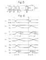
- Fig. 5 which is an equivalent circuit diagram of the memory-cell array MCA.
- the parasitic resistors and the parasitic capacitors are represented by the reference symbols R and C, respectively.
- Other members W + , W - and MC have already been explained before.
- the response time of the word line W is relatively long. To be specific, it takes a relatively long time for the word line W - to change from "H" (high) voltage level (selection status) of the word line W - to "L" (low) voltage level (non-selection status) thereof.
- the bit current, flowing through one memory cell which is situated in a condition changing from the selection status to the non-selection status is generated for a relatively long time.
- the first problem is that the access time for achieving the read operation, is considerably long, which means that high speed read operation cannot be expected. This is because, since the logic of one memory cell is maintained on one bit line for a relatively long time, the logic of the other memory which is going to be read from the sense amplifier, can not be detected quickly from the same bit line.
- the second problem is that the write operation cannot be achieved with a high degree of accuracy when a high speed write operation is conducted. In other words, a so-called write error, that is a "double write", is produced.
- Fig. 6 depicts waveforms of the voltage signal or the current signal appearing in the circuit shown in Fig. 4.
- row (a) depicts waveforms of the voltage signals appearing at the bases of the word drivers WDA and WDB (see Fig. 4).
- Row (b) depicts waveforms of the voltage signals appearing on the word lines WA - and WB - of the memory-cell arrays MCAA and MCAB (see Fig. 4), respectively.
- Row (c) depicts waveforms of voltage signals appearing on the bit lines BO and Bl (see Fig. 4).
- the stored logic of the last selected memory cell, in the memory-cell array MCAA is different from that of the newly selected memory cell, in the memory-cell array MCAB.
- the voltage level on the word line WA falls from the level "H” to the level “L”, because the memory-cell array MCAA changes from the selection status to the non-selection status.
- the change from the selection status to the non-selection status takes place very slowly. This is because, the voltage level on the word line WA - falls very slowly from the level "H” to the level "L”, due to the presence of the aforesaid parasitic capacitors C and parasitic resistors R, which exist along the word line WA - .
- the read operation becomes effective when the voltage difference between the bit lines BO and Bl exceeds a predetermined reference voltage (refer to the voltage " VR" in row (c) of Fig. 6).
- the access time for reading data can be defined by the time tl (refer to the row (c)).
- the identical read operation may also be achieved after the T 2 .
- the access time tl should be shortened.
- the time, required for discharging the electric charges on the word line WA should be shortened.
- a large hold current may be absorbed by the hold-current sources I H , so as to shorten said time tl which is required, as mentioned above, for discharging the electric charges on the word line WA .
- the best way to shorten the time tl is not by increasing the magnitude of the hold current, at least from an economical point of view. This is because, the non-selected memory--cell arrays waste too much hold current. The waste of the hold current will become very noticeable, if the semiconductor memory device is fabricated as a large capacity RAM (random access memory).
- the IIL memory circuit device of the present invention introduces therein a discharging means for discharging the electric charges stored in the parasitic capacitors C distributed along the word lines W_.
- Each of the word lines W - has at least one discharging means.
- the discharging means become operative only when the corresponding memory-cell array changes from the selection status to the non-selection status. Further, the electric charges, stored in one memory-cell array which is being changed from the selection status to the non-selection status, are absorbed via the discharging means with the aid of a constant-current source.
- the memory-cell array to be selected is switched at the time T 1 from the array MCAA to the array MCAB.
- the discharging currents I DA and I DB flowing respectively through the arrays MCAA and MCAB, change, as shown in row (d). Further, the transition from I DA to I DB (see row (d)) takes place after the occurrence of the transition from WA - to WB - (see row (b)). Therefore, the discharging current continues flowing even though the transition, from WA to WB has already been completed. As a result, the electric charges, stored in the parasitic capacitors C along the word line WA , are still absorbed as the discharging current by the constant-current source via the discharging means, even though the selection of the memory-cell array, from the array MCAA to the MCAB, has already been completed.
- the voltage level on the word line WA - changes from the level "H” to the level “L” faster, as shown in row (e), than that shown in row (b).
- the voltage difference between the bit lines BO and Bl exceeds the reference voltage ⁇ VR after the elapse of the time t2 (see row (f)) which occurs faster than the time tl (see row (c)). That is, a short access time (t2) for reading data is obtained.
- the above mentioned write error, or the double write can also be eliminated.
- the discharging means In each of the memory-cell arrays MCA, the discharging means should be located at a particular position or positions. If one discharging means is employed in each memory-cell array MCA, the discharging means should be located at the center of the array MCA, as shown in Fig. 7A. While, if a plurality of discharging means, for example three means, are employed in each memory-cell array MCA, these discharging means should be uniformly distributed along the array MCA, as shown in Fig. 7B. In Figs. 7A and 7B, the members MC are the memory cells, identical with those shown in Figs. 1, 4 and 5. The members DS represent the discharging members according to the present invention.
- the discharging means DS cooperate with one or more constant-current sources, but these are not illustrated in these figures.
- the arrangement, illustrated in Fig. 7A, is suitable for the construction of relatively small capacity RAM, while, the arrangement, illustrated in Fig. 7B, is suitable for the construction of relatively large capacity RAM.
- the discharging means DS acts as an irregular portion with respect to the adjacent memory cells MC.
- a continuity created along the successive memory cells, is broken by the irregular portion where the discharging means is located.
- the threshold current for writing data flowing through the memory cell which is located adjacent to the irregular portion, abnormally increases.
- the applicant of the present invention has already proposed a means for smoothing the irregular portion, called dummy cell (DC) in the Japanese patent application No. 56007/78, filed May 11, 1978.
- the dummy cell includes the injector (see region pl in Fig. 2) therein, as does the IIL memory cell, the threshold current, flowing through the adjacent memory cell, is shunted by the injector. Consequently, the increase of the threshold current can be suppressed.
- the dummy cell it is- preferable for the dummy cell to be formed with a pattern identical to the pattern of the memory cell.
- the discharging means comprised of the dummy cells (DC), are shown in Fig. 8.
- Each of the dummy cells DC is comprised of transistors which are identical to the transistors Ql, Q2 and Q3 for comprising each memory cell MC.
- the transitor Q3 may be substituted for a transitor which is identical to the transistor Q4 of the memory cell MC.
- the dummy cells DC do not conduct the read and write operation, it is not necessary to use two transistors, identical to the transistors Q3 and Q4 for storing data in the memory cell MC, simultaneously. Accordingly, either one of the transistors, identical to the transistors Q3 and Q4, can be employed, which transistor is always made conductive. Transistors, identical to the transistors Q5 and Q6, are not required in the cell DC.
- the dummy cells DC (DCA, DCB and so on) are connected to the constant-current source I C via respective junction members JC (JCA, JCB and so on) and respective discharging paths DP (DPA, DPB and so on).
- junction members JC is made active and supplies the discharging current therethrough back to the constant--current source I C , only when the corresponding memory-cell array is changed from the selection status to the non-selection status. In other words, the junction members JC discharge the electric charges selectively among one of the word lines W - , which word line changes from the selection status to the non-selection status.
- the junction member can be made of either a transistor, a diode, a resistor or a series connected diode and a resistor.
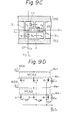
- Fig. 9A illustrates an equivalent circuit diagram of the dummy cell (DC) which cooperates with the diode d acting as the junction member (JC).
- the members represented by the symbols Q 1 , Q 2 , Q 3 ' DC, W , W - , DP, have already been explained.
- the diode d is comprised of a transistor, where the collector and the base of the transistor are shorted so as to obtain a function of a diode.
- the anode of the diode is connected to the word line W and the cathode thereof is connected to the discharging path DP which leads to the constant-current source I C .
- identical diodes d of other memory-cell arrays (not shown in Fig. 9A) are also connected, at their anodes, to respective word lines (W ), while, the cathodes of diodes are commonly connected to the single discharging path DP. Accordingly, one of the diodes d, which the diode d is connected to the word line W- changing from the selection status ("H" level) to the non-selection status, can be conductive.
- Fig. 9B is a cross sectional view of basic layout for constructing the circuit diagram shown in Fig. 9A.
- Members, represented by the symbols pl through p4, are p-type regions, and members, represented by the symbols nl through n5, are n-type regions.
- the hatching regions represent isolation regions.
- Fig. 9C is a plan view of actual layout for constructing the circuit diagram shown in Fig. 9A.
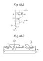
- Fig. 10A illustrates an equivalent circuit diagram of the dummy cell (DC) which cooperates with the resistor r acting as the junction member (JC).
- One end of the resistor r is connected to the word line W and the other end thereof is connected to the discharging path DP.
- identical resistors r of other memory-cell arrays (not shown in Fig. 10A) are also connected, at each one end thereof, to respective word lines (W ), while, each other end thereof, is connected to the discharging path DP.
- the resistance value of each resistor r should be determined in such a manner that the discharging current I does not reversely flow toward the non-selected word lines W - .
- Fig. 10B is a cross sectional view of basic layout for constructing the circuit diagram shown in Fig. 10A.
- Fig. 10C is a plan view of actual layout for constructing the circuit diagram shown in Fig. 10A.
- the junction member, comprised of the resistor r has an advantage, when compared to the junction member which is comprised of the diode d (Fig. 9A), in that the discharging current I D , flowing through the resistor r, can continue flowing for a longer time than the time during which the discharging current I D flows through the diode d.
- the electric charges, stored in the parasitic capacitors C can fully be absorbed through the resistor r.
- the diode d can no longer be conductive and cuts off the discharging current I D , soon after when the diode d is reversely biased.
- the junction member, comprised of the diode d (Fig.
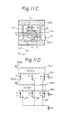
- Fig. 11A illustrates an equivalent circuit diagram of the dummy cell (DC) which cooperates with the series connected diode d and resistor r, both acting as the junction member JC.
- the anode of the diode d is connected to the word line W - , the cathode thereof is connected to one end of the resistor r, the other end thereof is connected to the discharging path DP.
- Fig. 11D identical pairs of series connected diodes d and resistors r of other memory-cell arrays (not shown in Fig.
- Fig. 11A is also connected between respective word lines (W - ) and the common discharging path DP.
- Fig. 11B is a cross sectional view of basic layout for constructing the circuit diagram shown in Fig. 11A.
- Fig. 11C is a plan view of actual layout for constructing the circuit diagram shown in Fig. 11A.
- the junction member JC can also be fabricated by a transistor.
- Fig. 12 illustrates an equivalent circuit diagram of the dummy cell (DC) which cooperates with the transistor acting as the junction member (JC).
- DC dummy cell
- JC junction member
- identical transistors Q7 of other memory-cell arrays are also connected, at-their collectors, to respective word lines W and also connected, at their emitters, to the common discharging path DP.
- the voltage level, at the base of the transistor Q7 should be proportional to the voltage level developed at a suitable position in the dummy cell DC, so far as the voltage level varies in accordance with the variation of the voltage level on the word line W .
- the base of the transistor Q7 is connected to the collector of the aforesaid transistor Q3.
- the function of the transistor Q7 is substantially the same as that of the diode d shown in Fig. 9A.
- the location of the transistor Q7 may be the same as that of the transistor Q5 to be positioned in the IIL memory cell MC (see Fig. I).
- the location of each of the aforesaid diodes d, resistors r and pairs of series connected diodes d and resistors r may be the same as that of the transistor Q5 positioned in the IIL memory cell MC (see Fig. 1).
- a transistor for comprising the aforementioned hold-current source IH at the position where the transistor Q6 is positioned in the IIL memory cell MC.
- Fig. 13A is an equivalent circuit diagram of the dummy cell DC, the junction member JC which is comprised of the transistor Q7 (see oFig. 12) and the hold-current sourse I H which is comprised of a transistor Q8.
- junction member JC is not limited to the transistor Q7, but is also applicable with respect to the diode d (see Fig. 9A), the resistor r (see Fig. 10A) or the series connected diode d and resistor r (see Fig. 11A).
- Fig. 13B is a cross sectional view of a basic layout for constructing the circuit diagram shown in Fig. 13A.
- Fig. 13C is a plan view of an actual layout for constructing the circuit diagram shown in Fig. 13A.
- the IIL memory circuit device has a capability for achieving high speed read and write operations and also produces no write error, that is the "double write".
Landscapes
- Engineering & Computer Science (AREA)
- Microelectronics & Electronic Packaging (AREA)
- Computer Hardware Design (AREA)
- Power Engineering (AREA)
- Semiconductor Memories (AREA)
- Static Random-Access Memory (AREA)
Applications Claiming Priority (4)
| Application Number | Priority Date | Filing Date | Title |
|---|---|---|---|
| JP154025/79 | 1979-11-28 | ||
| JP54154025A JPS5843835B2 (ja) | 1979-11-28 | 1979-11-28 | 半導体記憶装置 |
| JP54155340A JPS5838871B2 (ja) | 1979-11-30 | 1979-11-30 | 半導体記憶装置 |
| JP155340/79 | 1979-11-30 |
Publications (3)
| Publication Number | Publication Date |
|---|---|
| EP0030422A2 true EP0030422A2 (fr) | 1981-06-17 |
| EP0030422A3 EP0030422A3 (en) | 1983-06-08 |
| EP0030422B1 EP0030422B1 (fr) | 1987-05-27 |
Family
ID=26482456
Family Applications (1)
| Application Number | Title | Priority Date | Filing Date |
|---|---|---|---|
| EP80304083A Expired EP0030422B1 (fr) | 1979-11-28 | 1980-11-13 | Dispositif de mémoire à semi-conducteurs |
Country Status (5)
| Country | Link |
|---|---|
| US (1) | US4374431A (fr) |
| EP (1) | EP0030422B1 (fr) |
| CA (1) | CA1175143A (fr) |
| DE (1) | DE3071976D1 (fr) |
| IE (1) | IE52801B1 (fr) |
Cited By (3)
| Publication number | Priority date | Publication date | Assignee | Title |
|---|---|---|---|---|
| GB2117592A (en) * | 1982-03-29 | 1983-10-12 | Fairchild Camera Instr Co | Word line cell discharge current bypass |
| EP0071470A3 (en) * | 1981-07-29 | 1984-12-27 | Fujitsu Limited | Semiconductor memory devices including line driver circuits |
| EP0283019A3 (en) * | 1987-03-17 | 1990-01-10 | Sony Corporation | Semiconductor memory device |
Families Citing this family (3)
| Publication number | Priority date | Publication date | Assignee | Title |
|---|---|---|---|---|
| JPS58159294A (ja) * | 1982-03-17 | 1983-09-21 | Hitachi Ltd | 半導体記憶装置 |
| JPS60177724A (ja) * | 1984-02-24 | 1985-09-11 | Hitachi Ltd | 論理回路 |
| US4813017A (en) * | 1985-10-28 | 1989-03-14 | International Business Machines Corportion | Semiconductor memory device and array |
Family Cites Families (4)
| Publication number | Priority date | Publication date | Assignee | Title |
|---|---|---|---|---|
| JPS5341968A (en) * | 1976-09-29 | 1978-04-15 | Hitachi Ltd | Semiconductor circuit |
| JPS54147741A (en) * | 1978-05-11 | 1979-11-19 | Fujitsu Ltd | Semiconductor integrated circuit unit |
| EP0005601B1 (fr) * | 1978-05-11 | 1983-03-02 | Nippon Telegraph and Telephone Public Corporation | Circuit semiconducteur intégré à mémoire |
| US4168490A (en) * | 1978-06-26 | 1979-09-18 | Fairchild Camera And Instrument Corporation | Addressable word line pull-down circuit |
-
1980
- 1980-11-13 EP EP80304083A patent/EP0030422B1/fr not_active Expired
- 1980-11-13 DE DE8080304083T patent/DE3071976D1/de not_active Expired
- 1980-11-18 IE IE2393/80A patent/IE52801B1/en unknown
- 1980-11-21 CA CA000365235A patent/CA1175143A/fr not_active Expired
- 1980-11-26 US US06/210,678 patent/US4374431A/en not_active Expired - Lifetime
Cited By (3)
| Publication number | Priority date | Publication date | Assignee | Title |
|---|---|---|---|---|
| EP0071470A3 (en) * | 1981-07-29 | 1984-12-27 | Fujitsu Limited | Semiconductor memory devices including line driver circuits |
| GB2117592A (en) * | 1982-03-29 | 1983-10-12 | Fairchild Camera Instr Co | Word line cell discharge current bypass |
| EP0283019A3 (en) * | 1987-03-17 | 1990-01-10 | Sony Corporation | Semiconductor memory device |
Also Published As
| Publication number | Publication date |
|---|---|
| IE52801B1 (en) | 1988-03-16 |
| DE3071976D1 (en) | 1987-07-02 |
| CA1175143A (fr) | 1984-09-25 |
| EP0030422B1 (fr) | 1987-05-27 |
| US4374431A (en) | 1983-02-15 |
| EP0030422A3 (en) | 1983-06-08 |
| IE802393L (en) | 1981-05-28 |
Similar Documents
| Publication | Publication Date | Title |
|---|---|---|
| US3815106A (en) | Flip-flop memory cell arrangement | |
| US4090254A (en) | Charge injector transistor memory | |
| US3729719A (en) | Stored charge storage cell using a non latching scr type device | |
| US4322820A (en) | Semiconductor integrated circuit device | |
| EP0130793B1 (fr) | Dispositif de mémoire semi-conductrice | |
| US3863229A (en) | Scr (or scs) memory array with internal and external load resistors | |
| US4112511A (en) | Four transistor static bipolar memory cell using merged transistors | |
| US4663741A (en) | Strobed access semiconductor memory system | |
| US4374431A (en) | I2 L Semiconductor memory circuit device | |
| EP0028157B1 (fr) | Circuit intégré semiconducteur à mémoire à logique d'injection intégrée | |
| US3603820A (en) | Bistable device storage cell | |
| US4122548A (en) | Memory storage array with restore circuit | |
| US4122542A (en) | Memory array | |
| JPH0217876B2 (fr) | ||
| US3820086A (en) | Read only memory(rom)superimposed on read/write memory(ram) | |
| EP0023408B1 (fr) | Mémoire à semi-conducteurs comprenant des cellules intégrées à injection logique | |
| EP0006753B1 (fr) | Circuit intégré à semi-conducteur | |
| EP0020769B1 (fr) | Systeme de memoire a semi-conducteur | |
| EP0057556B1 (fr) | Dispositif de mémoire statique semi-conductrice | |
| KR910002502B1 (ko) | 복수개의 가변 클램프형 메모리 셀을 구비한 메모리 회로 | |
| US4589096A (en) | IIL semiconductor memory including arrangement for preventing information loss during read-out | |
| EP0080351B1 (fr) | Transistors à émetteurs multiples dans des dispositifs de mémoires sémi-conductrices | |
| JPH0529993B2 (fr) | ||
| US4313177A (en) | Storage cell simulation for generating a reference voltage for semiconductor stores in mtl technology | |
| EP0037734B1 (fr) | Circuit intégré de mémoire à semi-conducteurset dispositif de mémoire utilisant ces circuits |
Legal Events
| Date | Code | Title | Description |
|---|---|---|---|
| PUAI | Public reference made under article 153(3) epc to a published international application that has entered the european phase |
Free format text: ORIGINAL CODE: 0009012 |
|
| 17P | Request for examination filed |
Effective date: 19801121 |
|
| AK | Designated contracting states |
Designated state(s): DE FR GB NL |
|
| PUAL | Search report despatched |
Free format text: ORIGINAL CODE: 0009013 |
|
| AK | Designated contracting states |
Designated state(s): DE FR GB NL |
|
| ITF | It: translation for a ep patent filed | ||
| GRAA | (expected) grant |
Free format text: ORIGINAL CODE: 0009210 |
|
| AK | Designated contracting states |
Kind code of ref document: B1 Designated state(s): DE FR GB NL |
|
| PG25 | Lapsed in a contracting state [announced via postgrant information from national office to epo] |
Ref country code: NL Effective date: 19870527 |
|
| REF | Corresponds to: |
Ref document number: 3071976 Country of ref document: DE Date of ref document: 19870702 |
|
| ET | Fr: translation filed | ||
| NLV1 | Nl: lapsed or annulled due to failure to fulfill the requirements of art. 29p and 29m of the patents act | ||
| PLBE | No opposition filed within time limit |
Free format text: ORIGINAL CODE: 0009261 |
|
| STAA | Information on the status of an ep patent application or granted ep patent |
Free format text: STATUS: NO OPPOSITION FILED WITHIN TIME LIMIT |
|
| 26N | No opposition filed | ||
| PGFP | Annual fee paid to national office [announced via postgrant information from national office to epo] |
Ref country code: FR Payment date: 19891129 Year of fee payment: 10 |
|
| PGFP | Annual fee paid to national office [announced via postgrant information from national office to epo] |
Ref country code: GB Payment date: 19891130 Year of fee payment: 10 |
|
| PGFP | Annual fee paid to national office [announced via postgrant information from national office to epo] |
Ref country code: DE Payment date: 19900128 Year of fee payment: 10 |
|
| PG25 | Lapsed in a contracting state [announced via postgrant information from national office to epo] |
Ref country code: GB Effective date: 19901113 |
|
| GBPC | Gb: european patent ceased through non-payment of renewal fee | ||
| PG25 | Lapsed in a contracting state [announced via postgrant information from national office to epo] |
Ref country code: FR Effective date: 19910731 |
|
| PG25 | Lapsed in a contracting state [announced via postgrant information from national office to epo] |
Ref country code: DE Effective date: 19910801 |
|
| REG | Reference to a national code |
Ref country code: FR Ref legal event code: ST |