EP0030612A2 - Verfahren zur Doppelfehlerkorrektur in einem Datenspeichergerät und Datenspeichergerät - Google Patents
Verfahren zur Doppelfehlerkorrektur in einem Datenspeichergerät und Datenspeichergerät Download PDFInfo
- Publication number
- EP0030612A2 EP0030612A2 EP80106632A EP80106632A EP0030612A2 EP 0030612 A2 EP0030612 A2 EP 0030612A2 EP 80106632 A EP80106632 A EP 80106632A EP 80106632 A EP80106632 A EP 80106632A EP 0030612 A2 EP0030612 A2 EP 0030612A2
- Authority
- EP
- European Patent Office
- Prior art keywords
- syndrome
- error
- ecc
- code
- bit
- Prior art date
- Legal status (The legal status is an assumption and is not a legal conclusion. Google has not performed a legal analysis and makes no representation as to the accuracy of the status listed.)
- Granted
Links
Images
Classifications
-
- G—PHYSICS
- G06—COMPUTING OR CALCULATING; COUNTING
- G06F—ELECTRIC DIGITAL DATA PROCESSING
- G06F11/00—Error detection; Error correction; Monitoring
- G06F11/07—Responding to the occurrence of a fault, e.g. fault tolerance
- G06F11/08—Error detection or correction by redundancy in data representation, e.g. by using checking codes
- G06F11/10—Adding special bits or symbols to the coded information, e.g. parity check, casting out 9's or 11's
- G06F11/1008—Adding special bits or symbols to the coded information, e.g. parity check, casting out 9's or 11's in individual solid state devices
- G06F11/1048—Adding special bits or symbols to the coded information, e.g. parity check, casting out 9's or 11's in individual solid state devices using arrangements adapted for a specific error detection or correction feature
-
- G—PHYSICS
- G06—COMPUTING OR CALCULATING; COUNTING
- G06F—ELECTRIC DIGITAL DATA PROCESSING
- G06F11/00—Error detection; Error correction; Monitoring
- G06F11/07—Responding to the occurrence of a fault, e.g. fault tolerance
- G06F11/08—Error detection or correction by redundancy in data representation, e.g. by using checking codes
- G06F11/10—Adding special bits or symbols to the coded information, e.g. parity check, casting out 9's or 11's
- G06F11/1008—Adding special bits or symbols to the coded information, e.g. parity check, casting out 9's or 11's in individual solid state devices
- G06F11/1012—Adding special bits or symbols to the coded information, e.g. parity check, casting out 9's or 11's in individual solid state devices using codes or arrangements adapted for a specific type of error
- G06F11/1024—Identification of the type of error
Definitions
- the present invention relates to augmenting the correction capability of error correction mechanisms in data storage apparatus.
- Errors in data stored in memories can be said to have two major causes.
- One cause is the intrinsic physical failure of memory components which usually produces a permanent or "hard” error.
- the other cause is non-destructive environmental phenomena which causes errors which for the most part are transient, intermittent or "soft" errors.
- soft errors due to external or environmental interference are more prevalent than hard errors resulting from component failures.
- Laboratory evidence shows that the alpha-particle induced failure rate alone is one to two orders of magnitude higher than the memory chips basic intrinsic failure rate.
- alpha-induced failure rates usually are higher at higher chip densities indicating that soft errors will be of even greater significance in the future.
- Error correcting codes have traditionally been used in improving reliability in the storage area of computers.
- the most widely used codes are single error correcting and double error detecting SEC/DED codes.
- This class of codes is most effective in memory systems organized on a one bit per card, chip or module basis. With the one bit per card, chip or module organization, multiple errors caused by the failure of a card, chip or module will only cause a single bit error in any encoded data word.
- the mapping of component failures into single bit errors has resulted in the use of delayed system maintenance procedures that allow component failures to accumulate to some threshold level before they are repaired or replaced. This is done under the assumption that the errors caused by the component failures will be corrected by the SEC/DED error correction system.
- the memory location where the data word was stored is then checked using ancillary correction means to locate stuck bits in the data word location.
- a syndrome is thereafter generated for a data word with stuck bits in the positions located by the ancillary process. If this syndrome matches the stored syndrome the word is corrected by inverting the data bits in the stored data word at the stuck bit positions. If it doesn't the publication suggests that the actual bits among the faulty bits in error can be determined by "iterative partitioning" of the faulty bits and determining the error syndrome for each portion.
- the present invention provides data storage apparatus comprising a storage array having an input/output interface including a code based error detecting and correcting mechanism (ECC) and an ancilliary array test mechanism (ATM) characterised in that, the interface includes means to store both data detected to be in error but uncorrectable by the ECC and the corresponding syndrome, means to generate a syndrome within the ECC code for errors determined by the ATM, and means to combine the stored and generated syndrome to generate a composite syndrome for correction of the stored data in error by the ECC if the generated composite syndrome is valid within the ECC code for this purpose.
- ECC code based error detecting and correcting mechanism
- ATM ancilliary array test mechanism
- the present invention provides data storage apparatus including a storage array 12 coupled to the outside world through an interface which includes two error mechanisms, the one being a code based error detecting and correcting mechanism (ECC), the other being an array testing mechanism (ATM) which is ancilliary in the sense that, should the ECC suffice, the ATM is not used.
- ECC code based error detecting and correcting mechanism
- ATM array testing mechanism
- the data and the error syndrome are saved in the interface, the ATM is invoked to determine hard errors in the storage array and, if such detected errors are determined by test to be of a number compatible with the detecting capacity of the ECC, a syndrome is generated for the detected errors, which syndrome is combined with the stored syndrome, tested for compatibility with the ECC and used by the ECC for correction.
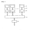
- the storage array 12 is in the form of 72 cards 100 each carrying a plurality of bit storage positions 101 and associated accessing controls 102, the array functioning to access one bit position per card and to transfer data between the cards and an internal register 103 which in turn communicates with the storage data register 14 which appears in both FIGS. 1 and 3 and comprises the array side of the input/output interface for the apparatus.
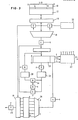
- the interface is shown in Figure 3.
- a word 10 accessed from the array 12 into storage data register 14, is transmitted to an output register 16 and to a syndrome generator 18.
- the syndrome generator 18 generates a.syndrome which is fed to an associative store 20.
- the associative store 20 is a 73 word memory storing each of the syndromes for a single bit in error at any one of the 72 bit locations of the word plus the syndrome for no bits in the word in error.
- Stored along with the syndrome is a 7 bit number identifying the position of the bit error in binary sequence.
- the syndrome generator 16 produces a syndrome of all zeros, or in other words, a syndrome which indicates no bits in the accessed word are in error.
- Stored along with the syndrome in associative store with the all zero syndrome would be a string of seven additional zeros indicating that there is no error.
- This string of seven zeros is fed to a controller 22 which then generates a gate signal for gate 24 allowing the error free data word stored in register 16 to be transmitted to the processor.
- the syndrome generator generates a syndrome S h that would indicate that a single bit error has occurred.
- a syndrome generator 18 generates a syndrome S h that does not match with any of the 73 syndromes stored in the associative store 20.
- Associative store 20 then generates a no compare signal C and feeds it to the error control 22.
- the error control 22 Upon receipt of a no compare signal, the error control 22 stores the uncorrectable error syndrome in the SU register 28. It also transmits the test words P 1 , P 2 and P 3 from the store 20 to the storage data register 14 for reading into the flawed storage location 10.
- the syndrome generator 18 generates the appropriate one of the syndromes S 1 , S 2 and S 3 when one of the syndromes S 1 , S 2 , S 3 is received by the associative store 20 from the syndrome generator 18 the associative store generates a compare or a no compare signal and with a compare signal, an error location. If there is three no compare signals, the error control terminates the error correction process and indicates an uncorrectable error condition exists. Likewise, if the compare signals generated for two or more of the syndromes S 1 , S 2 and S point to different bits in error the controller 20 terminates the error correction process and indicates a true uncorrectable error condition exists.
- the controller loads the syndrome Sh for the location identified by the three syndromes into the S register 32 and then feeds the contents of both registers 28 and 32 into Exclusive OR circuit 34 to perform an Exclusive OR function of the two syndromes S u and S he
- the output (composite syndrome) S ⁇ of the Exclusive OR circuit 34 is fed back into the associative store 20 to determine if it matches any of the syndromes stored in the associative store 20.
- a no compare signal is generated by the associative store 20 and fed to the controller 22 which then terminates the error correction process and indicates a true uncorrectable error condition exists. If it does, the error controller receives a compare signal and the location ⁇ of the bit in error is transmitted to the decoder from the store in 7 bit binary notation to invert the data in bit location of the register 16.
- the syndrome S h is then fed from register 32 to the store 20 which feeds the location of bit h to the decoder 26..
- the decoder 26 then instructs the bit inverter 26 to invert the bit h.
- the data stored in register 16 is now correct and the controller 22 opens the gate 24 and transmits the data to the processor.
- Relationship (1) can be used to correct those double bit errors made up of one hard error and one soft error.
- the ECC hardware detects an uncorrectable error condition in an encoded data word stored in some location in memory, that encoded data word is saved at 16 along with the syndrome SU , at 28 generated by the ECC hardware from that encoded word.
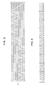
- test patterns shown in Figure 4 and stored at 30 are then used to locate the bit position of the hard error by interrogating the memory location. It will be noted that each pattern is a valid word (data plus check bits) within the code and that each bit position, when exercised by P 1 followed by P 2 followed by P 3 will be set to 1 and 0 so that either form of hard error will show up either once or twice, but not three times.
- Each of the patterns P 1 , P 2 and P 3 is written into the location and read out of the location. Syndromes S 1 , S 2 and S are generated from the read out data. Each of these three syndromes is decoded 5 by the ECC circuitry to determine the locations of any bits in error.
- the correcting scheme is terminated 6 and a true uncorrectable error condition is indicated.
- the final consistency test is checking syndrome S ⁇ to determine if it is a valid single error syndrome. If it is, the bit position ⁇ of the soft error is known and the stored word can be corrected by inverting the bits at locations ⁇ and h. If not, an indication is given that a true uncorrectable error condition exists.
Landscapes
- Engineering & Computer Science (AREA)
- Theoretical Computer Science (AREA)
- Quality & Reliability (AREA)
- Physics & Mathematics (AREA)
- General Engineering & Computer Science (AREA)
- General Physics & Mathematics (AREA)
- Detection And Correction Of Errors (AREA)
- Error Detection And Correction (AREA)
- Techniques For Improving Reliability Of Storages (AREA)
Applications Claiming Priority (2)
| Application Number | Priority Date | Filing Date | Title |
|---|---|---|---|
| US06/103,633 US4319357A (en) | 1979-12-14 | 1979-12-14 | Double error correction using single error correcting code |
| US103633 | 1998-06-23 |
Publications (3)
| Publication Number | Publication Date |
|---|---|
| EP0030612A2 true EP0030612A2 (de) | 1981-06-24 |
| EP0030612A3 EP0030612A3 (en) | 1982-02-10 |
| EP0030612B1 EP0030612B1 (de) | 1984-08-08 |
Family
ID=22296201
Family Applications (1)
| Application Number | Title | Priority Date | Filing Date |
|---|---|---|---|
| EP80106632A Expired EP0030612B1 (de) | 1979-12-14 | 1980-10-29 | Verfahren zur Doppelfehlerkorrektur in einem Datenspeichergerät und Datenspeichergerät |
Country Status (4)
| Country | Link |
|---|---|
| US (1) | US4319357A (de) |
| EP (1) | EP0030612B1 (de) |
| JP (1) | JPS6047625B2 (de) |
| DE (1) | DE3068895D1 (de) |
Families Citing this family (33)
| Publication number | Priority date | Publication date | Assignee | Title |
|---|---|---|---|---|
| JPS598852B2 (ja) * | 1979-07-30 | 1984-02-28 | 富士通株式会社 | エラ−処理方式 |
| US4464753A (en) * | 1981-12-30 | 1984-08-07 | International Business Machines Corporation | Two bit symbol SEC/DED code |
| US4531213A (en) * | 1982-03-03 | 1985-07-23 | Sperry Corporation | Memory through checking system with comparison of data word parity before and after ECC processing |
| US4509172A (en) * | 1982-09-28 | 1985-04-02 | International Business Machines Corporation | Double error correction - triple error detection code |
| US4523314A (en) * | 1983-02-07 | 1985-06-11 | Sperry Corporation | Read error occurrence detector for error checking and correcting system |
| DE3473365D1 (en) * | 1984-05-26 | 1988-09-15 | Honeywell Bull Spa | Single error correction circuit for system memory |
| DE3482509D1 (de) * | 1984-12-28 | 1990-07-19 | Ibm | Geraet zum korrigieren von fehlern in speichern. |
| US4661955A (en) * | 1985-01-18 | 1987-04-28 | Ibm Corporation | Extended error correction for package error correction codes |
| US4780809A (en) * | 1986-08-08 | 1988-10-25 | Amdahl Corporation | Apparatus for storing data with deferred uncorrectable error reporting |
| US4817095A (en) * | 1987-05-15 | 1989-03-28 | Digital Equipment Corporation | Byte write error code method and apparatus |
| US5014273A (en) * | 1989-01-27 | 1991-05-07 | Digital Equipment Corporation | Bad data algorithm |
| WO1992012483A1 (en) * | 1991-01-08 | 1992-07-23 | The Dsp Group, Inc. | Data reception technique |
| US5426652A (en) * | 1991-01-08 | 1995-06-20 | The Dsp Group Inc. | Data reception technique |
| US5418796A (en) * | 1991-03-26 | 1995-05-23 | International Business Machines Corporation | Synergistic multiple bit error correction for memory of array chips |
| US5195098A (en) * | 1991-05-10 | 1993-03-16 | Echelon Corporation | Binary data error correction using hint signal |
| US5491700A (en) * | 1993-10-01 | 1996-02-13 | Pacific Communication Sciences, Inc. | Method and apparatus for code error correction using an ordered syndrome and error correction lookup table |
| US5774481A (en) * | 1995-03-31 | 1998-06-30 | International Business Machines Corporation | Reduced gate error detection and correction circuit |
| US5920580A (en) * | 1996-03-11 | 1999-07-06 | Integrated Device Technology, Inc. | Multiple error detection in error detection correction circuits |
| JP2820124B2 (ja) * | 1996-06-27 | 1998-11-05 | 日本電気株式会社 | 主記憶装置 |
| US6556984B1 (en) | 1999-01-19 | 2003-04-29 | International Business Machines Corporation | Hierarchical string matching using multi-path dynamic programming |
| US7320100B2 (en) * | 2003-05-20 | 2008-01-15 | Cray Inc. | Apparatus and method for memory with bit swapping on the fly and testing |
| US7184916B2 (en) * | 2003-05-20 | 2007-02-27 | Cray Inc. | Apparatus and method for testing memory cards |
| US7171591B2 (en) * | 2003-12-23 | 2007-01-30 | International Business Machines Corporation | Method and apparatus for encoding special uncorrectable errors in an error correction code |
| EP1560118A1 (de) * | 2004-01-27 | 2005-08-03 | Infineon Technologies AG | Verfahren und Vorrichtung zur Erkennung und Korrektur von Fehlern |
| US7653862B2 (en) * | 2005-06-15 | 2010-01-26 | Hitachi Global Storage Technologies Netherlands B.V. | Error detection and correction for encoded data |
| DE102006003146B4 (de) * | 2006-01-23 | 2016-05-12 | Infineon Technologies Ag | Vorrichtung und Verfahren zum Auslesen eines Datenwortes und Vorrichtung und Verfahren zum Speichern eines Datenblocks |
| US7506226B2 (en) * | 2006-05-23 | 2009-03-17 | Micron Technology, Inc. | System and method for more efficiently using error correction codes to facilitate memory device testing |
| US7747913B2 (en) * | 2007-08-03 | 2010-06-29 | Intel Corporation | Correcting intermittent errors in data storage structures |
| TW200947450A (en) * | 2008-05-09 | 2009-11-16 | A Data Technology Co Ltd | Storage system capable of data recovery and method thereof |
| RU2450332C1 (ru) * | 2011-01-27 | 2012-05-10 | Межрегиональное общественное учреждение "Институт инженерной физики" | Устройство хранения информации с обнаружением одиночных и двойных ошибок |
| FR3044817B1 (fr) * | 2015-12-02 | 2017-12-22 | St Microelectronics Rousset | Procede de gestion d'une ligne de bits defectueuse du plan memoire d'une memoire non volatile et dispositif de memoire correspondant |
| RU2659479C1 (ru) * | 2017-06-01 | 2018-07-02 | Межрегиональное общественное учреждение "Институт инженерной физики" | Устройство хранения и передачи данных с обнаружением одиночных и двойных ошибок |
| KR102453437B1 (ko) | 2018-01-25 | 2022-10-12 | 삼성전자주식회사 | 반도체 메모리 장치, 이를 포함하는 메모리 시스템 및 반도체 메모리 장치의 동작 방법 |
Family Cites Families (9)
| Publication number | Priority date | Publication date | Assignee | Title |
|---|---|---|---|---|
| US3656107A (en) * | 1970-10-23 | 1972-04-11 | Ibm | Automatic double error detection and correction apparatus |
| DE2134529A1 (de) * | 1971-07-10 | 1973-01-25 | Ibm Deutschland | Verfahren zur fehlererkennung und -korrektur in aus dem speicher einer programmgesteuerten datenverarbeitungsanlage ausgelesenen informationswoertern |
| US4107652A (en) * | 1975-12-27 | 1978-08-15 | Fujitsu Limited | Error correcting and controlling system |
| JPS5381036A (en) * | 1976-12-27 | 1978-07-18 | Hitachi Ltd | Error correction-detection system |
| US4100403A (en) * | 1977-04-25 | 1978-07-11 | International Business Machines Corporation | Method and means for discriminating between systematic and noise-induced error in data extracted from word organized memory arrays |
| US4139148A (en) * | 1977-08-25 | 1979-02-13 | Sperry Rand Corporation | Double bit error correction using single bit error correction, double bit error detection logic and syndrome bit memory |
| US4209846A (en) * | 1977-12-02 | 1980-06-24 | Sperry Corporation | Memory error logger which sorts transient errors from solid errors |
| US4163147A (en) * | 1978-01-20 | 1979-07-31 | Sperry Rand Corporation | Double bit error correction using double bit complementing |
| DE2838005C2 (de) * | 1978-08-31 | 1980-08-28 | Siemens Ag, 1000 Berlin Und 8000 Muenchen | Verfahren und Einrichtung zur Korrektur von 2-Bit-FehIern in Codewörtern |
-
1979
- 1979-12-14 US US06/103,633 patent/US4319357A/en not_active Expired - Lifetime
-
1980
- 1980-10-06 JP JP55138883A patent/JPS6047625B2/ja not_active Expired
- 1980-10-29 DE DE8080106632T patent/DE3068895D1/de not_active Expired
- 1980-10-29 EP EP80106632A patent/EP0030612B1/de not_active Expired
Also Published As
| Publication number | Publication date |
|---|---|
| EP0030612B1 (de) | 1984-08-08 |
| DE3068895D1 (en) | 1984-09-13 |
| JPS6047625B2 (ja) | 1985-10-22 |
| JPS5687300A (en) | 1981-07-15 |
| EP0030612A3 (en) | 1982-02-10 |
| US4319357A (en) | 1982-03-09 |
Similar Documents
| Publication | Publication Date | Title |
|---|---|---|
| EP0030612B1 (de) | Verfahren zur Doppelfehlerkorrektur in einem Datenspeichergerät und Datenspeichergerät | |
| US4604751A (en) | Error logging memory system for avoiding miscorrection of triple errors | |
| US5619642A (en) | Fault tolerant memory system which utilizes data from a shadow memory device upon the detection of erroneous data in a main memory device | |
| US6067656A (en) | Method and apparatus for detecting soft errors in content addressable memory arrays | |
| US4654847A (en) | Apparatus for automatically correcting erroneous data and for storing the corrected data in a common pool alternate memory array | |
| US6018817A (en) | Error correcting code retrofit method and apparatus for multiple memory configurations | |
| KR100331139B1 (ko) | 에러 위치지정 코드를 사용하여 멀티레벨 셀 메모리를 정정하는방법 및 장치 | |
| US5663969A (en) | Parity-based error detection in a memory controller | |
| EP0139124A2 (de) | Vorrichtung und Verfahren zur automatischen Korrektur eines doppelten Hardbitfehlers im Speicher einer Datenverarbeitungsanlage und zur Sicherstellung, dass der genannte Fehler sich nicht mehr wiederholt | |
| JP4071940B2 (ja) | メモリ設計のための共有式誤り訂正 | |
| US6754858B2 (en) | SDRAM address error detection method and apparatus | |
| KR920002575B1 (ko) | 바이트 기입 에러코드 방법 및 장치 | |
| US4506364A (en) | Memory address permutation apparatus | |
| US4523314A (en) | Read error occurrence detector for error checking and correcting system | |
| EP0041999A4 (de) | System und verfahren für selbstkorrigierende speicher. | |
| EP0265639A2 (de) | Ausfallerkennung von Fehlerprüfungs- und -korrekturschaltung | |
| EP0242595B1 (de) | Fehlererkennung unter Verwendung von Paritätsprüfung mit veränderlichem Feld | |
| US20030140300A1 (en) | (146,130) error correction code utilizing address information | |
| EP0186719A1 (de) | Gerät zum Korrigieren von Fehlern in Speichern | |
| EP0037705A1 (de) | Fehlerkorrekturspeichersystem | |
| EP0281740B1 (de) | Speicher und deren Prüfung | |
| US5751745A (en) | Memory implemented error detection and correction code with address parity bits | |
| US5357521A (en) | Address sensitive memory testing | |
| US5761221A (en) | Memory implemented error detection and correction code using memory modules | |
| US7181655B2 (en) | Method and circuit arrangement for memory error processing |
Legal Events
| Date | Code | Title | Description |
|---|---|---|---|
| PUAI | Public reference made under article 153(3) epc to a published international application that has entered the european phase |
Free format text: ORIGINAL CODE: 0009012 |
|
| AK | Designated contracting states |
Designated state(s): DE FR GB |
|
| PUAL | Search report despatched |
Free format text: ORIGINAL CODE: 0009013 |
|
| AK | Designated contracting states |
Designated state(s): DE FR GB |
|
| 17P | Request for examination filed |
Effective date: 19820225 |
|
| GRAA | (expected) grant |
Free format text: ORIGINAL CODE: 0009210 |
|
| AK | Designated contracting states |
Designated state(s): DE FR GB |
|
| REF | Corresponds to: |
Ref document number: 3068895 Country of ref document: DE Date of ref document: 19840913 |
|
| ET | Fr: translation filed | ||
| PLBE | No opposition filed within time limit |
Free format text: ORIGINAL CODE: 0009261 |
|
| STAA | Information on the status of an ep patent application or granted ep patent |
Free format text: STATUS: NO OPPOSITION FILED WITHIN TIME LIMIT |
|
| 26N | No opposition filed | ||
| PGFP | Annual fee paid to national office [announced via postgrant information from national office to epo] |
Ref country code: GB Payment date: 19920925 Year of fee payment: 13 |
|
| PGFP | Annual fee paid to national office [announced via postgrant information from national office to epo] |
Ref country code: FR Payment date: 19920928 Year of fee payment: 13 |
|
| PGFP | Annual fee paid to national office [announced via postgrant information from national office to epo] |
Ref country code: DE Payment date: 19921027 Year of fee payment: 13 |
|
| PG25 | Lapsed in a contracting state [announced via postgrant information from national office to epo] |
Ref country code: GB Effective date: 19931029 |
|
| GBPC | Gb: european patent ceased through non-payment of renewal fee |
Effective date: 19931029 |
|
| PG25 | Lapsed in a contracting state [announced via postgrant information from national office to epo] |
Ref country code: FR Effective date: 19940630 |
|
| PG25 | Lapsed in a contracting state [announced via postgrant information from national office to epo] |
Ref country code: DE Effective date: 19940701 |
|
| REG | Reference to a national code |
Ref country code: FR Ref legal event code: ST |