EP0030874B1 - Circuit de réduction des distorsions pour un récepteur à modulation de fréquence - Google Patents
Circuit de réduction des distorsions pour un récepteur à modulation de fréquence Download PDFInfo
- Publication number
- EP0030874B1 EP0030874B1 EP80304577A EP80304577A EP0030874B1 EP 0030874 B1 EP0030874 B1 EP 0030874B1 EP 80304577 A EP80304577 A EP 80304577A EP 80304577 A EP80304577 A EP 80304577A EP 0030874 B1 EP0030874 B1 EP 0030874B1
- Authority
- EP
- European Patent Office
- Prior art keywords
- circuit
- distortion
- output
- signal
- reducing
- Prior art date
- Legal status (The legal status is an assumption and is not a legal conclusion. Google has not performed a legal analysis and makes no representation as to the accuracy of the status listed.)
- Expired
Links
- 239000003990 capacitor Substances 0.000 claims description 34
- 238000007599 discharging Methods 0.000 claims description 24
- 230000005684 electric field Effects 0.000 claims description 16
- 230000004044 response Effects 0.000 claims description 10
- 239000002131 composite material Substances 0.000 claims description 9
- 230000004075 alteration Effects 0.000 claims description 2
- 230000008034 disappearance Effects 0.000 claims description 2
- 230000005236 sound signal Effects 0.000 claims description 2
- 238000010586 diagram Methods 0.000 description 15
- 238000000926 separation method Methods 0.000 description 14
- 230000009467 reduction Effects 0.000 description 12
- 230000006870 function Effects 0.000 description 9
- 230000000694 effects Effects 0.000 description 8
- 230000002829 reductive effect Effects 0.000 description 7
- 230000008859 change Effects 0.000 description 5
- 238000001514 detection method Methods 0.000 description 5
- 230000007423 decrease Effects 0.000 description 4
- 239000011159 matrix material Substances 0.000 description 4
- 238000011084 recovery Methods 0.000 description 4
- 230000002441 reversible effect Effects 0.000 description 3
- 230000035807 sensation Effects 0.000 description 2
- 230000035945 sensitivity Effects 0.000 description 2
- 230000007704 transition Effects 0.000 description 2
- 230000002411 adverse Effects 0.000 description 1
- 230000003321 amplification Effects 0.000 description 1
- 238000004458 analytical method Methods 0.000 description 1
- 230000005540 biological transmission Effects 0.000 description 1
- 230000003247 decreasing effect Effects 0.000 description 1
- 230000000593 degrading effect Effects 0.000 description 1
- 230000000994 depressogenic effect Effects 0.000 description 1
- 230000004069 differentiation Effects 0.000 description 1
- 210000005069 ears Anatomy 0.000 description 1
- 239000000284 extract Substances 0.000 description 1
- 230000007257 malfunction Effects 0.000 description 1
- 239000000463 material Substances 0.000 description 1
- 238000000034 method Methods 0.000 description 1
- 230000000116 mitigating effect Effects 0.000 description 1
- 238000003199 nucleic acid amplification method Methods 0.000 description 1
- 230000036961 partial effect Effects 0.000 description 1
- 229920006395 saturated elastomer Polymers 0.000 description 1
Images





Classifications
-
- H—ELECTRICITY
- H03—ELECTRONIC CIRCUITRY
- H03G—CONTROL OF AMPLIFICATION
- H03G3/00—Gain control in amplifiers or frequency changers
- H03G3/20—Automatic control
- H03G3/30—Automatic control in amplifiers having semiconductor devices
- H03G3/3052—Automatic control in amplifiers having semiconductor devices in bandpass amplifiers (H.F. or I.F.) or in frequency-changers used in a (super)heterodyne receiver
-
- H—ELECTRICITY
- H03—ELECTRONIC CIRCUITRY
- H03G—CONTROL OF AMPLIFICATION
- H03G3/00—Gain control in amplifiers or frequency changers
- H03G3/20—Automatic control
- H03G3/30—Automatic control in amplifiers having semiconductor devices
- H03G3/34—Muting amplifier when no signal is present
- H03G3/345—Muting during a short period of time when noise pulses are detected, i.e. blanking
-
- H—ELECTRICITY
- H04—ELECTRIC COMMUNICATION TECHNIQUE
- H04B—TRANSMISSION
- H04B1/00—Details of transmission systems, not covered by a single one of groups H04B3/00 - H04B13/00; Details of transmission systems not characterised by the medium used for transmission
- H04B1/06—Receivers
- H04B1/10—Means associated with receiver for limiting or suppressing noise or interference
- H04B1/1081—Reduction of multipath noise
-
- H—ELECTRICITY
- H04—ELECTRIC COMMUNICATION TECHNIQUE
- H04B—TRANSMISSION
- H04B1/00—Details of transmission systems, not covered by a single one of groups H04B3/00 - H04B13/00; Details of transmission systems not characterised by the medium used for transmission
- H04B1/06—Receivers
- H04B1/16—Circuits
- H04B1/1646—Circuits adapted for the reception of stereophonic signals
- H04B1/1661—Reduction of noise by manipulation of the baseband composite stereophonic signal or the decoded left and right channels
- H04B1/1669—Reduction of noise by manipulation of the baseband composite stereophonic signal or the decoded left and right channels of the demodulated composite stereo signal
- H04B1/1684—Reduction of noise by manipulation of the baseband composite stereophonic signal or the decoded left and right channels of the demodulated composite stereo signal of the decoded left or right stereo channel
Definitions
- the present invention relates to a circuit for reducing distortion of an FM receiver. More specifically, the present invention relates to a circuit for reducing a noise and distortion unique to an FM receiver which is borne on a moving vehicle, for example.
- a so-called car stereo set has been borne on a vehicle.
- a car stereo set comprises an FM receiver.
- FM receiver of a car stereo set gives rise to a noise and distortion because of various external causes.
- the S/N ratio is degraded by approximately 55dB.
- the noise level (white noise) increases by 55dB and the increase of the noise level causes an uncomfortable feeling to the ear.
- the cutoff frequency of the high pass filter is selected to be the maximum modulation frequency, i.e. 75 kHz.
- the output of the high pass filter is proportional to the amount of a noise existing in a push-pull fashion in the output of the stereo demodulator.
- the output of the high pass filter is amplified and is further rectified.
- the rectified output and the difference voltage are combined and the combined output is applied to a lamp drive circuit.
- a lamp being driven by the lamp drive circuit is optically coupled to a variable resistor having a resistance value changeable as a function of the intensity of the light from the lamp.
- the above described variable resistor is interposed between the respective channels of the stereo demodulated output.
- the referenced patent when the high frequency noise component included in the FM detector increases, the rectified output correspondingly increases and accordingly the light from the lamp becomes strong. Therefore, the resistance value of the variable resistor optically coupled to the lamp decreases. This means that stereo separation between both channels of the stereo output decreases. The decrease of stereo separation improves a signal to noise ratio.
- the referenced patent changes stereo separation in accordance with a noise component included in the detected output, thereby to provide for a required minimum signal to noise ratio.
- the referenced patent fails to disclose any means for removing such distortion component as a multi-path distortion, to which the present invention is directed.
- the referenced patent requires two control signal paths including a bandpass filter and a high pass filter and for this reason a circuit configuration of the referenced patent is relatively complicated.
- British Patent No. 1,511,202 describes another circuit for suppressing noise in radio receivers.
- a signal derived from the output of a demodulator is delivered to a resonant circuit of low Q, and the output of the resonant circuit is amplified, rectified and then delivered to a partial muting circuit and a scratch filter which selectively reduce the high frequency components in the demodulator output.
- the present invention provides a distortion reducing circuit for an FM receiver comprising an antenna, a front end for receiving an FM signal from said antenna and for providing an intermediate frequency signal as an output, an intermediate frequency signal circuit for receiving said intermediate frequency signal, and a demodulating circuit for receiving the output of said intermediate frequency signal circuit;
- the distortion reducing circuit comprising distortion detecting means coupled to the output of said demodulating circuit and comprising means for preferentially passing high frequencies indicative of distortion, a gain element and rectifying circuit means for providing an output voltage which alters in a first sense in response to the appearance of a component of distortion in the output of said demodulating circuit and in a second sense in response to the disappearance of said distortion component, and distortion reducing means responsive to said output voltage for substantially acting upon the output of said demodulating circuit to reduce the distortion component by an amount which varies in dependence upon the level of said output voltage; characterised in that the distortion detecting means further comprises active current controlling means coupled to the output of said rectifying circuit means and a charging/discharging circuit means coupled to the output of said current
- the distortion reducing circuit is thus able to respond quickly to the occurrence of distortion so as to reduce the amount of distortion in the demodulator output, whereas the apparatus responds slowly to a change from a condition in which distortion is present to a condition in which it is absent. This means that any unpleasant noises which might otherwise occur due to the sudden disabling of the distortion reducing means are avoided. This renders the circuit particularly, although not exclusively, useful in receivers carried on moving vehicles, in which, as mentioned above, multi-path distortion can cause repeated and instantaneous changes in the reception conditions.
- a high frequency component in the demodulated output is reduced for the purpose of reduction of distortion.
- such high frequency component reducing means can be implemented with a relatively simple circuit configuration. Even in the case where an FM receiver is an FM stereo receiver, the embodiment can effectively remove a distortion component without degrading stereo separation.
- stereo separation is further changed as a function of the distortion detected output in addition to the above described high frequency reduction.
- the circuit for reducing a distortion component may be forcibly operated responsive to manual operation of a manual switch such as an operation mode selecting switch, a power supply switch or the like.
- a manual switch such as an operation mode selecting switch, a power supply switch or the like.
- Figure 1 is a diagrammatic view for explaining a multi-path phenomenon and Figure 2 is a vector diagram showing a multi-path state.
- an FM electric wave transmitted from a transmitting station TM appears as a composite wave of a direct wave e, reaching an FM receiver (not shown) of a receiving station RE and a reflected wave e 2 reaching the receiving station RE after reflection from a reflecting material REF such as a mounting, a building or the like.
- the direct wave e is given by the following equation (1 ).
- the reflected wave e z is given by the following equation (2).
- ⁇ c is a carrier angular frequency
- m is a modulation index
- ⁇ m is a modulation angular frequency
- ⁇ is a reflection amount
- ⁇ is a delay time.
- the composite wave e is given by the following equation (3).
- phase difference ⁇ 1 of the direct wave e 1 and the phase difference ⁇ 2 of the reflected wave e 2 are obtained from the previously described equations (1) and (2) and are given by the following equations (2a) and (2b).
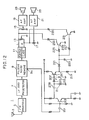
- FIG 3 is a circuit diagram showing one example of the present invention.
- An FM receiver 1 is structured as a so-called car stereo FM receiver.
- An FM electric wave is received by an antenna 3 and is applied to an FM front end 5.
- the FM front end 5 comprises a high frequency amplifier, a local oscillator, a frequency converter, and the like, as is well-known, and the output therefrom is obtained as an intermediate frequency signal.
- the intermediate frequency signal obtained from the FM front end 5 is applied to an IF amplifier/detector 7.
- the IF amplifier/detector 7 may be implemented by an integrated circuit model LA1140 manufactured by Tokyo Sanyo Electric Co., Ltd., for example.
- the structure of the integrated circuit 7 is shown in Figure 4.
- the IF amplifier/detector 7 comprises an IF amplifier 71 of six stages, for example, adapted to receive the intermediate frequency signal from the FM front end 5.
- the output from the IF amplifier 71 is subjected to amplitude limitation by means of a limiter 72 and is applied to a quadrature detector 73 for the purpose of demodulation.
- the output from the detector 73 is applied through an FM mute amplifier 74 to a pulsive noise removing circuit 9 at the subsequent stage.
- the output of the IF amplifier 71 is subjected to level detection by a level detector 75 and the level detected output is applied to a signal intensity indicator 76 and is also applied to the terminal 7a of the circuit 7.
- the terminal 7a corresponds to the fifteenth terminal of the integrated circuit LA1 140.
- the output of the IF amplifier/detector 7 is applied to the pulsive noise removing circuit 9.
- the pulsive noise removing circuit 9 may be implemented by an integrated circuit model LA2101 manufactured by Tokyo Sanyo Electric Co., Ltd., for example. A portion of the integrated circuit 9 (LA21 01) is well-known from Japanese Patent Laying-Open No. 113602/1977 and United States Patent No. 4,066,845 (January 3, 1978). Now referring to Figure 5, the pulsive noise removing circuit 9 will be briefly described.
- the demodulated signal obtained from the IF amplifier/demodulator 7 is applied through a low pass filter 91 and a low pass amplifier 92 to a gate circuit 93.
- the demodulated signal is applied further through an AGC circuit 94 to a high pass filter 95.
- the high pass filter 95 allows a high frequency region of the demodulated signal to pass therethrough and the output therefrom is applied to a noise detector 96 and is also applied to a terminal 9a.
- the noise detector 96 is responsive to the high frequency region signal to detect a noise (a pulsive noise), thereby to trigger a monostable multivibrator 97.
- the output of the monostable multivibrator 97 is applied to the above described gate circuit 93 as a gate control signal.
- the gate circuit 93 is responsive to the output of the monostable multivibrator 97 to gate the modulated output obtained through a low pass amplifier 92 and the output therefrom is applied to an output circuit 98.
- the output circuit 98 serves to provide the output to a stereo demodulating circuit 11 of the subsequent stage and is coupled to a pilot signal holding circuit 99.
- the terminal 9a corresponds to the fourteenth terminal of the integrated circuit LA2101.
- the output from the pulsive noise removing circuit 9, i.e. the output from the output circuit 98 is applied to the stereo demodulating circuit 11.
- the stereo demodulating circuit 11 may be implemented by an integrated circuit LA3370 manufactured by Tokyo Sanyo Electric Co., Ltd., for example.
- the stereo demodulating circuit 11 is responsive to the demodulated output from which a pulsive noise has been removed to provide a left signal and a right signal.
- the output from the pulsive noise removing circuit 9 is applied to the buffer 111 included in the stereo demodulating circuit 11.
- the output from the buffer 111 is applied to a subsequent buffer 112 as a stereo composite signal and is also applied to a subsignal [the difference signal (L%R)] demodulating circuit 114, and to another buffer 113.
- the output of the buffer 112 is applied to a stereo matrix circuit 115 as a sum signal.
- the output of the buffer 113 is applied to a phase locked loop 116.
- the phase locked loop 116 extracts a stereo pilot signal of 19 kHz from the buffer 113 and provides a subcarrier of 38 kHz based on the stereo pilot signal.
- the subcarrier signal from the phase locked loop 116 is applied to the subsignal demodulating circuit 114.
- the stereo matrix 115 is responsive to the two applied signals i.e. the sum signal (L+R) and the difference signal (L-R) and the subcarrier signal to provide a left signal (2L) and a right signal (2R).
- the circuit 11 is provided with a 38 kHz control circuit 117.
- the 38 kHz control circuit 117 controls the subcarrier signal (38 kHz) applied to the stereo matrix 115, thereby to control stereo separation.
- the 38 kHz control circuit 117 is supplied with a voltage signal from the terminal 11 a.
- the terminal 11 a corresponds to the eighth terminal of the integrated circuit LA3370 and the stereo separation is changeable as a function of the magnitude of the voltage being applied to the terminal 11 a.
- the larger the voltage being applied to the terminal 11 a the better the stereo separation, whereas the smaller the voltage the worse the separation.
- the output from the stereo matrix 115 becomes a complete monaural signal.
- the above described left signal and the right signal are balance adjusted by means of a balancing variable resistor 13, so that the left signal is applied through a variable resistor 15 to a low frequency amplifier 19 and the right signal is applied through a variable resistor 17 to a low frequency amplifier 21.
- the low frequency amplifiers 19 and 21 are coupled to drive the corresponding speakers 23 and 25, respectively.
- the terminal 9a of the pulsive noise removing circuit 9, i.e. the output of the high pass filter 95 is applied through a capacitor 201 to the base electrode of a transistor 203 serving as a gain element.
- the transistor 203 receives a bias voltage at the base electrode thereof from a voltage source +B and the collector electrode thereof is coupled through a resistor to the voltage source +B.
- the emitter electrode of the transistor 203 is connected through a switching transistor 205 and a resistor and a capacitor to the ground.
- the base electrode of the switching transistor 205 is connected by a line 205a through a voltage dividing circuit including resistors 7b and 7c to the terminal 7a of the IF amplifier/demodulator 7, i.e. the output of the level detector 75.
- the collector electrode of the transistor 203 is further connected through a double voltage rectifying circuit 207 including capacitors 209 and 215 and diodes 211 and 213 to the base electrode of a transistor 217.
- the collector electrode of the transistor 217 is connected to the voltage source +B and the emitter electrode thereof is connected through a resistor 219 to the ground.
- the emitter electrode of the transistor 217 is connected through a series connection of a diode 221 and a resistor 225 to the base electrode of a switching transistor 229 and further through a series connection of the diode 221 and a resistor 227 to the base electrode of a switching transistor 231.
- the junction of the diode 221 and the resistors 225 and 227 is connected through a capacitor 223 to the ground.
- the capacitor 223 constitutes a charging/discharging circuit.
- the collector electrode of the switching transistor 229 is coupled through a capacitor 233 to the left signal output of the stereo demodulating circuit 11 and the emitter electrode thereof is connected to the ground.
- the collector electrode of the switching transistor 231 is coupled through a capacitor 235 to the right signal output of the stereo demodulating circuit 11 and the emitter electrode thereof is connected to the ground.
- the output of the high pass filter 95 included in the pulsive removing noise 9 is applied to the base electrode of the transistor 203.
- the high pass filter 95 performs an inherent function in the pulsive noise removing circuit 9 but also performs, in the embodiment shown, a function for detecting a higher harmonic level of a distortion component. Accordingly, in case of an FM receiver not including a pulsive noise removing circuit 9, naturally a separate high pass filter may be provided.
- the reason why the high pass filter 95 is used for the purposes of two circuits as in the case of the embodiment shown is that, since the output impedance of the fourteenth terminal of the integrated circuit LA2101 is small, withdrawal of a further signal therefrom exerts no influence upon the characteristic of the circuit 9 and also attains economy.
- FIG. 7 One example of the characteristic of the high pass filter is shown in Figure 7. If a separate, independent high pass filter is provided which has a good characteristic, i.e. an abrupt attenuation, performance of distortion detection to be described would be enhanced accordingly. Meanwhile, a cutoff frequency of the high pass filter 95 is selected to be approximately 100 kHz. Too high a cutoff frequency makes it impossible to detect distortion with sufficient accuracy, while too low a cutoff frequency could cause erroneous detection. Accordingly, the cutoff frequency of the high pass filter needs to be properly selected. Now description will be made of the fact that distortion can be detected by the use of the high pass filter.
- the harmonic level as such is proportional to the distortion ratio D. Accordingly, the output of the high pass filter 95 is associated with the distortion ratio. Therefore, by using the output of the high pass filter 95 as a distortion detected signal, the same can be used in applications other than reduction of a noise and distortion to be described subsequently. For example, although not shown, a distortion amount can be accurately displayed, by providing an amplifier connected to receive the output of the high pass filter 95 as an input thereto, a rectifying circuit connected to receive the output of the amplifier, and a display circuit including a display connected to receive the output of the rectifying circuit.
- a charging/discharging circuit including a capacitor 223 which is one of the features of the present embodiment.
- a charging path of the capacitor 223 is constituted by +B-the collector resistor of transistor 217-transistor 217-diode 221. Accordingly, a resistance component of the circuit associated with the charging time constant is the sum of the internal resistances of the respective elements.
- a reverse resistance (R 221 ) of the diode 221, the resistor 225 (R 225 ) and the base-emitter resistance (R BE ) of the transistor 229, and the resistor 227 (R 227 ) and the base-emitter resistance (R' BE ) of the transistor 231 function in a parallel manner.
- the relationship of the reverse resistance (R 221 ) of the diode 221 to the other resistance components is expressed by the following equation (7).
- the reverse resistance (R 221 ) can thus be neglected for the purpose of calculating the discharging time constant.
- the curve A shows the charging characteristic and the curve B shows the discharging characteristic.
- the curve B shows the discharging characteristic.
- the curve B shows the discharging characteristic.
- the base-emitter resistances R BE and R' BE of the transistors 229 and 231 become larger as the base voltage becomes lower.
- the above described characteristic has no influence upon the switching characteristic, i.e. the recovery time of the transistors 229 and 231 and rather assists a quick response in the case where distortion occurs continuously.
- a composite wave ( Figure 2) of an FM electric wave coming through the antenna 3 is transferred through the FM front end 5 and is demodulated by the IF amplifying/demodulating circuit 7, with distortion contained in the output which is applied to the pulsive noise removing circuit 9.
- the demodulated signal containing distortion applied to the circuit 9 passes through the high pass filter 95 and is withdrawn from the terminal 9a of the circuit 9. The larger the distortion (the distortion rate) contained in the demodulated signal or the higher the demodualted frequency (com), the larger the output level of the high pass filter 95.
- the output of the high pass filter 95 is applied through the capacitor 201 to the base electrode of the transistor 203 and is amplified by the transistor 203, when the switching transistor 205 is in a conductive state, i.e. when the voltage at the terminal 7a of the IF amplifying/demodulating circuit 7 is at a high level.
- the switching operation of the transistor 205 will be described subsequently.
- a noise and distortion component amplified by the transistor 203 is rectified by the double voltage rectifying circuit 207 and the output thereof is applied to the base electrode of the switching transistor 217.
- the switching transistor 217 becomes conductive when the output voltage of the double voltage rectifying circuit 207 exceeds a predetermined value, at which time a current flows from the voltage source +B.
- the current flowing through the transistor 217 is applied to the capacitor 223 (say 47,uF), thereby to rapidly charge the same in accordance with the charging characteristic shown by the curve A in Figure 8.
- the switching transistors 229 and 231 become conductive at the same time. Accordingly, the capacitor 233 is inserted between the left signal output of the output of the stereo demodulating circuit 11 and the ground, while a capacitor 235 is interposed between the right signal output and the ground. Therefore, a high frequency component in the output of the stereo demodulating circuit 11 is reduced. Meanwhile, by properly selecting the values of the capacitors 233 and 235, a high frequency can be fully cut, and furthermore a muting operation can be also performed. Thus a high frequency region of the respective signals being applied to the lower frequency amplifiers 19 and 21 is reduced and an adverse influence exerted upon the auditory sense by a noise and distortion can be mitigated.
- the output voltage of the high pass filter 95 obtained at the terminal 9a of the circuit 9 becomes approximately zero. Since an output of the high pass filter 95 which is approximately zero does not reach the level for rectification by the diodes 211 and 213 of the double voltage rectifying circuit 207 even if the same is amplified by the transistor 203, the switching transistor 217 becomes non-conductive. Accordingly, the transistors 229 and 231 both become non-conductive without a charging current being applied to the capacitor 223. Therefore, the capacitors 233 and 235 are interrupted from the ground and the above described operation for reducing a high frequency component is not performed.
- the above described multi-path distortion fluctuates instantaneously in proportion to the speed of the vehicle. Therefore, a quick response is required for a change from a state in the absence of distortion to a state in the presence of distortion, whereas a delay characteristic is required for a change from a state in the presence of distortion to a state in the absence of distortion.
- the reason is that it is desirable to attain natural recovery. More specifically, in the case of a change from a state in the presence of distortion to a state in the absence of distortion, release of reduction of a higher frequency region in quick response thereto instantaneously increases a signal being applied to the lower frequency amplifiers 19 and 21, which causes a noise offensive to the ears from the standpoint of the auditory sense.
- the embodiment shown has been adapted such that the charging time constant of the charging path and the discharging time constant of the discharging path of the capacitor 223 are selected to be different from each other, whereby the charging/discharging characteristic is set as shown in Figure 8. Therefore, since the embodiment is adapted such that an influence exerted upon the auditory sense by a noise and distortion is mitigated immediately upon occurrence of distortion while natural recovery is attained with a delay time on the occasion of a change to a state in the absence of distortion in the demodulated signal, little auditory sensation of incompatibility is caused because of these additional circuits.
- the impedance of is connected in parallel with the impedance R A and the impedance R B is varied from the value R a to R b .
- the value R a is the impedance in the case where the transistors 229 and 231 are in a fully non-conductive state, i.e. no distortion exists at all. It follows that the impedance R A is shunted by the output impedance of the stereo demodulating circuit 11, the impedances of the variable resistors 15 and 17 and the impedance of the variable resistor 13 and the like, so that the impedance R A becomes several kQ. On the other hand, the above described value R a is several 100k ⁇ .
- the overall impedance Z becomes approximately equal to the impedance R A - More specifically, it follows that the effect of reducing a higher frequency region on the low frequency signals is not significant and as a result the frequency characteristic of the low frequency signals is shown by the curve C in Figure 9.
- the overall impedance Z is expressed by the following equation (8).
- Full conduction of the transistors 229 and 231 means that the above described value R b approximates zero and the equation (8) is expressed by the following equation (8') in an approximate manner.
- the effect of reducing a higher frequency region on the lower frequency signals is expressed by the following equation (9).
- the overall impedance Z is a function of the frequency (f) and accordingly the attenuation amount for an arbitrary frequency is known. The effect of reducing a higher frequency region in such a situation where the switching transistors 229 and 231 are fully conductive is shown by the curve F in Figure 9.
- adjustment of the sensitivity of the circuit with respect to a noise and distortion can be set by properly adjusting the amplification gain by the transistor 203.
- the transistor 205 is provided for the purpose of preventing malfunction.
- Figure 10 is a graph showing the input level of the antenna 3 and the output level of the high pass filter 95 and the output level of the level detector 75.
- the curve G shows the output level of the high pass filter 95
- the curve H shows the output level of the level detector 75.
- the white noise increases as the antenna input becomes small. Since the white noise includes a high frequency level sufficient to pass through the high pass filter 95, assuming the absence of the switching transistor 205 shown in Figure 3, the transistors 229 and 231 become conductive when the antenna input is small or in the absence of the input signal, whereby an operation for reducing the higher frequency region is performed. Accordingly, the embodiment shown is adapted such that the switching transistor 205 becomes conductive whenever the antenna input exceeds a given level, whereby the transistor 203 and thus the transistor 217 are enabled.
- Figure 11 shows the collector current characteristic and gain characteristic of the transistor 203 with respect to the base voltage of the transistor 205.
- the curve I shows the current characteristic
- the curve J shows the gain characteristic.
- the transistor 203 becomes conductive when the base voltage of the transistor 205 becomes approximately 0.4V and becomes in a fully conductive state when the base voltage becomes approximately 0.6V, as shown by the curve J in Figure 11.
- an arbitrary antenna input level is selected based on the output level of the level detector 75 shown by the curve H in Figure 10 and the arbitrary point such as the point K is determined, and the values of the resistors 7 b and 7 c shown in Figure 3 are selected such that the switching transistor 205 may become conductive when the base voltage exceeds the above described point K.
- the transistor 203 and thus the transistor 217 is enabled whenever an arbitrary antenna input level such as the point K is exceeded.
- a circuit associated with the switching transistor 205 is not necessarily required. More specifically, if and when an attempt is made to mitigate even an influence by a noise caused because of a function of an electric wave intensity in accordance with a Rayleigh distribution in a weak electric field area, a circuit associated with the switching transistor 205 is not required. More specifically, in such a case, the switching transistor 205 and the line 205a and the resistors 7 b and 7 c are removed, as shown in Figure 12, so that the emitter electrode of the transistor 203 is connected directly through a resistor or a capacitor to the ground.
- the electric field strength in a weak electric field area is in accordance with a Rayleigh distribution, as described previously. Therefore, an antenna input level of an FM receiver borne on a vehicle travelling in that area fluctuates in accordance with the above described distribution, so that a noise is generated for each fluctuation. Therefore, by operating the circuit for reducing a higher frequency component in the low frequency signals in the level smaller than the antenna input level where a noise is generated because of the Rayleigh distribution, even if a noise is generated based on a fluctuation of the electric field strength because of such Rayleigh distribution, an influence caused by such noise is mitigated, whereby reception can be made with little auditory sensation of incompatibility.
- the bias of the transistor 203 may be set so that the transistor 217 may become conductive at the point K. Then, even if a noise occurs because of the Rayleigh distribution in the antenna input level smaller than the point K, the higher frequency region is reduced by the capacitors 233 and 235 and an influence becomes very little. Furthermore, the lower the antenna input level, the larger is the effect attained. The reason is that the lower the antenna input level the larger the white noise and thus the larger the output of the high pass filter 95.
- the magnitude of a noise because of a variation of the electric field strength based on the Rayleigh distribution and the magnitude of the white noise in the case where the antenna input level becomes small to some extent in the weak electric field area, and the magnitude of the distortion and noise when the composite wave involves a noise and distortion because of a multi-path interference in the middle or strong electric field area is accurately and automatically detected, whereby an operation for reducing a higher frequency region is performed in accordance with the respective magnitudes of the white noise, distortion and the like. Accordingly, in such a case, no sense of incompatibility is given to listeners.
- the magnitude of the white noise, noise or distortion becomes small, the effect of reducing a higher frequency region is naturally released and recovery is made naturally, and as a result a more effective noise and distortion mitigating circuit is provided.
- multi-path distortion can be detected with more accuracy as compared with the conventional detecting circuit.
- the conventional multi-path distortion detector introduces a DC output from a level detector (i.e., a DC output driving a signal level indicator) responsive to an intermediate frequency (IF) signal into a differentiation circuit to extract the variations in carrier amplitude.
- a level detector i.e., a DC output driving a signal level indicator
- IF intermediate frequency
- the variations in carrier amplitude are derived in the form of a DC output as a detection output indicative of multi-path distortion. Consideration is given to the detection accuracy of such a multi-path distortion detector. While the detector output is precisely proportional to multi-path distortion as long as distortion is high, there is incapability of detecting multi- path distortion within a small distortion region.
- the output of the multi-path distortion detector responsive to the input (electric field strength) to the antenna increases due to random noise when the antenna input is below a given level (say, less than about 5 dB).
- a given level say, less than about 5 dB
- the detector will make erroneous decision as if distortion is deteriorated despite fixed multi-path distortion. This is a problem based on the sensitivity of the receivers rather than multi-path distortion.
- the antenna input is above a given level (say, 60dB)
- the DC output of the level detector responsive to the IF signal will become saturated and the carrier amplitude is limited. In this case, the detector senses as if distortion is improved despite fixed multi-path distortion.
- the above described embodiment provides reduction of multi-path distortion and an accurate and effective display of the magnitude of multi-path distortion by leading the output of the FM demodulator to the high pass filter whose output is utilized as the multi-path distortion detecting signal and converted into its corresponding DC signal as the output signal indicative of multi-path distortion.
- multi-path distortion appearing as noise is significantly greater when in stereo receiver mode than when in monaural receiver mode
- multi-path distortion is further suppressed by forcedly altering the operation mode from stereo receiver mode to monoral receiver mode together with reduction of the treble region of the low frequency signal when multi-path distortion appears as noise.
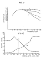
- the following will set forth how much multi-path distortion differs between the FM stereo receiver mode and the monaural receiver mode by reference to the graph of Figure 13.
- distortion factor in monaural receiver mode was no more than 1.5% with 100% modulation, 3 KHz, 10dB of DU ratio (desired-to-undesired signal ratio), 10 ⁇ sec of delay time and 60° of phase difference.
- the line L represents characteristics in stereo receiver mode (only left signals) and the line M those in manoural receiver mode.
- a further reduction in multi-path distortion can thus be achieved by provision of means for forcedly placing a receiver into a monaural receiver mode upon the development of multi-path distortion.
- means for forcedly placing a receiver into a monaural receiver mode upon the development of multi-path distortion.
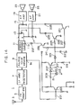
- the receiver is forcedly brought into monaural receiver mode with OdB of separation by grounding a left and right signal separation adjusting terminal 11 a of integrated circuit LA3370 constituting the FM stereo demodulator 11 (that is, it corresponds to terminal 8 of LA3370).
- the remaining circuit arrangement is identical with that in Figure 3.
- the switching transistors 229 and 231 become non-conductive as shown in Figure 3 to inhibit attenuation of the treble region of the output of the FM stereo demodulator 11. Since the switching transistor 239 is in non-conductive state under these circumstances, the FM stereo demodulator 11 persists in the normal stereo receiver mode rather than in monaural receiver mode.
- the distortion reduction circuit for use in FM receivers according to the embodiment of Figure 14 ensures a further reduction in distortion by provision of the addition means for the receiver forcedly altering the receiver from stereo receiver mode into manoural receiver mode upon the development of multi-path distortion.
- Figures 15 and 16 are schematic diagrams of further embodiments of the present invention, respectively.
- the FM receiver 1 is combined with a cassette type tape recorder, not shown.
- the Figure 15 embodiment corresponds to the previously described Figure 3 embodiment and the Figure 16 embodiment corresponds to the previously described Figure '12 embodiment.
- circuits of Figures 15 and 16 further include a switch 303 and a resistor 305 serially connected between the power supply +B and the base of the switching transistor 217.
- the switch 303 is adapted to be operative only when the equipment is switched from tape recorder mode to radio mode and in other words only when a tape/radio selection and ejection button is depressed.
- the tape/radio selection and ejection button is actuated to shift the operation mode from tape recorder mode to radio mode when the switch 301 is rendered ON state.
- the switch 303 is turned on and the base of the transistor 217 is supplied with a bias voltage from the power supply +B via the resistor 305. Therefore, the transistor 217 is turned on unconditionally regardless of whether multi-path distortion is present, thus permitting quick charging of the capacitor 223 according to the charging characteristic as depicted by the line A in Figure 8 and eventually turning the transistors 229 and 231 on.
- the capacitor 223 is gradually discharged according to the discharging characteristic as depicted by the line B in Figure 8.
- the transistors 229 and 231 are thus held in on state within 2-3 seconds of tape-to-radio mode transition. The phenomenon is of great importance in reducing noise occurring upon the tape-to-radio mode selection.
Landscapes
- Engineering & Computer Science (AREA)
- Computer Networks & Wireless Communication (AREA)
- Signal Processing (AREA)
- Noise Elimination (AREA)
- Stereo-Broadcasting Methods (AREA)
Claims (11)
Applications Claiming Priority (8)
| Application Number | Priority Date | Filing Date | Title |
|---|---|---|---|
| JP164297/79 | 1979-12-17 | ||
| JP16429779A JPS5686537A (en) | 1979-12-17 | 1979-12-17 | Noise and distortion reduction circuit of fm receiver |
| JP16702779A JPS5689142A (en) | 1979-12-21 | 1979-12-21 | Multipath distortion detecting circuit of fm receiver |
| JP167027/79 | 1979-12-21 | ||
| JP182738/79 | 1979-12-27 | ||
| JP18273879 | 1979-12-27 | ||
| JP146691/80 | 1980-10-14 | ||
| JP14669180U JPS5769339U (fr) | 1980-10-14 | 1980-10-14 |
Publications (2)
| Publication Number | Publication Date |
|---|---|
| EP0030874A1 EP0030874A1 (fr) | 1981-06-24 |
| EP0030874B1 true EP0030874B1 (fr) | 1984-04-25 |
Family
ID=27472731
Family Applications (1)
| Application Number | Title | Priority Date | Filing Date |
|---|---|---|---|
| EP80304577A Expired EP0030874B1 (fr) | 1979-12-17 | 1980-12-17 | Circuit de réduction des distorsions pour un récepteur à modulation de fréquence |
Country Status (3)
| Country | Link |
|---|---|
| US (1) | US4416024A (fr) |
| EP (1) | EP0030874B1 (fr) |
| DE (1) | DE3067653D1 (fr) |
Families Citing this family (21)
| Publication number | Priority date | Publication date | Assignee | Title |
|---|---|---|---|---|
| NL8203384A (nl) * | 1982-08-31 | 1984-03-16 | Philips Nv | Fm-stereo-ontvanger. |
| JPS60165834A (ja) * | 1984-02-09 | 1985-08-29 | Clarion Co Ltd | 自動周波数制御回路 |
| JPS61202537A (ja) * | 1985-03-06 | 1986-09-08 | Clarion Co Ltd | Fmステレオ受信機におけるステレオ雑音低減回路 |
| JPH0669150B2 (ja) * | 1985-05-16 | 1994-08-31 | クラリオン株式会社 | Fm受信機 |
| US5036543A (en) * | 1989-06-30 | 1991-07-30 | Pioneer Electronic Corporation | Noise suppression apparatus for FM receiver |
| JPH03259622A (ja) * | 1990-03-09 | 1991-11-19 | Pioneer Electron Corp | ノイズ低減回路 |
| US5375259A (en) * | 1992-02-20 | 1994-12-20 | Lee; Denny L. Y. | Analog signal noise reduction process and apparatus |
| US5406588A (en) * | 1993-05-28 | 1995-04-11 | Motorola, Inc. | Method and apparatus for mitigating distortion effects in the determination of signal usability |
| US5583891A (en) * | 1994-10-31 | 1996-12-10 | Motorola, Inc. | Noise attenuation circuit for amplitude modulated radio and method therefor |
| EP0797872A4 (fr) * | 1994-11-29 | 1999-03-31 | Gallagher Group Ltd | Procede de commande electronique |
| JPH08265047A (ja) * | 1995-01-24 | 1996-10-11 | Matsushita Electric Ind Co Ltd | 周波数変換回路 |
| DE19540183A1 (de) | 1995-10-27 | 1997-04-30 | Bosch Gmbh Robert | Stereorundfunkempfänger |
| DE19542737A1 (de) * | 1995-11-16 | 1997-05-22 | Bayerische Motoren Werke Ag | Schaltanordnung für mobile Rundfunkempfänger |
| US6944301B1 (en) | 1999-03-10 | 2005-09-13 | Cirrus Logic, Inc. | Method and apparatus for discriminating multipath and pulse noise distortions in radio receivers |
| EP1069693B1 (fr) * | 1999-07-15 | 2004-10-13 | Mitsubishi Denki Kabushiki Kaisha | Dispositif de réduction de bruit |
| US20030022681A1 (en) * | 2001-07-24 | 2003-01-30 | Ruppel Christopher D. | Adaptive dynamic technique for multi-path signal processing |
| US7177608B2 (en) * | 2002-03-11 | 2007-02-13 | Catch A Wave Technologies | Personal spectrum recorder |
| US7359686B2 (en) * | 2005-02-16 | 2008-04-15 | Microtune (Texas), L.P. | Radio-frequency amplifier system |
| JP4916974B2 (ja) * | 2007-08-03 | 2012-04-18 | オンセミコンダクター・トレーディング・リミテッド | Fmチューナ |
| DE102012201372A1 (de) * | 2012-01-31 | 2013-08-01 | Sennheiser Electronic Gmbh & Co. Kg | Stationärer, analoger FM-Empfänger zum Empfangen von analogen, drahtlos übertragenen FM-Audiosignalen von mindestens einer mobilen Einheit und Verfahren zum Empfangen eines analogen, frequenzmodulierten Audiosignals von einem mobilen analogen FM-Sender |
| DE112016003942T5 (de) * | 2015-08-31 | 2018-05-24 | Asahi Kasei Microdevices Corporation | Demodulator |
Citations (1)
| Publication number | Priority date | Publication date | Assignee | Title |
|---|---|---|---|---|
| US3539729A (en) * | 1967-06-12 | 1970-11-10 | Scott Inc H H | Apparatus for reducing interference in the transmission of electric signals |
Family Cites Families (10)
| Publication number | Priority date | Publication date | Assignee | Title |
|---|---|---|---|---|
| US2363649A (en) * | 1941-10-25 | 1944-11-28 | Rca Corp | Frequency modulation receiver |
| US3569633A (en) * | 1967-12-21 | 1971-03-09 | Heath Co | Fm stereo receiver having automatic threshold switching circuitry |
| NL164435C (nl) * | 1971-06-24 | 1980-12-15 | Philips Nv | Ontvanginrichting. |
| DE2512412C3 (de) * | 1975-03-21 | 1979-02-01 | Blaupunkt-Werke Gmbh, 3200 Hildesheim | Schaltungsanordnung zum Unterdrücken von Störungen in einem FM-Rundfunkempfänger |
| US3979679A (en) * | 1975-06-30 | 1976-09-07 | California Microwave, Inc. | FM demodulator having squelch circuit using bucket brigade delay line |
| IT1052399B (it) | 1975-11-25 | 1981-06-20 | Autovox Spa | Circuito elettronico per la soppressione dei disturbi nei radioricevitori |
| JPS5816653B2 (ja) * | 1976-03-19 | 1983-04-01 | 三洋電機株式会社 | Fm受信機のパルス性雑音除去装置 |
| US4210094A (en) * | 1976-04-30 | 1980-07-01 | Olympus Optical Co., Ltd. | Radio tuner for coupling with cassette tape recorder |
| US4063039A (en) * | 1976-06-16 | 1977-12-13 | General Motors Corporation | Stereo noise reduction circuit |
| US4278901A (en) * | 1978-06-09 | 1981-07-14 | Sanyo Electric Co., Ltd. | Pulsive component detecting apparatus |
-
1980
- 1980-11-26 US US06/210,378 patent/US4416024A/en not_active Expired - Lifetime
- 1980-12-17 DE DE8080304577T patent/DE3067653D1/de not_active Expired
- 1980-12-17 EP EP80304577A patent/EP0030874B1/fr not_active Expired
Patent Citations (1)
| Publication number | Priority date | Publication date | Assignee | Title |
|---|---|---|---|---|
| US3539729A (en) * | 1967-06-12 | 1970-11-10 | Scott Inc H H | Apparatus for reducing interference in the transmission of electric signals |
Also Published As
| Publication number | Publication date |
|---|---|
| DE3067653D1 (en) | 1984-05-30 |
| EP0030874A1 (fr) | 1981-06-24 |
| US4416024A (en) | 1983-11-15 |
Similar Documents
| Publication | Publication Date | Title |
|---|---|---|
| EP0030874B1 (fr) | Circuit de réduction des distorsions pour un récepteur à modulation de fréquence | |
| US4380824A (en) | Receiving reproducing system | |
| US4390749A (en) | Noise control system for FM radio | |
| US4379207A (en) | Automatic noise eliminating device for an FM receiver | |
| US5432854A (en) | Stereo FM receiver, noise control circuit therefor | |
| US4356568A (en) | Receptive condition automatic selection device for FM receiver | |
| US4029906A (en) | Automatic noise reduction system of FM stereo receiver | |
| US3999132A (en) | Stereo inhibit circuit | |
| US4399325A (en) | Demodulating circuit for controlling stereo separation | |
| US4087641A (en) | Noise limiting circuit for FM stereo receiver | |
| US5068896A (en) | Audible noise reducing | |
| CA1129011A (fr) | Attenuateur audio de recepteur radio | |
| JP2601764Y2 (ja) | Fmチューナ | |
| US4809328A (en) | FM/FMX stereophonic receiver | |
| EP0013149A1 (fr) | Démodulateur pour signal radiophonique stéréo modulé en fréquence | |
| JPH0354443Y2 (fr) | ||
| EP0047522B1 (fr) | Circuit pour identification d'un signal stéréophonique | |
| JPH0752851B2 (ja) | Fm受信装置 | |
| JPS5931077Y2 (ja) | Fmステレオ受信機 | |
| US5136649A (en) | Fm stereophonic receiver | |
| JPS6228896B2 (fr) | ||
| KR850000841B1 (ko) | Am 스테레오 수신기 | |
| JP3221280B2 (ja) | マルチパスノイズ低減装置 | |
| JPH01255331A (ja) | Fmステレオ受信機 | |
| US5202925A (en) | Fm stereophonic receiver |
Legal Events
| Date | Code | Title | Description |
|---|---|---|---|
| PUAI | Public reference made under article 153(3) epc to a published international application that has entered the european phase |
Free format text: ORIGINAL CODE: 0009012 |
|
| AK | Designated contracting states |
Designated state(s): DE FR GB |
|
| 17P | Request for examination filed |
Effective date: 19811223 |
|
| GRAA | (expected) grant |
Free format text: ORIGINAL CODE: 0009210 |
|
| AK | Designated contracting states |
Designated state(s): DE FR GB |
|
| REF | Corresponds to: |
Ref document number: 3067653 Country of ref document: DE Date of ref document: 19840530 |
|
| ET | Fr: translation filed | ||
| PLBE | No opposition filed within time limit |
Free format text: ORIGINAL CODE: 0009261 |
|
| STAA | Information on the status of an ep patent application or granted ep patent |
Free format text: STATUS: NO OPPOSITION FILED WITHIN TIME LIMIT |
|
| 26N | No opposition filed | ||
| PGFP | Annual fee paid to national office [announced via postgrant information from national office to epo] |
Ref country code: FR Payment date: 19991208 Year of fee payment: 20 |
|
| PGFP | Annual fee paid to national office [announced via postgrant information from national office to epo] |
Ref country code: GB Payment date: 19991215 Year of fee payment: 20 |
|
| PGFP | Annual fee paid to national office [announced via postgrant information from national office to epo] |
Ref country code: DE Payment date: 19991220 Year of fee payment: 20 |
|
| PG25 | Lapsed in a contracting state [announced via postgrant information from national office to epo] |
Ref country code: GB Free format text: LAPSE BECAUSE OF EXPIRATION OF PROTECTION Effective date: 20001216 |
|
| REG | Reference to a national code |
Ref country code: GB Ref legal event code: PE20 Effective date: 20001216 |