EP0031183A2 - Mehrrechner-Datenverarbeitungssystem - Google Patents
Mehrrechner-Datenverarbeitungssystem Download PDFInfo
- Publication number
- EP0031183A2 EP0031183A2 EP80201185A EP80201185A EP0031183A2 EP 0031183 A2 EP0031183 A2 EP 0031183A2 EP 80201185 A EP80201185 A EP 80201185A EP 80201185 A EP80201185 A EP 80201185A EP 0031183 A2 EP0031183 A2 EP 0031183A2
- Authority
- EP
- European Patent Office
- Prior art keywords
- error
- code
- word
- data
- peripheral equipment
- Prior art date
- Legal status (The legal status is an assumption and is not a legal conclusion. Google has not performed a legal analysis and makes no representation as to the accuracy of the status listed.)
- Granted
Links
Images


Classifications
-
- H—ELECTRICITY
- H03—ELECTRONIC CIRCUITRY
- H03M—CODING; DECODING; CODE CONVERSION IN GENERAL
- H03M13/00—Coding, decoding or code conversion, for error detection or error correction; Coding theory basic assumptions; Coding bounds; Error probability evaluation methods; Channel models; Simulation or testing of codes
- H03M13/03—Error detection or forward error correction by redundancy in data representation, i.e. code words containing more digits than the source words
- H03M13/05—Error detection or forward error correction by redundancy in data representation, i.e. code words containing more digits than the source words using block codes, i.e. a predetermined number of check bits joined to a predetermined number of information bits
- H03M13/13—Linear codes
-
- G—PHYSICS
- G06—COMPUTING OR CALCULATING; COUNTING
- G06F—ELECTRIC DIGITAL DATA PROCESSING
- G06F11/00—Error detection; Error correction; Monitoring
- G06F11/07—Responding to the occurrence of a fault, e.g. fault tolerance
- G06F11/08—Error detection or correction by redundancy in data representation, e.g. by using checking codes
- G06F11/10—Adding special bits or symbols to the coded information, e.g. parity check, casting out 9's or 11's
Definitions
- the invention relates to a multi-processor com- . puter system containing a number n (n 7 2) of processor elements operating in parallel, each of which have a first data input and a first data output, which computer system further comprises a memory with second data inputs to receive information appearing on the data outputs mentioned above and to store this information temporarily and also with second data outputs to present information to the first data inputs mentioned, whereby a closed path can be formed, containing an information-reconstruction device to receive, reconstruct and re-inject all the information circulating in the closed path on the basis of an error-correcting code. All information processing is subject to errors.
- the second data inputs and the second data outputs may in fact be physically the same pair of terminals which are then bi-directional. This may also be the case for the first data input and the first data output.
- a system as described above, with n 3, is suitable for the comparison each time of three parallel bits present in the closed path and for the reconstruction of the correct information value on the basis of a majority decision.
- the information-reconstruction device can be single but then no correction is possible for errors that arise in the information-recon- st ruction device itself. If the reconstruction device is also present in three-fold, extra connections are neces- sa ry so that each time all information is fed to each of the information-reconstruction device.
- the act u al quantity of signals is n symbols of b bits.
- the code is said to be systematic at bit level if each of the b x k information bits can be reconstructed from precise- l y one of the b x n code bits ; b . (n-k) bits are thus re- du ndant.
- the code is said to be systematic at symbol le- vel if each of the k information symbols, which together contain the whole information content, can be reconstruct- ed from precisely one code symbol ; (n-k) symbols are then redundant.
- Non-systematic codes are also possible but the coding/decoding devices are then often more complicated.
- a “distance” quantity may now be defined, which is a property of the code. According to Hamming, the distance is the minimum value of the smallest difference, in number of bits, between any arbitrary pair of code-words.
- the code is now defined as having a "distance" of D over the symbols ; D is the minimum value of the smallest difference in number of symbols between any arbitrary pair of code-words. In a multiple bit symbol the value of this difference can be different (provided it is not equal to zero).
- D 6 it is possible either to make 3 errors detectable, 2 of which can be corrected, or 4 errors detectable of which one can be corrected, or 5 errors detectable of which none can be corrected.
- the omission or restriction of the correction facility can be advantageous where the correction operation causes a delay or where, in certain cases, it is desired to have the greatest possible certainty that no erroneous code word is passed through as correct.
- the invention is based on the realization that it is possible to reduce the redundancy in certain parts of a system by an extra investment in other parts of the system and, in particular, to process a larger quantity of information in these parts. It is thereby an object of the invention to realize a cheaper computer system by a reduced requirement in memory capacity, against which only a limited increase in processor capacity is needed.
- a multi-processor computer system comprising a plurality of n, where n ⁇ 4 error-isolation areas, each isolation area including a parallel operating processor having an input and an output which is coupled to a memory section for storing temporarily the information derived from the processor output, an output of the memory section is coupled to the input of the processor thereby to form a retro coupled path for the information, an information reconstruction section in each retro coupled path, each information-reconstruction section having n inputs for receiving all the information circulating in all the retrocoupled paths of the n error-isolation areas, and an encoder coupled between the processor output and the memory section, the encoder on the basis of a data-word generated by the processor and constructed of k symbols, each of b bits forming a code-symbol of b bits for storage in the corresponding memory section , as part of a code-word consisting of n code-symbols belonging to a set of code-words with a code-distance, defined over
- the information-reconstruction device becomes more complex than in the prior art, but the reduced memory capacity makes the system cheaper.
- the saving in costs is obtained because a code-symbol shorter than the corresponding data word is formed in each encoder. In each error isolation area (see below), therefore, a data reduction takes place in two stages : first in the information reconstruction section from code-word to data word and then in the encoder from data-word to code-symbol.
- the encoders mentioned are suitable for transmitting the (n-2) data-symbols mentioned without further coding as elements in the code-symbols mentioned.
- the data-symbols are preferably taken over directly as code-symbols.
- Each error-isolation area may have a register for one code-word at the input to the information reconstruction sector.
- the operation of the elements in the various error-isolation areas is mutually synchronous. Some inequality of phase is however permissible.
- the purpose of the input register is to ensure that the input information (the code-word may or may not be erroneous) no longer changes at the moment that the information reconstruction sector begins with the reconstruction of the data-word. This is necessary because for example otherwise a combinatorial network therefore would receive a changing signal and that would give rise to an indeterminate output signal.
- At least one of the information reconstruction sections may be provided with a signal output for indicating the detection of a correctable or non-correctable error. If the error is such that reconstruction is impossible, the error detection signal can be used to start a "repeat" operation. If reconstruction is possible, the detection signal can be used to up-date a file giving the degree of unreliability of the various error-isolation areas. In the event of an error that cannot be corrected, the most unreliable isolation area may be ignored.
- the processor element for the connection of a peripheral apparatus, in a first error-isolation area, is provided with at least one outgoing control line and with an output line for a data word for the peripheral apparatus concerned, and that further in all error-isolation areas the respective processor element is provided with at least one incoming control line and an incoming line for a data word from that peripheral equipment and that, further, all the incoming lines mentioned are provided with switches that can be activated in a blocking way by an output signal from the corresponding processor element.
- Peripheral equipment can be of various types : input/output devices such as keyboards, displays or printers, background memories such as magnetic disk memories with corresponding control circuits and finally, it may be a second computer system, for example, a subordinate or front-end processor.
- the last-mentioned system represents a simple and cheap solution.
- the operation of the peripheral equipment is not then included in the pro- . tection given by the redundancy mentioned earlier.
- the control lines concerned will be a request line in the outgoing direction and an acknowledge line in the incoming direction.
- the peripheral equipment may be embodied in a call-organization (polling).
- a sensor + A/D converter may be concerned which, when called, transmits the value of some measured analog quantity in digital form. The ingoing control line for each error-isolation area is then not required.
- first means to receive the code-symbols from all error-isolation areas formed by the corresponding encoders of and on the basis thereof to reconstruct the corresponding data-word
- the processor element is provided with at least one outgoing control line for that peripheral equipment and a second encoder and that the peripheral equipment mentioned is provided with second means to form from the decoded control signals from each error isolation area a control word on the basis of the same symbol-correcting code as that used for the code-word
- the processing element concerned is provided with at least one incoming control line and with an incoming line for a data-word from that peripheral equipment and that further all the incoming lines mentioned are provided with switches that can be activated in a blocking manner by an output signal from the corresponding processor element.
- this is provided with first means to receive from all error-isolation areas the code-symbols formed by the corresponding encoder and on the basis of that received to reconstruct the corresponding data-word, and further with third means to form a code-word from a data-word that has been formed by means of encoding as in the error-isolation areas, that further in each error-isolation area the processor element is provided with at least one outgoing control line for that peripheral equipment and a second encoder and that the peripheral equipment mentioned is provided with second means to form a control word from the control signals so encoded in each error-isolation area, on the basis of the same symbol-correcting code as used for the code-word, that further in each error-isolation area the processor element concerned is provided with at least one incoming control line from that peripheral equipment and the information reconstruction section is so connected by way of a switching device to be driven in a blocking way by an output signal from the processor element in question, that it can receive a whole code-word generated in the peripheral
- each second error-isolation area is provided with first means to receive the code-symbols formed by the corresponding encoder from all first error-isolation areas and on the basis of that received to reconstruct each corresponding data-word and further with fourth means to form a code-symbol from a data-word produced by way of encoding each time as in a corresponding first error-isolation area, that, further, the processor element in each first error-isolation area is provided with at least one outgoing control line for the peripheral equipment and a second encoder and that the peripheral equipment mentioned is provided in each second error-isolation area with second means to form a control word from the coded control signals from each first error-isolation area, on the basis of a symbol-correcting code, that further all first error-isolating areas are provided with fifth means to receive from all second error-isolation areas at least one control signal and therefrom to form a corresponding combined control signal and to
- peripheral equipment mentioned has n second error-isolation areas. This makes for a balanced and symmetrical structure.
- a symbol is a bit group consisting of a fixed number of bits, for example M.
- the symbol can thus have 2 M different values and can be regarded as an element of a Galois field, denoted in this case by GF (2 M ).
- GF Galois field
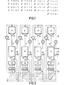
- bit 1 shows the sixteen elements of the Galois field GF(2 4 ) once as a power series and once as a bit group.
- the bit groups can be formed by using the so- called primitive and irreducible polynominal x 4 + x + 1.
- the quantities a°, a 1 , a 2 , a3 are in this example linearly independent of each other.
- the value of M is, in principle, arbitrary.
- the element 0 (bit-wise 0000) and a o (0001) are for brevity to be written from now on as 0 and 1 however it should be remembered that they represent symbols).
- the computer system works on the basis of data-words of 8-bits. These words can be regarded as being built up of two data-symbols, each of four bits.
- each code symbol c i is an element of GF(2 ) and each c ij is an element of GF(2). In GF(2) the elements can only have the values 0 and 1.
- Each row consists of as many symbols as the code-word possesses code-symbols.
- a code-word can be corrected by this code, if it contains at most one erroneous code-symbol (erroneous in arbitrary fashion).
- the error locator which indicates which code-symbol is erroneous, can be derived easily and unambiguously : if both symbols of the vector s have the value o there is no error. If only the first symbol of the vector s has the value o, only the second code symbol is erroneous. If only the second symbol of the vector s has the value o, then only the first code symbol is erroneous. If both symbols of the vector s have the same non-zero value, the third code symbol is erroneous. If neither symbol of the vector s is equal to zero, it may be that only the fourth symbol is erroneous. In that case a check is necessary to see if these two symbols are related as e : (a 1 .e). In the case described this check is simple :
- the columns of the left-hand matrix form the binary representations of a 4 , a3, a 2 and a 1 , respectively. If one of the five cases described occurs, the "error value" (as opposed to the "error locator” mentioned above) is given by the first symbol of the vector s , unless this symbol has the value o (which implies that the second code symbol is erroneous).
- the redundancy bits are generated by the generator matrix [G] , which is related to the parity check matrix [H] in known way by:
- the minimum number of bits per symbol is 2. If there were 1 bit per symbol a partial code-word occurs of four bits with two redundancy bits ; the number of redundancy bits is then too small for a correct correction.
- the sixteen-bit code-word is now split into two eight-bit partial code-words : the first partial code-word contains the first, second, fifth, sixth, nineth, tenth, thirteenth and fourteenth bits : the second partial code-word contains the eight other bits. We can then write :
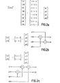
- Fig. 2b shows the formation of the first two-bit code symbol and fig. 2c the formation of the second two-bit code-symbol, both in matrix form and showing the realization by means of logical EXCLUSIVE-OR gates or modulo-2 adders. The latter are represented by a circle containing a cross. Synchronization and other control signals are not indicated in figures 2b and 2c, for simplicity. The generation of the other two code-symbols in this systematic code are simply given by :
- the data symbols involved are thus unchanged as parts of the code-word.
- the sequence of the code-symbols within the code-word can of course be different.
- a decoder to reconstruct the data word from the corresponding code-word will be discussed later.
- Fig. 3 shows a simple version of a computer system in accordance with the invention, on the basis of the information being organized in bit groups (bytes) of eight bits. These are assumed to possess no redundancy ; if this information were processed in parallel in a uni-processor system, all data routes would have a width of 8 bits and the local memory of the processor would also have a word length of 8 bits.
- the arrangement of fig. 3 is a four-fold system in which each byte of information is represented in each processor by eight information bits and in the local memory sector of each processor (processor element) by four code bits. If the memory is expensive.compared to the processors, this implies that this system is twice as expensive as the uni-processor system.
- peripheral equipment that is to say, without implementation of lines 90, 92, 94, 96. Furthermore, the extreme right-hand side of the figure comprising the elements 12, 28, 46 and 54 will be discussed.
- FIG. 4 shows a suitable microprocessor for use as a processor element 12 in Fig. 3.
- This element is described in the book "Signetics 2650 microprocessor” published by the manufacturer, Signetics Corporation, 811 East Arques ' Ave., Sunnyvale, Cal. USA 1975, notably in Fig.1 thereof.
- the numbers within circles represent the 8-bit data paths and the 13/15 bit address paths.
- the connections marked "1" or "x" are part of the control bus.
- Line 200 is a bi-directional data bus with attached register 202.
- the incoming line 204 is connected to the 8-bit instruction register 206, the 8-bit hold register 208, an 8-bit input to the address adder 210 (this works over a width of 13 bits) and to a data connection of the arithmetic and logic unit (ALU) 240 (working over a width of 8 bits).
- An interrupt-request signal from outside can appear on line 214.
- Line 216 is reserved for an interrupt-acknowledge signal.
- the microprocessor concerned has a connection (not shown here) for the reception of a pause signal which causes it to stop at the end of the current instruction. This pause signal can terminate the processing of data for an indefinite time; it is used to realize direct memory access (DMA).
- DMA direct memory access
- the interrupt logic is contained in block 212. This block can also send a signal to the interrupt and control logic in block 218.
- Lines 220 are the input/output control lines. The signals on these lines cooperate with the logic block 222 and also block 218.
- Line 224 is an external clock-pulse line; these clock-pulses are processed in the time-generating logic 226 to secondary clock pulses for block 218. For simplicity the outgoing control lines from block 218 to the further elements of the circuit are not shown.
- a second thirteen-bit wide input of the address adder 210 is connected to the address bus 228, the external connections of which are only suitable for the transmission of signals.
- Element 230 is the operand address register
- element 232 is the instruction address register
- element 234 is the address output control element
- element 236 is the sub-routine return address stack
- element 238 the stack pointer.
- the internal control is done by signals from block 218 and by the contents of the program status word in element 242.
- a register stack which contains the zero register 246 and 2 x 3 registers in the further stack element 248.
- Element 250 is a multiplexer.
- Block 252 contains logic for the condition code and for possible branches. For the functions realizable by this microprocessor and for other technical details reference should be made to the manufacturers book cited above.
- an 8-bit data word appears on line 62 (corresponding to line 200 in Fig. 4).
- This is processed in processor element 12, the nature of the operations depending on the purpose for which the computer system is used. It can thus involve the up-dating of a data file or the execution of some complex scientific calculation, or, for example, the processing of parameters to generate one or more control quantities in an industrial control system.
- the microprocessor 12 produces an output data-word on line 78 (line 299 in Fig. 4) and an address word on line 70 (line 228 in fig. 4) to address the local memory 28 by means of the addressing device 27 (containing, for example, a decoder).
- a four-bit code symbol is formed from the 8-bit data-word received, and is presented to the memory 28 where it is stored.
- the information read-out from the memory 28 appears as a code symbol on line 81 and is regenerated in the read-out amplifier(s) 36 which possess an adequate margin of fan-out. In this way the code symbol is presented on line 88. This can also be done without intermediate storage in memory 28.
- the lines 78 and 62 are thus interconnected.
- the information reconstruction sector 54 acts, with respect to this microprocessor, as the only information source and the encoder 20 acts as the only information destination.
- the system described above is present in four-fold (processor elements 12, 14, 16, 18 and, memory sections 28, 30, 32, 34 with the corresponding circuits) and except for the encoders 20, 22, 24, 26 (see later), all these systems are identical. Moreover, the processor elements 12, 14, 16, 18 all operate according to the same program and they hence carry out the same operations together.
- the instructions of this program can also be encoded to code-words which are stored in the memory sections 28, 30, 32, 34. Another possibility is that the instructions are stored separately in each error-isolation area. The synchronization of the operation of the four error-isolation areas is not shown. The various means of synchronization are described in an article by D. Davies et al. "Synchronization and matching in redundant systems", IEEE Trans. Comp. Vol. C.27 (June 1978), pp. 531 - 539.
- encoder 20 contains a circuit to allow theb irst two bits of the data-word to pass through for the first code-word and a circuit as in Fig. 2b to form a redundant code-symbol for the second code-word.
- Encoder 22 contains a circuit to allow the second two bits of the data-word to pass through for the first code-word and a circuit as in Fig. 2c for the second code-word.
- Encoder 24 contains a circuit to allow the third two bits of the data-word to pass through for the second code-word and a circuit as in Fig. 2b for the first code-word.
- Encoder 26 contains a circuit to allow the fourth two bits of the data-word to pass through for, the second code-word and a circuit as in Fig. 2c for the first code-word. In fact, in this way each encoder only needs to receive six bits of the data-word.
- each processor element has its own information reconstruction section, blocks 54, 56, 58, 60, with their input registers 46, 48, 50, 52. These registers each receive all information (16 bits) read out together from the respective memories via the respective connections 82, 84, 86, 88, for the data-word to be reconstructed in the information reconstructors.
- Each code-word may possess one erroneous code-symbol of two bits, i.e. there are 4 x 3 possibilities for a correctly corrigible word because the error (the error symbol) may have three values.
- the remaining 48 possibilities involve a double or multiple error.
- the ROM may deliver an error indication if one of the memory locations concerned is addressed.
- the error-locator in the event of an error occurring in one of the error-isolation areas it is also possible to produce the error-locator. In this case that would imply that an 8-bit (half) code-word would be received.
- the corrected errors can be collected in a histogram that shows how often a given error-isolation areas has given an error. Under the control of the signal from an incorrigible error, the following further attempts at correction are possible, e.g.
- the indication "double error” can be generated once or twice per data-word. These indications ' are combined by an OR gate in the known manner. This is not shown in the figure.
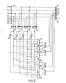
- This circuit is present, 1 x or 2 x, for each of the building blocks 54, 56, 58, 60 shown in Figure 3.
- There is an 8-bit input line 130 which receives two bits from each of the partial memories. The upper four lines carry the information bits, the lower four lines the redundancy bits.
- the redundancy bits are regenerated as in Figs. 2b and 2c and compared with the current redundancy bits on the lower four input lines. If such a gate gives off a logical "O", this means that no error has occurred; these gates can themselves be known circuits according to U.S. Patent Specification 3 838 393.
- the error-indication bits formed in this way are fed via the inverters 140, 142, 144, 146 to the six AND gates 148, 100, 102, 104, 106, 108 and from there to the four NAND gates 110, 112, 114, 116. In this way, all the matrix multiplications discussed here above are formed in order to generate the corrector-symbol. This is added bit-wise (modulo 2) in the elements 118, 120, 122, 124, to the data information to correct possible errors.
- the outputs of the elements 118-124 are connected to a clocked data register from which the information is made available to be processed in the microprocessor, for example, the register 202 in Fig. 4.
- the elements 12, 20, 28, 36, 46, 54 formed parts of the same error-isolation area.
- the circuit of Fig. 3 contains four such areas each with similar circuits. Within each such area the errors occurring may be correlated. The errors occurring in different isolation areas are assumed to be independent of each other, as is the case in practice for many categories of error. The probability of errors in more than one area is then equal to the product of the probabilities in the separate areas ; in general such a product has a very small value.
- the various areas are joined together by the lines 82, 84, 86, 88. The probability of errors occurring during the signal transmission in these lines can be made small by taking suitable measures (e.g. the amplifier 36).
- the errors within a single isolation area may thus have any value, even in the sense that the isolation area is completely inoperative. If the elements 12, 20, 28, 36, 46, 54 are all mounted on a single printed circuit board or in a single I.C. module, the whole board/module, may be then removed without the occurrence of a malfunction. This means that a service technician can remove the faulty elements while the system is working, often without disturbing the operation of the system.
- the data routes shown in Fig. 3 have the following bit widths :
- the memory sections 28, 30, 32, 34 are conventional building blocks and will not be discussed further.
- Fig. 3 contains certain additions for the connection of peripheral equipment, for example an input/ output device for data information. It is assumed that this device produces error-free information ; this arrives, for example as 8-bit words, on line 96.
- This line can be connected via the interrupt switches 61, 63, 65, 67 to the information input lines 62, 64, 66, 68 of the processor elements 12, 14, 16, 18 respectively.
- there is a control line 94 from the peripheral equipment which is connected via the interrupt switches 99, 101, 103, 105 to the input/output control connections of the processors 12, 14, 16, 18, respectively.
- the information can be fed to the peripheral equipment via the 8-bit line 90, which is a branch of line 78.
- This line 78 at least, must be an 8-bit line and thus transmit more information than the minimum necessary for the encoder 20.
- a control signal is fed to the peripheral equipment via line 92 which comes from processor element 12.
- the peripheral equipment is not connected to lines coming from processor elements 14, 16, 18.
- the outputs concerned may well be present but they are not used.
- the lines 92, 94 can be used in the conventional manner to transport, in case of a data transmission, request and acknowledge signals, as for example described in the article by K.L. Thruber et al. "A systematic approach to the design of digital bussing structures", Proceedings AFIPS Conf. 1972, pp. 719 - 740, e.g. p. 727, right-hand column, fig. 17 and the associated text.
- Fig. 4 These control lines are formed in Fig. 4 by the lines 220 which run in both directions.
- the switches 61, 63, 65, 67 and 99, 101, 103, 105 are operated by a suitable signal from the processor element in question. If the processor element is a signetics 2650 microprocessor, this switch is each time implicit in the register 202. This register accepts information only under control of a signal from the processor itself.
- the switch 99 is then implicit in the interrupt logic in block 212 or in the input/output control logic in block 222, see Fig. 4.
- the switch 99 can be single or multiple as remarked earlier. In a polling organization it can even be left out entirely.
- the switches 61 and 99 may be in the form of physically separate building blocks.
- the peripheral equipment in itself operates in the usual manner as is known in uni-processor systems.
- the peripheral equipment itself has not been shown further ; it can be a conventional keyboard, display device or background memory, or it can be a sensor with an A/D converter or a subordinate computer.
- the reliability of the system can be limited by errors in the I/O unit or the data links thereto.
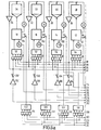
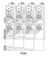
- FIGs. 6a and 6b show a system in which the peripheral equipment and the data link are protected by redundancy. Not all the measures taken in Figs. 6a and 6b need be implemented together and in the following the redundancy will be described as being implemented in stages.
- Fig. 6a - in particular the upper half - contains substantially the same elements as Fig. 3, again grouped in four error-isolation areas and numbered as in Fig. 3.
- the data link with the peripheral equipment is provided with the same measure of redundancy as the rest of the system.
- the peripheral equipment system is shown in Fig. 6b and will be discussed as and when applicable.
- the additions to Fig. 6a are concerned with the following :
- Figs. 6a and 6b that have not been described can be left out of the arrangement because the measures of Fig. 3 are applied to them : notably in Fig o 6b the elements 190, 192, 194 and their associated components and the element 260 are absent. In Fig. 6a the elements 308 - 322 are also absent.
- redundancy code On the next higher level of redundancy, the data transport over the lines in both directions is protected by a redundancy code.
- peripheral equipment takes place in blocks 188, 190, 192, 194, which themselves are conventional in nature and are not described further.
- the elements 172, 180, 188, 260, 268, 277 are in a single error-isolation area and the same is true for the other three-quarters of the circuit.
- Each peripheral equipment section has its own encoder 260, 262, 264, 266 to receive a data-word from the respective processing block 188, 190, 192, 194 and to generate a code-symbol.
- These code-symbol generators feed the lines 276, 278, 280, 282.
- Fig. 6b it is further assumed that each error-isolation area generates at most two control bits to the circuit of Fig. 6a.
- no encoder then needs to be included in the output lines for the control bits 300, 302, 304, 306, however there may be cases where this is indeed necessary.
- the lines 82, 84, 86, 88 can be combined in pairs with lines 276, 278, 280, 282 to constitute a full-duplex or a half-duplex operating bus.
- a larger number of peripheral equipments can be connected. It is then possible, for example, to use a "star" configuration for the control lines and a "bus" configuration for the data lines.
- a 16-bit data-word can also be coded into six symbols, each of four bits, because log 2 (5) is less than four. Less memory space is then necessary (24 bits per data-word, instead of 32 bits previously). It could also be done with eight symbols of three bits, but that does not yield less memory space and it can only correct one symbol of 3 bits.
- An 8-bit data-word can, if required, be coded as 5 symbols of 3 bits. This is done in that first a pseudo data-word of 9 bits (the last is a dummy bit or, e.g. a parity bit) is created and that is then coded. The memory capacity required is 6% less than that according to Fig. 3, but the calculations are somewhat more complicated.
- the method described above for the addition of redundancy is not restricted to protection against errors in only one error-isolation area. If a code-word contains more than two redundancy symbols, then more errors can be corrected.
- the MDS codes (minimum distance separable codes) used here have the property that the minimum distance between two symbols (Hamming distance) is equal to (n-k+1), where (n-k) is the number of redundancy symbols in a code-word.
- the data-word contains 4 symbols, each of 4 bits.
- the code-word contains 8 symbols, each of 4 bits.
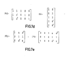
- the code is, for example, defined by the matrix [H] shown in Fig. 7a, where a is an element of GF(2 ).
- the processor is twelve-fold ; the redundancy in the memory involves a factor 1i.
- the code can correct one arbitrarily erroneous symbol of 1 bit.
- the code is defined, for example, by the parity matrix [H] shown in Fig. 7b and the generator matrix [GJ in Fig. 7c.
- the data-word thus contains two symbols of 2 bits.
- the code can detect a single symbol error and in the case that two symbols are erroneous it can detect this with 100% certainty. If on grounds of earlier data (statistics) the error locator of one of these two erroneous symbols is known, the other error can be corrected.
- the error locator of c * is numbered as follows (for the five symbols): (43210). If the known locator (i.e. of the"old” error) has the value 0, 1 or 2 then [H 1 ] is used, and only those rows on which the known error has no effect. If the known locator has the value "O”, only the upper two rows are thus used. If the known locator is "1”, only the odd rows, if it is "2", only the lower two rows. If the locator of the known error has the value "3" or "4", the matrix [H 2 ] is used with the corresponding syndrome. It has been shown that the device as illustrated in Fig.
- the reconstruction sections are controlled in one of two possible working modes:
- the parity matrix has the following form in which a is here one element of the Galois field GF(2 4 ):
- the generator matrix has the form:
- Generator matrix and parity matrix are implemented in the corresponding manner as described above.
- the replacement of a bit of arbitrary, but possibly erroneous, value by a logic "0" is easy to bring about, because the relevant bit is not used for the addressing of the read-only memory executing the information reconstruction.
- Switching from the "normal” mode to the "erase” mode can be done as follows: if a symbol error is corrected, an indication is given (see above) to show in which symbol, i.e. in which error-isolation area the fault has occurred. These indication signals are fed to a bookkeeping device. This may be a special processor, or even be embodied in processor means which, each time, are included in each error-isolation area. These are not indicated in the figures, but the processor, which is indicated , will usually have sufficient processing capacity. It is favourable therefore for the/processors to have means for reading out each other's error registers so as to learn errors detected by other error-isolation areas.
- an information reconstruction section can contain a read-only memory that is addressed by the entire code word and yields the desired information bits at its output.
- the selected information that indicates whether the system is working in the "normal” or the "erase” mode, " can together with the information (in Fig. 3, two bits) which indicates the "erased” error-isolation area, can function as additional address bits for this read-only memory.
Landscapes
- Engineering & Computer Science (AREA)
- Theoretical Computer Science (AREA)
- Physics & Mathematics (AREA)
- Quality & Reliability (AREA)
- General Engineering & Computer Science (AREA)
- General Physics & Mathematics (AREA)
- Probability & Statistics with Applications (AREA)
- Hardware Redundancy (AREA)
- Detection And Correction Of Errors (AREA)
- Error Detection And Correction (AREA)
- Multi Processors (AREA)
Priority Applications (1)
| Application Number | Priority Date | Filing Date | Title |
|---|---|---|---|
| AT80201185T ATE14250T1 (de) | 1979-12-20 | 1980-12-09 | Mehrrechner-datenverarbeitungssystem. |
Applications Claiming Priority (2)
| Application Number | Priority Date | Filing Date | Title |
|---|---|---|---|
| NL7909178 | 1979-12-20 | ||
| NL7909178A NL7909178A (nl) | 1979-12-20 | 1979-12-20 | Rekenmachine met verspreide redundantie welke is verdeeld over verschillende isolatiegebieden voor fouten. |
Publications (3)
| Publication Number | Publication Date |
|---|---|
| EP0031183A2 true EP0031183A2 (de) | 1981-07-01 |
| EP0031183A3 EP0031183A3 (en) | 1982-02-10 |
| EP0031183B1 EP0031183B1 (de) | 1985-07-10 |
Family
ID=19834353
Family Applications (1)
| Application Number | Title | Priority Date | Filing Date |
|---|---|---|---|
| EP80201185A Expired EP0031183B1 (de) | 1979-12-20 | 1980-12-09 | Mehrrechner-Datenverarbeitungssystem |
Country Status (8)
| Country | Link |
|---|---|
| US (1) | US4402045A (de) |
| EP (1) | EP0031183B1 (de) |
| JP (1) | JPS5697158A (de) |
| AT (1) | ATE14250T1 (de) |
| AU (1) | AU539375B2 (de) |
| CA (1) | CA1163373A (de) |
| DE (1) | DE3070868D1 (de) |
| NL (1) | NL7909178A (de) |
Cited By (3)
| Publication number | Priority date | Publication date | Assignee | Title |
|---|---|---|---|---|
| EP0075985A1 (de) * | 1981-09-21 | 1983-04-06 | Koninklijke Philips Electronics N.V. | Datenverarbeitungsvorrichtung zur Verarbeitung von Datenwörtern mit mehreren Symbolen, auf einem symbolkorrigierenden Kode basiert und mit mehreren Betriebsweisen |
| EP0110439A1 (de) * | 1982-10-20 | 1984-06-13 | Koninklijke Philips Electronics N.V. | Mehrrechner-Datenverarbeitungssystem welches n parallel arbeitende Datenverarbeitungsmodulen enthält und Datenverarbeitungsmodul zur Anwendung in einem solchen Mehrrechner-Datenverarbeitungssystem |
| FR2565002A1 (fr) * | 1984-05-25 | 1985-11-29 | Cii Honeywell Bull | Processeur de detection et de correction d'erreurs selon un code produit reed solomon entrelace |
Families Citing this family (40)
| Publication number | Priority date | Publication date | Assignee | Title |
|---|---|---|---|---|
| US4497059A (en) * | 1982-04-28 | 1985-01-29 | The Charles Stark Draper Laboratory, Inc. | Multi-channel redundant processing systems |
| NL8303536A (nl) * | 1983-10-14 | 1985-05-01 | Philips Nv | Geintegreerde schakeling op grote schaal welke verdeeld is in isochrone gebieden, werkwijze voor het machinaal ontwerpen van zo een geintegreerde schakeling, en werkwijze voor het machinaal testen van zo een geintegreerde schakeling. |
| NL8402472A (nl) * | 1984-08-10 | 1986-03-03 | Philips Nv | Multiprocessor-rekenmachinesysteem, bevattende n parallelwerkende rekenmachinemodules en voorzien van een extern apparaat, alsmede rekenmachinemodule voor gebruik in zo'n systeem. |
| US4751639A (en) * | 1985-06-24 | 1988-06-14 | Ncr Corporation | Virtual command rollback in a fault tolerant data processing system |
| NL8502768A (nl) * | 1985-10-10 | 1987-05-04 | Philips Nv | Dataverwerkingsinrichting, die uit meerdere, parallel-werkende dataverwerkingsmodules bestaat, multipel redundante klokinrichting, bevattende een aantal onderling zelf-synchroniserende klokschakelingen voor gebruik in zo een dataverwerkingsinrichting, en klokschakeling voor gebruik in zo een klokinrichting. |
| US4797848A (en) * | 1986-04-18 | 1989-01-10 | Hughes Aircraft Company | Pipelined bit-serial Galois Field multiplier |
| US4807228A (en) * | 1987-03-18 | 1989-02-21 | American Telephone And Telegraph Company, At&T Bell Laboratories | Method of spare capacity use for fault detection in a multiprocessor system |
| AU616213B2 (en) * | 1987-11-09 | 1991-10-24 | Tandem Computers Incorporated | Method and apparatus for synchronizing a plurality of processors |
| US5159686A (en) * | 1988-02-29 | 1992-10-27 | Convex Computer Corporation | Multi-processor computer system having process-independent communication register addressing |
| US5050070A (en) * | 1988-02-29 | 1991-09-17 | Convex Computer Corporation | Multi-processor computer system having self-allocating processors |
| US4891785A (en) * | 1988-07-08 | 1990-01-02 | Donohoo Theodore J | Method for transferring data files between computers in a network response to generalized application program instructions |
| US5201029A (en) * | 1988-10-24 | 1993-04-06 | U.S. Philips Corporation | Digital data processing apparatus using daisy chain control |
| AU625293B2 (en) * | 1988-12-09 | 1992-07-09 | Tandem Computers Incorporated | Synchronization of fault-tolerant computer system having multiple processors |
| US4965717A (en) * | 1988-12-09 | 1990-10-23 | Tandem Computers Incorporated | Multiple processor system having shared memory with private-write capability |
| US5295258A (en) * | 1989-12-22 | 1994-03-15 | Tandem Computers Incorporated | Fault-tolerant computer system with online recovery and reintegration of redundant components |
| US5203004A (en) * | 1990-01-08 | 1993-04-13 | Tandem Computers Incorporated | Multi-board system having electronic keying and preventing power to improperly connected plug-in board with improperly configured diode connections |
| DE69031947T2 (de) * | 1990-10-16 | 1998-07-16 | Koninkl Philips Electronics Nv | Datenverarbeitungssystem basierend auf einem (N,K)-Symbolkode und mit Symbolfehler-Korrigierbarkeit und mehrfacher Fehlerreparierbarkeit |
| US5257266A (en) * | 1991-02-27 | 1993-10-26 | General Dynamics Corporation, Space Systems Division | Computer and communications systems employing universal direct spherics processing architectures |
| US6141769A (en) | 1996-05-16 | 2000-10-31 | Resilience Corporation | Triple modular redundant computer system and associated method |
| US5956351A (en) * | 1997-04-07 | 1999-09-21 | International Business Machines Corporation | Dual error correction code |
| FR2794876B1 (fr) * | 1999-06-10 | 2001-11-02 | Bull Sa | Procede de reconfiguration d'un systeme de traitement de l'information sur detection de defaillance d'un composant |
| US6738935B1 (en) * | 2000-02-07 | 2004-05-18 | 3Com Corporation | Coding sublayer for multi-channel media with error correction |
| JP2003081060A (ja) * | 2001-09-11 | 2003-03-19 | Fujitsu Ten Ltd | キー閉じ込め防止装置 |
| US8832523B2 (en) * | 2006-03-03 | 2014-09-09 | Ternarylogic Llc | Multi-state symbol error correction in matrix based codes |
| US7007128B2 (en) * | 2004-01-07 | 2006-02-28 | International Business Machines Corporation | Multiprocessor data processing system having a data routing mechanism regulated through control communication |
| US7308558B2 (en) * | 2004-01-07 | 2007-12-11 | International Business Machines Corporation | Multiprocessor data processing system having scalable data interconnect and data routing mechanism |
| US8108429B2 (en) | 2004-05-07 | 2012-01-31 | Quest Software, Inc. | System for moving real-time data events across a plurality of devices in a network for simultaneous data protection, replication, and access services |
| US7565661B2 (en) | 2004-05-10 | 2009-07-21 | Siew Yong Sim-Tang | Method and system for real-time event journaling to provide enterprise data services |
| US7680834B1 (en) | 2004-06-08 | 2010-03-16 | Bakbone Software, Inc. | Method and system for no downtime resychronization for real-time, continuous data protection |
| US7681105B1 (en) * | 2004-08-09 | 2010-03-16 | Bakbone Software, Inc. | Method for lock-free clustered erasure coding and recovery of data across a plurality of data stores in a network |
| US7681104B1 (en) | 2004-08-09 | 2010-03-16 | Bakbone Software, Inc. | Method for erasure coding data across a plurality of data stores in a network |
| US7979404B2 (en) | 2004-09-17 | 2011-07-12 | Quest Software, Inc. | Extracting data changes and storing data history to allow for instantaneous access to and reconstruction of any point-in-time data |
| US7904913B2 (en) | 2004-11-02 | 2011-03-08 | Bakbone Software, Inc. | Management interface for a system that provides automated, real-time, continuous data protection |
| US7689602B1 (en) | 2005-07-20 | 2010-03-30 | Bakbone Software, Inc. | Method of creating hierarchical indices for a distributed object system |
| US7788521B1 (en) | 2005-07-20 | 2010-08-31 | Bakbone Software, Inc. | Method and system for virtual on-demand recovery for real-time, continuous data protection |
| US9203436B2 (en) * | 2006-07-12 | 2015-12-01 | Ternarylogic Llc | Error correction in multi-valued (p,k) codes |
| US8131723B2 (en) | 2007-03-30 | 2012-03-06 | Quest Software, Inc. | Recovering a file system to any point-in-time in the past with guaranteed structure, content consistency and integrity |
| US8364648B1 (en) | 2007-04-09 | 2013-01-29 | Quest Software, Inc. | Recovering a database to any point-in-time in the past with guaranteed data consistency |
| US9383970B2 (en) * | 2009-08-13 | 2016-07-05 | Microsoft Technology Licensing, Llc | Distributed analytics platform |
| CN105339905B (zh) * | 2013-04-09 | 2018-11-06 | 伊姆西公司 | 具有对大容量固态存储器资源的独立直接访问的多处理器系统 |
Family Cites Families (2)
| Publication number | Priority date | Publication date | Assignee | Title |
|---|---|---|---|---|
| DE2419587A1 (de) * | 1974-04-23 | 1975-11-06 | Siemens Ag | Schaltungsanordnung zum gesicherten verarbeiten von digital dargestellten informationen |
| IT1014277B (it) * | 1974-06-03 | 1977-04-20 | Cselt Centro Studi Lab Telecom | Sistema di controllo di elaboratori di processo operanti in parallelo |
-
1979
- 1979-12-20 NL NL7909178A patent/NL7909178A/nl not_active Application Discontinuation
-
1980
- 1980-12-09 DE DE8080201185T patent/DE3070868D1/de not_active Expired
- 1980-12-09 EP EP80201185A patent/EP0031183B1/de not_active Expired
- 1980-12-09 AT AT80201185T patent/ATE14250T1/de not_active IP Right Cessation
- 1980-12-11 CA CA000366572A patent/CA1163373A/en not_active Expired
- 1980-12-15 US US06/216,118 patent/US4402045A/en not_active Expired - Lifetime
- 1980-12-17 AU AU65447/80A patent/AU539375B2/en not_active Ceased
- 1980-12-19 JP JP18029380A patent/JPS5697158A/ja active Granted
Cited By (3)
| Publication number | Priority date | Publication date | Assignee | Title |
|---|---|---|---|---|
| EP0075985A1 (de) * | 1981-09-21 | 1983-04-06 | Koninklijke Philips Electronics N.V. | Datenverarbeitungsvorrichtung zur Verarbeitung von Datenwörtern mit mehreren Symbolen, auf einem symbolkorrigierenden Kode basiert und mit mehreren Betriebsweisen |
| EP0110439A1 (de) * | 1982-10-20 | 1984-06-13 | Koninklijke Philips Electronics N.V. | Mehrrechner-Datenverarbeitungssystem welches n parallel arbeitende Datenverarbeitungsmodulen enthält und Datenverarbeitungsmodul zur Anwendung in einem solchen Mehrrechner-Datenverarbeitungssystem |
| FR2565002A1 (fr) * | 1984-05-25 | 1985-11-29 | Cii Honeywell Bull | Processeur de detection et de correction d'erreurs selon un code produit reed solomon entrelace |
Also Published As
| Publication number | Publication date |
|---|---|
| EP0031183A3 (en) | 1982-02-10 |
| NL7909178A (nl) | 1981-07-16 |
| US4402045A (en) | 1983-08-30 |
| CA1163373A (en) | 1984-03-06 |
| DE3070868D1 (en) | 1985-08-14 |
| JPS5697158A (en) | 1981-08-05 |
| JPS6327734B2 (de) | 1988-06-06 |
| AU539375B2 (en) | 1984-09-27 |
| AU6544780A (en) | 1981-06-25 |
| ATE14250T1 (de) | 1985-07-15 |
| EP0031183B1 (de) | 1985-07-10 |
Similar Documents
| Publication | Publication Date | Title |
|---|---|---|
| US4402045A (en) | Multi-processor computer system | |
| US5226043A (en) | Apparatus and method for data error detection and correction and address error detection in a memory system | |
| US8099651B2 (en) | Subsystem and method for encoding 64-bit data nibble error correct and cyclic-redundancy code (CRC) address error detect for use in a 76-bit memory module | |
| US6453440B1 (en) | System and method for detecting double-bit errors and for correcting errors due to component failures | |
| US6675349B1 (en) | Error correction coding of data blocks with included parity bits | |
| US4512020A (en) | Data processing device for processing multiple-symbol data-words based on a symbol-correcting code and having multiple operating modes | |
| US6473880B1 (en) | System and method for protecting data and correcting bit errors due to component failures | |
| US4335458A (en) | Memory incorporating error detection and correction | |
| US5745508A (en) | Error-detection code | |
| US6604222B1 (en) | Block code to efficiently correct adjacent data and/or check bit errors | |
| US5856987A (en) | Encoder and decoder for an SEC-DED-S4ED rotational code | |
| US5778009A (en) | Dedicated ALU architecture for 10-bit Reed-Solomon error correction module | |
| JPS5960654A (ja) | エラ−訂正システム | |
| US3831144A (en) | Multi-level error detection code | |
| US7870473B2 (en) | Error detection device for an address decoder, and device for error detection for an address decoder | |
| JPS6349245B2 (de) | ||
| US5751745A (en) | Memory implemented error detection and correction code with address parity bits | |
| US6393597B1 (en) | Mechanism for decoding linearly-shifted codes to facilitate correction of bit errors due to component failures | |
| US5761221A (en) | Memory implemented error detection and correction code using memory modules | |
| US7093183B2 (en) | Symbol level error correction codes which protect against memory chip and bus line failures | |
| JP2732862B2 (ja) | データ伝送試験装置 | |
| JP3654655B2 (ja) | データ処理システム | |
| EP0178726B1 (de) | Datenverarbeitungssystem welches aufgebaut ist aus drei Datenverarbeitungsmodulen | |
| US8499224B2 (en) | Redundant code generation method and device, data restoration method and device, and raid storage device | |
| RU2297032C2 (ru) | Самокорректирующееся запоминающее устройство |
Legal Events
| Date | Code | Title | Description |
|---|---|---|---|
| PUAI | Public reference made under article 153(3) epc to a published international application that has entered the european phase |
Free format text: ORIGINAL CODE: 0009012 |
|
| AK | Designated contracting states |
Designated state(s): AT BE DE FR GB IT NL SE |
|
| PUAL | Search report despatched |
Free format text: ORIGINAL CODE: 0009013 |
|
| AK | Designated contracting states |
Designated state(s): AT BE DE FR GB IT NL SE |
|
| 17P | Request for examination filed |
Effective date: 19820111 |
|
| RAP1 | Party data changed (applicant data changed or rights of an application transferred) |
Owner name: N.V. PHILIPS' GLOEILAMPENFABRIEKEN |
|
| ITF | It: translation for a ep patent filed | ||
| GRAA | (expected) grant |
Free format text: ORIGINAL CODE: 0009210 |
|
| AK | Designated contracting states |
Designated state(s): AT BE DE FR GB IT NL SE |
|
| REF | Corresponds to: |
Ref document number: 14250 Country of ref document: AT Date of ref document: 19850715 Kind code of ref document: T |
|
| REF | Corresponds to: |
Ref document number: 3070868 Country of ref document: DE Date of ref document: 19850814 |
|
| ET | Fr: translation filed | ||
| PLBE | No opposition filed within time limit |
Free format text: ORIGINAL CODE: 0009261 |
|
| STAA | Information on the status of an ep patent application or granted ep patent |
Free format text: STATUS: NO OPPOSITION FILED WITHIN TIME LIMIT |
|
| 26N | No opposition filed | ||
| PGFP | Annual fee paid to national office [announced via postgrant information from national office to epo] |
Ref country code: NL Payment date: 19891231 Year of fee payment: 10 |
|
| PG25 | Lapsed in a contracting state [announced via postgrant information from national office to epo] |
Ref country code: NL Effective date: 19910701 |
|
| NLV4 | Nl: lapsed or anulled due to non-payment of the annual fee | ||
| ITTA | It: last paid annual fee | ||
| EAL | Se: european patent in force in sweden |
Ref document number: 80201185.8 |
|
| ITPR | It: changes in ownership of a european patent |
Owner name: CAMBIO RAGIONE SOCIALE;PHILIPS ELECTRONICS N.V. |
|
| REG | Reference to a national code |
Ref country code: FR Ref legal event code: CD |
|
| REG | Reference to a national code |
Ref country code: FR Ref legal event code: CD |
|
| PGFP | Annual fee paid to national office [announced via postgrant information from national office to epo] |
Ref country code: BE Payment date: 19981201 Year of fee payment: 19 |
|
| PGFP | Annual fee paid to national office [announced via postgrant information from national office to epo] |
Ref country code: GB Payment date: 19981218 Year of fee payment: 19 |
|
| PGFP | Annual fee paid to national office [announced via postgrant information from national office to epo] |
Ref country code: FR Payment date: 19981222 Year of fee payment: 19 Ref country code: AT Payment date: 19981222 Year of fee payment: 19 |
|
| PGFP | Annual fee paid to national office [announced via postgrant information from national office to epo] |
Ref country code: SE Payment date: 19981223 Year of fee payment: 19 |
|
| PGFP | Annual fee paid to national office [announced via postgrant information from national office to epo] |
Ref country code: DE Payment date: 19990217 Year of fee payment: 19 |
|
| PG25 | Lapsed in a contracting state [announced via postgrant information from national office to epo] |
Ref country code: GB Free format text: LAPSE BECAUSE OF NON-PAYMENT OF DUE FEES Effective date: 19991209 Ref country code: AT Free format text: LAPSE BECAUSE OF NON-PAYMENT OF DUE FEES Effective date: 19991209 |
|
| PG25 | Lapsed in a contracting state [announced via postgrant information from national office to epo] |
Ref country code: SE Free format text: LAPSE BECAUSE OF NON-PAYMENT OF DUE FEES Effective date: 19991210 |
|
| PG25 | Lapsed in a contracting state [announced via postgrant information from national office to epo] |
Ref country code: BE Free format text: LAPSE BECAUSE OF NON-PAYMENT OF DUE FEES Effective date: 19991231 |
|
| BERE | Be: lapsed |
Owner name: KONINKLIJKE PHILIPS ELECTRONICS N.V. Effective date: 19991231 |
|
| GBPC | Gb: european patent ceased through non-payment of renewal fee |
Effective date: 19991209 |
|
| EUG | Se: european patent has lapsed |
Ref document number: 80201185.8 |
|
| PG25 | Lapsed in a contracting state [announced via postgrant information from national office to epo] |
Ref country code: FR Free format text: LAPSE BECAUSE OF NON-PAYMENT OF DUE FEES Effective date: 20000831 |
|
| PG25 | Lapsed in a contracting state [announced via postgrant information from national office to epo] |
Ref country code: DE Free format text: LAPSE BECAUSE OF NON-PAYMENT OF DUE FEES Effective date: 20001003 |
|
| REG | Reference to a national code |
Ref country code: FR Ref legal event code: ST |