EP0031685B1 - Dispositif à ondes acoustiques de surface - Google Patents
Dispositif à ondes acoustiques de surface Download PDFInfo
- Publication number
- EP0031685B1 EP0031685B1 EP80304604A EP80304604A EP0031685B1 EP 0031685 B1 EP0031685 B1 EP 0031685B1 EP 80304604 A EP80304604 A EP 80304604A EP 80304604 A EP80304604 A EP 80304604A EP 0031685 B1 EP0031685 B1 EP 0031685B1
- Authority
- EP
- European Patent Office
- Prior art keywords
- dummy
- substrate
- transducers
- input
- transducer
- Prior art date
- Legal status (The legal status is an assumption and is not a legal conclusion. Google has not performed a legal analysis and makes no representation as to the accuracy of the status listed.)
- Expired
Links
Images



Classifications
-
- H—ELECTRICITY
- H03—ELECTRONIC CIRCUITRY
- H03H—IMPEDANCE NETWORKS, e.g. RESONANT CIRCUITS; RESONATORS
- H03H9/00—Networks comprising electromechanical or electro-acoustic elements; Electromechanical resonators
- H03H9/02—Details
- H03H9/02535—Details of surface acoustic wave devices
- H03H9/02637—Details concerning reflective or coupling arrays
- H03H9/02685—Grating lines having particular arrangements
- H03H9/02771—Reflector banks
-
- H—ELECTRICITY
- H03—ELECTRONIC CIRCUITRY
- H03H—IMPEDANCE NETWORKS, e.g. RESONANT CIRCUITS; RESONATORS
- H03H9/00—Networks comprising electromechanical or electro-acoustic elements; Electromechanical resonators
- H03H9/02—Details
- H03H9/02535—Details of surface acoustic wave devices
- H03H9/02818—Means for compensation or elimination of undesirable effects
- H03H9/02842—Means for compensation or elimination of undesirable effects of reflections
-
- H—ELECTRICITY
- H03—ELECTRONIC CIRCUITRY
- H03H—IMPEDANCE NETWORKS, e.g. RESONANT CIRCUITS; RESONATORS
- H03H9/00—Networks comprising electromechanical or electro-acoustic elements; Electromechanical resonators
- H03H9/02—Details
- H03H9/125—Driving means, e.g. electrodes, coils
- H03H9/145—Driving means, e.g. electrodes, coils for networks using surface acoustic waves
- H03H9/14544—Transducers of particular shape or position
- H03H9/14573—Arrow type transducers
-
- H—ELECTRICITY
- H03—ELECTRONIC CIRCUITRY
- H03H—IMPEDANCE NETWORKS, e.g. RESONANT CIRCUITS; RESONATORS
- H03H9/00—Networks comprising electromechanical or electro-acoustic elements; Electromechanical resonators
- H03H9/02—Details
- H03H9/02535—Details of surface acoustic wave devices
- H03H9/02818—Means for compensation or elimination of undesirable effects
- H03H9/02866—Means for compensation or elimination of undesirable effects of bulk wave excitation and reflections
-
- H—ELECTRICITY
- H03—ELECTRONIC CIRCUITRY
- H03H—IMPEDANCE NETWORKS, e.g. RESONANT CIRCUITS; RESONATORS
- H03H9/00—Networks comprising electromechanical or electro-acoustic elements; Electromechanical resonators
- H03H9/02—Details
- H03H9/125—Driving means, e.g. electrodes, coils
- H03H9/145—Driving means, e.g. electrodes, coils for networks using surface acoustic waves
- H03H9/14544—Transducers of particular shape or position
- H03H9/14547—Fan shaped; Tilted; Shifted; Slanted; Tapered; Arched; Stepped finger transducers
Definitions
- the present invention relates to a surface acoustic wave device.
- Fig. 1 illustrates a fundamental construction of a surface acoustic wave device serving as a band pass filter.
- This surface acoustic wave device comprises a substrate 1, which is made of a piezoelectric material, such as lithium niobate (LiNb0 3 ) or lithium tantalate (KiTa0 3 ), and is provided on the surface thereof with an input transducer 2 and an output transducer 3, each of which is composed of a pair of interdigitated comb-like electrodes made of a thin film of metal.
- a substrate 1 which is made of a piezoelectric material, such as lithium niobate (LiNb0 3 ) or lithium tantalate (KiTa0 3 )
- an input transducer 2 and an output transducer 3 each of which is composed of a pair of interdigitated comb-like electrodes made of a thin film of metal.
- the electrodes of the input transducer 2 When electrical signals from a generator 4 are applied to the electrodes of the input transducer 2, the latter emits surface acoustic waves 5, which are propagated to the output transducer 3 and then converted into other electrical signals which can be taken out from a load impedance 6.
- the electrodes of the input and output transducers can be designed in a variety of patterns, so as to provide various desired characteristics to the filter when electrical signals are converted into acoustic signals or vice versa.
- the input transducer emits bulk waves, in addition to surface acoustic waves, which bulk waves are propagated through the body of the substrate to reach the output transducer, thereby adversely affecting the output characteristics of the latter.
- the input transducer 2 and the output transducer 3 are arranged diagonally opposite each other, and a multistrip coupler 7 which includes a plurality of parallel conductors is provided between the input and output transducers. According to this arrangement, the path of propagation of the surface acoustic waves is changed as indicated by a solid arrow, as a result, the effect of the bulk waves which are propagated as indicated by a dotted arrow, is eliminated.
- a surface acoustic wave device comprising a piezoelectric substrate, and input and output transducers formed on said substrate and being individually composed of a pair of comb-like electrodes, wherein said device further comprises dummy transducers formed on said substrate and arranged to extend from the outer ends of said input and output transducers toward the ends of said substrate, respectively, said dummy transducers individually including a plurality of electrodes spaced at substantially the same pitch as the electrode pitch in the respective input and output transducers.
- a surface acoustic wave device comprising a piezoelectric substrate, input and output transducers formed on said substrate and arranged diagonally opposite each other, said input and output transducers individually being composed of a pair of comb-like electrodes, and a multistrip coupler formed on said substrate and inter-posed between said input and output transducers and including a plurality of filamentary conductors, wherein said device further comprises dummy transducers formed on said substrate and arranged to extend from the outer ends of said input and output transducers toward the ends of said substrate, respectively, said dummy transducers individually including a plurality of electrodes spaced at substantially the same pitch as the electrode pitch in the respective input and output transducers.
- the device according to another embodiment of the present invention further comprises dummy transducers formed on said substrate and arranged to extend from the opposite ends of said multistrip coupler toward the ends of said substrate, respectively, said dummy transducers individually including a plurality of electrodes spaced at substantially the same pitch as the conductor pitch of said multistrip coupler.
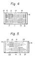
- a first embodiment of a surface acoustic wave device comprises a substrate 11 which is made of a piezoelectric material.
- the substrate 11 is provided on a plane surface thereof with an input transducer 12, an output transducer 13, a multistrip coupler 14, and dummy transducers 15, 16, 17 and 18, which elements are formed, for example, by etching a vapor deposited thin film of aluminum by means of photolithographic technology.
- the input transducer 12 and the output transducer 13 are arranged diagonally opposite to each other with the multistrip coupler 14 therebetween.
- Each of the input and output transducers 12 and 13 is composed of a pair of interdigitated comb-like electrodes and has a construction in which the pitch (i.e. center-to- center spacing) of the electrodes is about A/4 and the width of the electrodes is about A/8, where A is a wavelength at the center frequency of the surface acoustic wave.
- the multistrip coupler 14 is arranged so as to be substantially orthogonal to the propagation direction of the surface acoustic wave, and includes a plurality of parallel filamentary conductors.
- the dummy transducer 15 is arranged to extend from the outer end of the input transducer 12 towards one end of the substrate 11 and includes a plurality of electrodes spaced at substantially the same pitch as the electrode pitch in the input transducer 12.
- the dummy transducer 1 is arranged to extend from the outer end of the output transducer 13 toward the opposite end of the substrate 11 and includes a plurality of electrodes spaced at substantially the same pitch as the electrode pitch in the output transducer 13.
- the dummy transducers 17 and 18 are arranged to extend from the opposite ends of the multistrip coupler 14 toward the opposite ends of the substrate 11, respectively and each includes a plurality of electrodes spaced at substantially the same pitch as the conductor pitch in the multistrip coupler 14.
- the opposite ends of the substrate 11 are applied with acoustic absorption materials 19, such as phenolic resin or oleoresin, for example, which cover the outer end portions of the dummy transducers 15 through 18.
- the surface acoustic waves reaching the ends of the multistrip coupler 14 and the output transducer 13 are then propagated through the dummy transducers 18 and 16, respectively, and, finally, absorbed by the acoustic absorption material 19.
- the other dummy transducers 15 and 17 also provide substantially the same effects as mentioned above.
- a second embodiment of the present invention is basically similar to the first embodiment described previously, but comprises, instead of the dummy transducers 15 through 18, dummy transducers 20, 21, 22 and 23.
- the electrodes of the individual dummy transducers 20 through 23 are formed to be successively shorter in length toward the end of the substrate 11, so that each individual dummy transducer is formed in the shape of a rope end.
- the surface acoustic waves reaching the ends of the multistrip coupler 14 and the output transducer 13 are propagated through the dummy transducers 23 and 21, respectively, and, then, are dampered gradually due to the slight reflections from the successively varied lengths of the electrodes of the dummy transducers. Therefore, as in the first embodiment mentioned previously, there is no occurrence of the reflections of the surface acoustic wave from the ends of the multistrip coupler 14 and the output transducer 13, respectively.
- Figs. 7 through 9 are oscillograms of reflected waves in an experiment, in which a pulse 24 illustrated in Fig. 6 is applied to the conventional filter in Fig. 2 and the first and second embodiments of the present invention in Figs. 4 and 5.
- the reflected wave in the conventional filter in Fig. 2 includes a reflection 25 from the inner end of the input transducer, a reflection 26 from the end of the multistrip coupler, a reflection 27 from the outer end of the output transducer and a reflection 28 from the entire output transducer.
- both reflected waves in the first and second embodiments of the present invention do not include the reflections 26 and 27 from the end of the multistrip coupler and the output transducer.
- a third embodiment of the present invention comprises a piezoelectric substrate 31 which is provided on the surface thereof with an input transducer 32, an output transducer 33, a multistrip coupler 34, dummy transducers 35 and 36 and dummy couplers 37 and 38.
- the input and output transducers 32 and 33 and the multistrip coupler 34 are basically similar to those in the conventional device mentioned previously, but the electrodes of the input and output transducers 32 and 33 are weighted to provide desired frequency characteristics.
- the dummy transducer 35 is arranged to extend from the outer end of the input transducer 33 toward the end of the substrate 31 and includes a plurality of electrodes spaced at substantially the same pitch as the electrode pitch in the input transducer 32.
- the dummy transducer 36 is arranged to extend from the outer end of the output transducer 33 towards the end of the substrate 31 and includes a plurality of electrodes spaced at substantially the same pitch as the electrode pitch in the output transducer 33.
- the dummy coupler 37 is interposed between the input transducer 32 and the multistrip coupler 34 and includes a plurality of conductors spaced at substantially the same pitch as the electrode pitch of the input transducer 32 or the conductor pitch of the multistrip coupler 34.
- the dummy coupler 38 is interposed between the output transducer 33 and the multistrip coupler 34 and includes a plurality of conductors spaced at substantially the same pitch as the electrode pitch of the output transducer 33 or the conductor pitch of the multistrip coupler 34.
- the opposed ends of the substrate 31 is applied with acoustic absorption materials 39, such as phenolic resin or oleoresin, which cover the outer end portions of the dummy transducers 35 and 36.
- each of the electrodes of the dummy transducer 35 is connected by the opposed lateral ends to the electrode terminals 32a and 32b of the input transducer 32, and each of the electrodes of the dummy transducer 36 is connected by the opposite lateral ends to the electrode terminals 33a and 33b of the output transducer 33.
- either or both of the opposed lateral ends of each electrode of the dummy transducer may be opened.
- Fig. 11 illustrates a variation 36a of the dummy transducer 36, in which only one lateral end of each electrode is connected to the terminal 33a.
- Fig. 12 illustrates another variation 36b of the dummy transducer 36, in which both lateral ends of each electrode are opened.
- the surface acoustic wave reaching the end of the output transducer 33 is propagated through the dummy transducer 36 and, then, absorbed by the acoustic absorption material 39. Therefore, there is no occurrence of the reflection of the surface acoustic wave from the end of the output transducer 33. Furthermore, the surface acoustic wave reaching the inner end of the input transducer 32 is propagated through the dummy coupler 37 to the multistrip coupler 34, and accordingly the reflection 25 from the inner end of the input transducer as illustrated in Figs. 7 through 9 is prevented from occurring.
- the dummy transducer 35 and the dummy coupler 38 provides substantially the same effects as mentioned above.
- the frequency characteristics of the third embodiment of the present invention in Fig. 10 will be described below, in comparison with that of a conventional device similar to this third embodiment, but without the dummy transducers 35 and 36 and without the dummy couplers 37 and 38.
- Each of the device of the present invention and the conventional device has a center frequency of 36 MHz and a frequency band of 7 MHz, and is constructed with the following dimensions.
- the acoustic absorption material 39 for example, phenolic resin can be applied according to the experimental results illustrated in Fig. 13.
- the curvers 41 (dotted line) and 42 (chain-dotted line) were obtained when the thickness of the acoustic absorption material A is of 22 ⁇ and of more than 50,u, respectively.
- the 2.5ps reflection level is approximately constant.
- Figs. 14 and 14A and Figs. 15 and 15A The frequency characteristics of the conventional device and the device of the present invention, constructed as mentioned above, are illustrated in Figs. 14 and 14A and Figs. 15 and 15A, respectively.
- the abscissa represents the frequency
- the left ordinate represents the amplitude in relation with a curve 51 or 61
- the right ordinate represents the group delay in relation with a curve 52 or 62.
- Figs. 14A and 15A illustrate the portions 51 A and 61 A of the curves 51 and 61 in the Figs. 14 and 15, respectively, with a magnified scale of ordinate. It will be understood from these figures that the ripples of the amplitude and group delay are large in the conventional device, and, contrary to this, small in the device of the present invention, accordingly good frequency characteristics can be provided.
Landscapes
- Physics & Mathematics (AREA)
- Acoustics & Sound (AREA)
- Surface Acoustic Wave Elements And Circuit Networks Thereof (AREA)
Claims (11)
Applications Claiming Priority (2)
| Application Number | Priority Date | Filing Date | Title |
|---|---|---|---|
| JP16919079A JPS5693414A (en) | 1979-12-27 | 1979-12-27 | Elastic surface wave element |
| JP160190/79 | 1979-12-27 |
Publications (4)
| Publication Number | Publication Date |
|---|---|
| EP0031685A2 EP0031685A2 (fr) | 1981-07-08 |
| EP0031685A3 EP0031685A3 (en) | 1981-10-07 |
| EP0031685B1 true EP0031685B1 (fr) | 1984-02-29 |
| EP0031685B2 EP0031685B2 (fr) | 1990-06-27 |
Family
ID=15881891
Family Applications (1)
| Application Number | Title | Priority Date | Filing Date |
|---|---|---|---|
| EP80304604A Expired EP0031685B2 (fr) | 1979-12-27 | 1980-12-18 | Dispositif à ondes acoustiques de surface |
Country Status (4)
| Country | Link |
|---|---|
| US (1) | US4350963A (fr) |
| EP (1) | EP0031685B2 (fr) |
| JP (1) | JPS5693414A (fr) |
| DE (1) | DE3066777D1 (fr) |
Families Citing this family (12)
| Publication number | Priority date | Publication date | Assignee | Title |
|---|---|---|---|---|
| JPS57127321A (en) | 1981-01-30 | 1982-08-07 | Fujitsu Ltd | Surface acoustic wave filter |
| US4393358A (en) * | 1981-11-18 | 1983-07-12 | Zenith Radio Corporation | Surface wave acoustic device with compensation for diffraction effects |
| EP0097642A1 (fr) * | 1981-12-14 | 1984-01-11 | Gte Products Corporation | Cire acoustique sur un dispositif a ondes de surface |
| US4450420A (en) * | 1982-01-13 | 1984-05-22 | Gte Products Corporation | Surface acoustic wave filter |
| US4472694A (en) * | 1982-09-07 | 1984-09-18 | Gte Laboratories Incorporated | Acoustic surface wave device |
| GB2157522B (en) * | 1984-04-09 | 1987-08-19 | Philips Electronic Associated | Electrical filter comprising an acoustic surface wave device, and method of manufacturing such a filter |
| GB2160379A (en) * | 1984-06-15 | 1985-12-18 | Philips Electronic Associated | Surface-propagating acoustic wave device |
| CA1254994A (fr) * | 1985-03-29 | 1989-05-30 | Mark S. Suthers | Dispositifs a ondes acoustiques de surface a languettes d'elimination des reflexions |
| EP0584761B2 (fr) * | 1992-08-24 | 2005-08-31 | NRS Technologies Inc. | Filtre à résonateurs à ondes acoustiques de surface |
| US5363073A (en) * | 1992-10-19 | 1994-11-08 | Motorola, Inc. | Saw resonator filter with a multistrip coupler disposed in the resonator gaps |
| JP3512777B2 (ja) * | 2000-04-24 | 2004-03-31 | 三菱電機株式会社 | 縦結合型弾性表面波フィルタ |
| US6967545B2 (en) * | 2000-11-29 | 2005-11-22 | Yuri Abramov | Saw wave-guides |
Family Cites Families (5)
| Publication number | Priority date | Publication date | Assignee | Title |
|---|---|---|---|---|
| US4004254A (en) * | 1975-04-03 | 1977-01-18 | Zenith Radio Corporation | Swif with side lobe compensation barrier |
| US4096455A (en) * | 1977-02-23 | 1978-06-20 | Tektronix, Inc. | Surface wave termination for saw device |
| US4146851A (en) * | 1977-06-23 | 1979-03-27 | Gte Laboratories Incorporated | Acoustic surface wave device |
| DE2839851C2 (de) * | 1978-09-13 | 1980-09-25 | Siemens Ag, 1000 Berlin Und 8000 Muenchen | Oberflächenwellenanordnung mit verbesserter Störsignalunterdrückung |
| JPS5937605B2 (ja) * | 1979-09-25 | 1984-09-11 | 富士通株式会社 | 弾性表面波素子 |
-
1979
- 1979-12-27 JP JP16919079A patent/JPS5693414A/ja active Pending
-
1980
- 1980-12-18 EP EP80304604A patent/EP0031685B2/fr not_active Expired
- 1980-12-18 DE DE8080304604T patent/DE3066777D1/de not_active Expired
- 1980-12-24 US US06/219,948 patent/US4350963A/en not_active Expired - Lifetime
Also Published As
| Publication number | Publication date |
|---|---|
| EP0031685A3 (en) | 1981-10-07 |
| DE3066777D1 (en) | 1984-04-05 |
| EP0031685A2 (fr) | 1981-07-08 |
| JPS5693414A (en) | 1981-07-29 |
| US4350963A (en) | 1982-09-21 |
| EP0031685B2 (fr) | 1990-06-27 |
Similar Documents
| Publication | Publication Date | Title |
|---|---|---|
| US3961293A (en) | Multi-resonant surface wave resonator | |
| CA1180436A (fr) | Resonateur pour ondes acoustiques de surface | |
| CA1047615A (fr) | Filtre d'ondes acoustiques de surface | |
| US4353046A (en) | Surface acoustic wave device with reflectors | |
| US4162465A (en) | Surface acoustic wave device with reflection suppression | |
| US3980904A (en) | Elastic surface wave device | |
| US4350963A (en) | Surface acoustic wave device | |
| US4454488A (en) | Surface acoustic wave resonator with middle grating | |
| EP0026114A1 (fr) | Dispositif à ondes acoustiques de surface | |
| US3987376A (en) | Acoustic surface wave device with harmonic coupled transducers | |
| US5977846A (en) | Unidirectional surface acoustic wave filter | |
| US4097825A (en) | Surface acoustic wave tapped delay line | |
| US5136266A (en) | Surface acoustic wave device having staggered dispersive delay transducers | |
| US4354129A (en) | Absorber for piezoelectric surface acoustic wave device | |
| EP0579871A1 (fr) | Convolutionneur d'ondes acoustiques de surface | |
| US3870975A (en) | Surface wave transducer with reduced reflection coefficient | |
| US4263569A (en) | Surface acoustic wave arrangement with improved suppression of spurious signals | |
| GB1604186A (en) | Acoustic surface wave device | |
| KR100221230B1 (ko) | 자유단선 반사형 표면 음향파 장치 | |
| US4365220A (en) | Surface wave circuit device | |
| US4205285A (en) | Acoustic surface wave device | |
| US4346322A (en) | Elastic surface wave device | |
| GB2097212A (en) | Acoustic wave bandpass electrical filters | |
| EP0057598A2 (fr) | Dispositif à ondes acoustiques de surface | |
| JPH0356014B2 (fr) |
Legal Events
| Date | Code | Title | Description |
|---|---|---|---|
| PUAI | Public reference made under article 153(3) epc to a published international application that has entered the european phase |
Free format text: ORIGINAL CODE: 0009012 |
|
| 17P | Request for examination filed |
Effective date: 19810209 |
|
| AK | Designated contracting states |
Designated state(s): DE FR GB |
|
| PUAL | Search report despatched |
Free format text: ORIGINAL CODE: 0009013 |
|
| AK | Designated contracting states |
Designated state(s): DE FR GB |
|
| GRAA | (expected) grant |
Free format text: ORIGINAL CODE: 0009210 |
|
| AK | Designated contracting states |
Designated state(s): DE FR GB |
|
| REF | Corresponds to: |
Ref document number: 3066777 Country of ref document: DE Date of ref document: 19840405 |
|
| ET | Fr: translation filed | ||
| PLBI | Opposition filed |
Free format text: ORIGINAL CODE: 0009260 |
|
| 26 | Opposition filed |
Opponent name: N.V. PHILIPS' GLOEILAMPENFABRIEKEN Effective date: 19841122 |
|
| PUAH | Patent maintained in amended form |
Free format text: ORIGINAL CODE: 0009272 |
|
| STAA | Information on the status of an ep patent application or granted ep patent |
Free format text: STATUS: PATENT MAINTAINED AS AMENDED |
|
| 27A | Patent maintained in amended form |
Effective date: 19900627 |
|
| AK | Designated contracting states |
Kind code of ref document: B2 Designated state(s): DE FR GB |
|
| ET3 | Fr: translation filed ** decision concerning opposition | ||
| PGFP | Annual fee paid to national office [announced via postgrant information from national office to epo] |
Ref country code: GB Payment date: 19951211 Year of fee payment: 16 |
|
| PGFP | Annual fee paid to national office [announced via postgrant information from national office to epo] |
Ref country code: FR Payment date: 19951212 Year of fee payment: 16 |
|
| PGFP | Annual fee paid to national office [announced via postgrant information from national office to epo] |
Ref country code: DE Payment date: 19951222 Year of fee payment: 16 |
|
| APAC | Appeal dossier modified |
Free format text: ORIGINAL CODE: EPIDOS NOAPO |
|
| APAC | Appeal dossier modified |
Free format text: ORIGINAL CODE: EPIDOS NOAPO |
|
| PG25 | Lapsed in a contracting state [announced via postgrant information from national office to epo] |
Ref country code: GB Effective date: 19961218 |
|
| GBPC | Gb: european patent ceased through non-payment of renewal fee |
Effective date: 19961218 |
|
| PG25 | Lapsed in a contracting state [announced via postgrant information from national office to epo] |
Ref country code: FR Effective date: 19970829 |
|
| PG25 | Lapsed in a contracting state [announced via postgrant information from national office to epo] |
Ref country code: DE Effective date: 19970902 |
|
| REG | Reference to a national code |
Ref country code: FR Ref legal event code: ST |
|
| APAH | Appeal reference modified |
Free format text: ORIGINAL CODE: EPIDOSCREFNO |