EP0031995B1 - Halbleiterspeicheranordnung mit matrixartig angeordneten statischen Speicherzellen - Google Patents
Halbleiterspeicheranordnung mit matrixartig angeordneten statischen Speicherzellen Download PDFInfo
- Publication number
- EP0031995B1 EP0031995B1 EP80304189A EP80304189A EP0031995B1 EP 0031995 B1 EP0031995 B1 EP 0031995B1 EP 80304189 A EP80304189 A EP 80304189A EP 80304189 A EP80304189 A EP 80304189A EP 0031995 B1 EP0031995 B1 EP 0031995B1
- Authority
- EP
- European Patent Office
- Prior art keywords
- amplifier circuit
- ram device
- latch amplifier
- memory cells
- latch
- Prior art date
- Legal status (The legal status is an assumption and is not a legal conclusion. Google has not performed a legal analysis and makes no representation as to the accuracy of the status listed.)
- Expired
Links
Images

Classifications
-
- G—PHYSICS
- G11—INFORMATION STORAGE
- G11C—STATIC STORES
- G11C11/00—Digital stores characterised by the use of particular electric or magnetic storage elements; Storage elements therefor
- G11C11/21—Digital stores characterised by the use of particular electric or magnetic storage elements; Storage elements therefor using electric elements
- G11C11/34—Digital stores characterised by the use of particular electric or magnetic storage elements; Storage elements therefor using electric elements using semiconductor devices
- G11C11/40—Digital stores characterised by the use of particular electric or magnetic storage elements; Storage elements therefor using electric elements using semiconductor devices using transistors
- G11C11/41—Digital stores characterised by the use of particular electric or magnetic storage elements; Storage elements therefor using electric elements using semiconductor devices using transistors forming static cells with positive feedback, i.e. cells not needing refreshing or charge regeneration, e.g. bistable multivibrator or Schmitt trigger
- G11C11/413—Auxiliary circuits, e.g. for addressing, decoding, driving, writing, sensing, timing or power reduction
- G11C11/417—Auxiliary circuits, e.g. for addressing, decoding, driving, writing, sensing, timing or power reduction for memory cells of the field-effect type
- G11C11/419—Read-write [R-W] circuits
-
- G—PHYSICS
- G11—INFORMATION STORAGE
- G11C—STATIC STORES
- G11C11/00—Digital stores characterised by the use of particular electric or magnetic storage elements; Storage elements therefor
- G11C11/21—Digital stores characterised by the use of particular electric or magnetic storage elements; Storage elements therefor using electric elements
- G11C11/34—Digital stores characterised by the use of particular electric or magnetic storage elements; Storage elements therefor using electric elements using semiconductor devices
- G11C11/40—Digital stores characterised by the use of particular electric or magnetic storage elements; Storage elements therefor using electric elements using semiconductor devices using transistors
- G11C11/41—Digital stores characterised by the use of particular electric or magnetic storage elements; Storage elements therefor using electric elements using semiconductor devices using transistors forming static cells with positive feedback, i.e. cells not needing refreshing or charge regeneration, e.g. bistable multivibrator or Schmitt trigger
- G11C11/412—Digital stores characterised by the use of particular electric or magnetic storage elements; Storage elements therefor using electric elements using semiconductor devices using transistors forming static cells with positive feedback, i.e. cells not needing refreshing or charge regeneration, e.g. bistable multivibrator or Schmitt trigger using field-effect transistors only
Definitions
- the present invention relates to a semiconductor RAM (Random Access Memory) device, more particularly to a static-type RAM device.
- a semiconductor RAM Random Access Memory
- a semiconductor memory having a sense amplifier, or latch is disclosed in US-A-3879621, in which a plurality of row lines permits the selection of individual memory cells of a column of memory cells for read-out.
- the sense amplifier is connected to bit lines of the column through gate circuits.
- the bit lines are precharged and the gate circuits, in response to control signal, couple the sense amplifier to the bit lines, so that the sense amplifier .tracks the bit line potential when a bit line is discharged by the selection of a memory cell by a row line. Thereafter, the gate circuits disconnect the sense amplifier from the bit lines, and thereby isolate the bit lines.
- the amplitude of a read-out signal from a memory cell becomes small, so that the reliability of the read-out data is decreased; and the time necessary to change the potential on each of the bit lines and the data bus lines becomes large, because it takes a long time to charge or discharge the stray capacitance of these lines by a memory cell having a small drive capacity. Therefore, the read-out time of the RAM device increases according to the increase in the integration degree of the RAM device.
- the present invention consists in a semiconductor RAM device having a plurality of static-type memory cells which are disposed in a matrix of rows and columns and each of which is selected by an output from a row decoder and an output from a column decoder in response to input address signals and comprising a latch amplifier circuit coupled to the memory cells through gate circuits which are operated by a control pulse so that the latch amplifier circuit receives, through the gate circuits a data signal corresponding to the state of a selected memory cell, characterized in that a separate latch amplifier circuit is provided for each column and in that the device further comprises a control pulse generating circuit which, in response to a potential change of at least one of the input address signals, generates the control pulse after a predetermined delay, and in that the latch amplifier circuit is activated after the data signal has been fed to the latch amplifier circuit through the gate circuits under the control of the control pulse.
- the amplifier circuits have a larger drive capacity than that of the memory cells, so as to prevent the slow down of the read-out speed of such a device
- Fig. 1 illustrates a static type semiconductor RAM device in accordance with an embodiment of the present invention.
- memory cells MC 00 through MC NN are disposed in a matrix of N rows by N columns and each of the memory cells consists mainly of a flip-flop, which will be explained later in detail.
- Word lines W o through W N are connected to X address (or row address) decoders XD o through XD N respectively, and each of the word lines W o through W N is selected by corresponding one of the output signals X o through X N from the X address decoders XD o through XD N .
- a plurality of bit line pairs B o , B o through B N , B N are crossed with a plurality of the word lines W o through W N to form the matrix.
- one of the memory cells MC oo through MC NN is connected between a bit line pair and a word line.
- These bit line pairs B 0 , B 0 through B N , B N are connected to latch circuits or amplifier circuits RA o through RA N respectively, according to the present invention. All the latch circuits RA 0 through RA N have the same structure, and therefore only the latch circuit RA 0 will be explained hereinafter.
- the latch circuit RA 0 comprises load transistors Q 1 , Q 2 and driver transistors Q 3 , Q 4 which compose a flip-flop.
- the latch circuit RA 0 further comprises gate transistors Q 5 and Q 6 connected between the bit line pair B o , B o and the flip-flop, and a switching transistor Q 7 .
- the switching transistor Q 7 and the load transistors Q 1 and Q 2 are turned on and off by a signal Y 0D which is a delayed signal of an output signal Y o from a Y address (or column address) decoder, not shown in the drawing.
- the gate transistors Q 5 and Q 6 are turned on and off by a delayed gate signal WDD produced in a gate signal generator, which will be explained later.
- the latch circuits RA 0 through RA N are selected by the delayed gate signal WDD and the delayed output signal Y OD through Y ND of the output signal Y o through Y N from the Y address decoders, not shown in the drawing.
- the flip-flop of each of the above-mentioned latch circuits RA 0 through RA N has the same structure as that of each of the memory cells MC oo through MC NN , which will be explained later.
- the drive capacity of the driver transistors Q 3 and Q 4 of each of the latch circuits is larger than that of the driver transistors of the flip-flop contained in each of the memory cells MC oo through MC NN . Therefore, for example, the size of the driver transistors Q 3 and Q 4 of each of the latch circuits is larger than that of the driver transistors of each of the memory cells MC oo through MC NN .
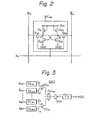
- Fig. 2 illustrates a memory cell for example MC oo , used in the circuit of Fig. 1.
- the memory cell MC oo comprises load transistors Q 21 , Q 22 and driver transistors Q 23 , Q 24 which compose a flip-flop, and gate transistors Q 25 , Q 26 which are turned on and .off by the output signal, i.e., decoded address signal X o from the X address decoder XD 0 .
- the gate transistors Q 25 and Q 26 are turned on due to the supply of a decoded address signal X o of high potential level, and transfer of information between the bit lines B o , B o and the flip-flop of the memory cell MC oo is effected.
- Fig. 3 illustrates a gate signal generator which produces a delayed gate signal WDD and which comprises a detector circuit DXD consisting of trigger pulse generators TG 01 , TG 02 , ..., TG M1 , TG M2 , OR gates OG o , ..., OG M , OG oo and an inverter INV, and, a delay circuit TD.
- Each of the trigger pulse generators TG 01 through TG M2 detects potential change, i.e.
- OR gates OG 0 through OG M and an OR gate OG oo effect the logical "or" operation of the trigger pulses To, T' o , ..., T M , T' M .
- the inverter INV inverts an output signal from the OR gate OG oo and produces a gate. signal T.
- a delay circuit TD delays the gate signal T for a predetermined time period and produces the delayed gate signal WDD, which was mentioned before.
- the delay time of the delay circuit TD is a time in which the output signal X o , ..., X N-1 or X N respectively reaches from the X address decoder XD 0 , ..., XD N-1 , or XD N to the farthest end of the word line W 0 , ..., W N-1 or W N , i.e., a portion of the word line to which the memory cell MC 0N , ..., MC N-1 N or MC NN is connected in the embodiment of Fig. 1.
- the delay circuit TD can be constructed by using a dummy word line which has approximately the same length as that of each of the word lines W o through W N and which is disposed parallel to the word lines W o through W N .
- each of the trigger pulse generators TG 01 , through TG M2 can be constructed by using, for example, a differentiation circuit and a wave shaping circuit.
- a part of the address signals A o , A o , ..., A M , A M are applied to the X address decoders XD 0 through XD N and a part of the address signals are applied to Y address decoders, which are not shown in the drawings.
- the output X o from the X address decoder XD 0 turns to high and the output Y o from the Y address decoder turns to high.
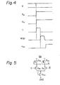
- At least two of the address signals A o , A o , ..., AM, A M change their potential level, as illustrated by A of Fig. 4.
- This change of the potential level may be of a potential rise or a potential fall.
- the detector circuit DXD In response to the change of the potential level of at least one address signal, the detector circuit DXD generates a gate signal T as illustrated in Fig. 4.
- the delay circuit TD delays the gate signal T and produces the delayed gate signal WDD, as illustrated in Fig. 4.
- the delayed gate signal WDD is applied to the gate electrodes of the transistors Q 5 and Q 6 of the latch circuits RA 0 through RA N .
- the potential of all portions of the selected word line W o has already risen to a high level. Therefore, the information from the memory cell MC oo , which is disposed in the nearest position from the X address decoder XD 0 in Fig. 1, has already been read out to the bit line pair B o , B o . That is, the potentials of the point A and the point B in the memory cell MC oo has already been transferred to the bit lines B o and B o respectively.
- the gate transistors Q 5 and Q 6 are turned on by the delayed gate signal WDD and the information of the memory cell MC oo , i.e. the potentials of the point A and the point B of the memory cell MC oo , is input to the latch circuit RA o through the gate transistors Q 5 and Q 6 .
- the delayed gate signal WDD is applied to the gate transistors Q 5 and Q 6
- the delayed Y decoder signal Y 0D is applied to the gate electrodes of the switching transistor Q 7 and the load transistors Q 1 and Q 2 of the latch circuit RA o , so that the latch circuit RA o is activated, due to the supply of an operating voltage.
- the latch circuit RA o is set to a condition determined by the input potentials, i.e. the potentials of the bit lines B o and B o , so that the transferring of information to the latch circuit RA o is effected.
- the input potentials i.e. the potentials of the bit lines B o and B o
- stray capacitances existing between the input circuit portion of the latch circuit RA 0 and the ground are charged by the potentials of the bit lines B o and B o . Therefore, even if the delayed Y decoder signal Y oo is applied to the latch circuit RA 0 a short time after the delayed gate signal WDD has changed from high potential to low potential, as illustrated in Fig.
- the latch circuit RA 0 it is possible to set the latch circuit RA 0 to a condition determined by the potentials of the bit lines B o and B o . It should be noted that the delayed gate signal WDD and the delayed Y decoder signal Y 0D are needed in order to prevent the destruction of data in the memory cell MC oo .
- the memory cell MC oo having a small drive capacity is written-in by the potentials of the bit lines B o and B o which are determined by the condition of the latch circuit RA 0 at the time the memory cell MC oo is selected.
- Fig. 5 illustrates an example of a sense amplifier SA which is used in the memory device of Fig. 1.
- the sense amplifier SA comprises a pair of transistors Q 50 and Q 51 composing a differential amplifier, a pair of load transistors Q 12 and Q 53 , and a transistor Q 54 composing a constant current source.
- the gate electrodes of the transistors Q 50 and Q 51 are respectively connected to the output terminals of the latch circuits RA 0 through RA N through data bus lines which are not shown in the drawings. Therefore, the output signals D and D of the latch circuit, for example, RA 0 are respectively applied to the gate electrodes of the transistors Q 50 and Q 51 , and amplified by the sense amplifier SA.
- the sense amplifier SA provides output signals O and O as the read-out signals from the memory device.
- the data bus lines and the sense amplifier are driven by the latch circuits, whose driver transistors are big in size, so as to obtain a large drive capacity so that it is possible to increase the read-out speed and to improve the reliability of the read-out data of the static type RAM device. Therefore, it is not necessary to use memory cells having big sizes and a latch circuit is provided for every column, so that the integration degree of the RAM device is not so much decreased.
Landscapes
- Engineering & Computer Science (AREA)
- Microelectronics & Electronic Packaging (AREA)
- Computer Hardware Design (AREA)
- Static Random-Access Memory (AREA)
- Dram (AREA)
Claims (7)
Applications Claiming Priority (2)
| Application Number | Priority Date | Filing Date | Title |
|---|---|---|---|
| JP154578/79 | 1979-11-29 | ||
| JP54154578A JPS59915B2 (ja) | 1979-11-29 | 1979-11-29 | メモリ回路 |
Publications (3)
| Publication Number | Publication Date |
|---|---|
| EP0031995A2 EP0031995A2 (de) | 1981-07-15 |
| EP0031995A3 EP0031995A3 (en) | 1982-11-17 |
| EP0031995B1 true EP0031995B1 (de) | 1986-02-26 |
Family
ID=15587274
Family Applications (1)
| Application Number | Title | Priority Date | Filing Date |
|---|---|---|---|
| EP80304189A Expired EP0031995B1 (de) | 1979-11-29 | 1980-11-21 | Halbleiterspeicheranordnung mit matrixartig angeordneten statischen Speicherzellen |
Country Status (6)
| Country | Link |
|---|---|
| US (1) | US4400800A (de) |
| EP (1) | EP0031995B1 (de) |
| JP (1) | JPS59915B2 (de) |
| CA (1) | CA1174762A (de) |
| DE (1) | DE3071458D1 (de) |
| IE (1) | IE51438B1 (de) |
Families Citing this family (9)
| Publication number | Priority date | Publication date | Assignee | Title |
|---|---|---|---|---|
| JPS5838873B2 (ja) * | 1980-10-15 | 1983-08-25 | 富士通株式会社 | センス回路 |
| JPS57141097A (en) * | 1981-02-25 | 1982-09-01 | Toshiba Corp | Storage circuit |
| DE3582376D1 (de) * | 1984-08-03 | 1991-05-08 | Toshiba Kawasaki Kk | Halbleiterspeicheranordnung. |
| US4636991A (en) * | 1985-08-16 | 1987-01-13 | Motorola, Inc. | Summation of address transition signals |
| JPH0831275B2 (ja) * | 1986-09-09 | 1996-03-27 | 日本電気株式会社 | メモリ回路 |
| JPH01174563U (de) * | 1988-05-30 | 1989-12-12 | ||
| US5023842A (en) * | 1988-07-11 | 1991-06-11 | Kabushiki Kaisha Toshiba | Semiconductor memory having improved sense amplifiers |
| DE4107420C2 (de) * | 1991-03-08 | 2002-08-14 | Zentr Mikroelekt Dresden Gmbh | Schreib-Lese-Schaltung für einen statischen RAM |
| US7102946B2 (en) * | 2005-02-09 | 2006-09-05 | International Business Machines Corporation | Local bit select circuit with slow read recovery scheme |
Family Cites Families (3)
| Publication number | Priority date | Publication date | Assignee | Title |
|---|---|---|---|---|
| US3879621A (en) * | 1973-04-18 | 1975-04-22 | Ibm | Sense amplifier |
| JPS538528A (en) * | 1976-07-12 | 1978-01-26 | Nec Corp | Memory circuit |
| JPS5472641A (en) * | 1977-11-21 | 1979-06-11 | Toshiba Corp | Voltage detection circuit |
-
1979
- 1979-11-29 JP JP54154578A patent/JPS59915B2/ja not_active Expired
-
1980
- 1980-11-18 CA CA000364903A patent/CA1174762A/en not_active Expired
- 1980-11-21 DE DE8080304189T patent/DE3071458D1/de not_active Expired
- 1980-11-21 EP EP80304189A patent/EP0031995B1/de not_active Expired
- 1980-11-25 IE IE2439/80A patent/IE51438B1/en not_active IP Right Cessation
- 1980-11-26 US US06/210,663 patent/US4400800A/en not_active Expired - Lifetime
Also Published As
| Publication number | Publication date |
|---|---|
| JPS59915B2 (ja) | 1984-01-09 |
| US4400800A (en) | 1983-08-23 |
| EP0031995A2 (de) | 1981-07-15 |
| CA1174762A (en) | 1984-09-18 |
| JPS5677982A (en) | 1981-06-26 |
| EP0031995A3 (en) | 1982-11-17 |
| IE51438B1 (en) | 1986-12-24 |
| IE802439L (en) | 1981-05-29 |
| DE3071458D1 (en) | 1986-04-03 |
Similar Documents
| Publication | Publication Date | Title |
|---|---|---|
| US4161040A (en) | Data-in amplifier for an MISFET memory device having a clamped output except during the write operation | |
| US4528646A (en) | Semiconductor memory with selectively enabled precharge and sense amplifier circuits | |
| US3906464A (en) | External data control preset system for inverting cell random access memory | |
| US4766572A (en) | Semiconductor memory having a bypassable data output latch | |
| EP0023510B1 (de) | Speicher aufbau zum reduzieren des scheitelstroms | |
| US4099265A (en) | Sense line balance circuit for static random access memory | |
| EP0405055B1 (de) | Vorlade-Architektur von integrierten Speichern | |
| US4322825A (en) | Flexible hidden refresh memory circuit | |
| EP0316902B1 (de) | Halbleiterspeicherschaltung mit einem verbesserten Rückschreibschema | |
| US4110840A (en) | Sense line charging system for random access memory | |
| KR19980069694A (ko) | 낮은 전원공급전압에서 고속동작을 하는 반도체 메모리장치 | |
| EP0194939B1 (de) | Halbleiterspeicheranordnung | |
| EP0098164B1 (de) | Statische Halbleiterspeicheranordnung | |
| US5148400A (en) | Semiconductor memory circuit having an improved restoring control circuit | |
| US4400800A (en) | Semiconductor RAM device | |
| EP0058051B1 (de) | Statische Halbleiterspeicheranordnung | |
| US6154404A (en) | Integrated circuit memory devices having sense amplifier driver circuits therein that improve writing efficiency | |
| US4680734A (en) | Semiconductor memory device | |
| EP0050037B1 (de) | Halbleiterspeicheranordnung | |
| US4500974A (en) | Memory circuit | |
| EP0115140B1 (de) | Dekodierschaltung | |
| US4653027A (en) | Semiconductor memory device | |
| US4823322A (en) | Dynamic random access memory device having an improved timing arrangement | |
| US4554469A (en) | Static bootstrap semiconductor drive circuit | |
| US4514831A (en) | Static-type semiconductor memory device |
Legal Events
| Date | Code | Title | Description |
|---|---|---|---|
| PUAI | Public reference made under article 153(3) epc to a published international application that has entered the european phase |
Free format text: ORIGINAL CODE: 0009012 |
|
| 17P | Request for examination filed |
Effective date: 19801202 |
|
| AK | Designated contracting states |
Designated state(s): DE FR GB NL |
|
| PUAL | Search report despatched |
Free format text: ORIGINAL CODE: 0009013 |
|
| AK | Designated contracting states |
Designated state(s): DE FR GB NL |
|
| GRAA | (expected) grant |
Free format text: ORIGINAL CODE: 0009210 |
|
| AK | Designated contracting states |
Designated state(s): DE FR GB NL |
|
| ET | Fr: translation filed | ||
| REF | Corresponds to: |
Ref document number: 3071458 Country of ref document: DE Date of ref document: 19860403 |
|
| PLBE | No opposition filed within time limit |
Free format text: ORIGINAL CODE: 0009261 |
|
| STAA | Information on the status of an ep patent application or granted ep patent |
Free format text: STATUS: NO OPPOSITION FILED WITHIN TIME LIMIT |
|
| 26N | No opposition filed | ||
| PGFP | Annual fee paid to national office [announced via postgrant information from national office to epo] |
Ref country code: FR Payment date: 19951109 Year of fee payment: 16 |
|
| PGFP | Annual fee paid to national office [announced via postgrant information from national office to epo] |
Ref country code: GB Payment date: 19951113 Year of fee payment: 16 |
|
| PGFP | Annual fee paid to national office [announced via postgrant information from national office to epo] |
Ref country code: DE Payment date: 19951128 Year of fee payment: 16 |
|
| PGFP | Annual fee paid to national office [announced via postgrant information from national office to epo] |
Ref country code: NL Payment date: 19951129 Year of fee payment: 16 |
|
| PG25 | Lapsed in a contracting state [announced via postgrant information from national office to epo] |
Ref country code: GB Effective date: 19961121 |
|
| PG25 | Lapsed in a contracting state [announced via postgrant information from national office to epo] |
Ref country code: NL Effective date: 19970601 |
|
| GBPC | Gb: european patent ceased through non-payment of renewal fee |
Effective date: 19961121 |
|
| PG25 | Lapsed in a contracting state [announced via postgrant information from national office to epo] |
Ref country code: FR Effective date: 19970731 |
|
| NLV4 | Nl: lapsed or anulled due to non-payment of the annual fee |
Effective date: 19970601 |
|
| PG25 | Lapsed in a contracting state [announced via postgrant information from national office to epo] |
Ref country code: DE Effective date: 19970801 |
|
| REG | Reference to a national code |
Ref country code: FR Ref legal event code: ST |