EP0034018A2 - Appareil de conditionnement de puissance - Google Patents
Appareil de conditionnement de puissance Download PDFInfo
- Publication number
- EP0034018A2 EP0034018A2 EP81300379A EP81300379A EP0034018A2 EP 0034018 A2 EP0034018 A2 EP 0034018A2 EP 81300379 A EP81300379 A EP 81300379A EP 81300379 A EP81300379 A EP 81300379A EP 0034018 A2 EP0034018 A2 EP 0034018A2
- Authority
- EP
- European Patent Office
- Prior art keywords
- output
- waveshape
- reactor
- load
- input
- Prior art date
- Legal status (The legal status is an assumption and is not a legal conclusion. Google has not performed a legal analysis and makes no representation as to the accuracy of the status listed.)
- Granted
Links
- 230000003750 conditioning effect Effects 0.000 title claims abstract description 6
- 239000003990 capacitor Substances 0.000 claims abstract description 35
- 238000004804 winding Methods 0.000 claims abstract description 17
- 230000001052 transient effect Effects 0.000 claims description 16
- 230000001105 regulatory effect Effects 0.000 claims description 15
- 230000000694 effects Effects 0.000 claims description 13
- 238000010168 coupling process Methods 0.000 claims description 10
- 230000008878 coupling Effects 0.000 claims description 9
- 238000005859 coupling reaction Methods 0.000 claims description 9
- 230000007935 neutral effect Effects 0.000 claims description 7
- 230000003534 oscillatory effect Effects 0.000 claims description 5
- 238000009738 saturating Methods 0.000 claims description 5
- 230000003467 diminishing effect Effects 0.000 claims description 4
- 230000004044 response Effects 0.000 claims description 3
- 230000002194 synthesizing effect Effects 0.000 abstract description 15
- 238000000034 method Methods 0.000 abstract description 10
- 230000035939 shock Effects 0.000 description 13
- 230000005291 magnetic effect Effects 0.000 description 9
- 230000015572 biosynthetic process Effects 0.000 description 7
- 238000013461 design Methods 0.000 description 7
- 230000004075 alteration Effects 0.000 description 6
- 238000012937 correction Methods 0.000 description 6
- 210000002414 leg Anatomy 0.000 description 4
- 230000004907 flux Effects 0.000 description 3
- 238000009434 installation Methods 0.000 description 3
- 238000012546 transfer Methods 0.000 description 3
- XEEYBQQBJWHFJM-UHFFFAOYSA-N Iron Chemical compound [Fe] XEEYBQQBJWHFJM-UHFFFAOYSA-N 0.000 description 2
- 229910000831 Steel Inorganic materials 0.000 description 2
- 238000013459 approach Methods 0.000 description 2
- 230000008859 change Effects 0.000 description 2
- 238000010586 diagram Methods 0.000 description 2
- 230000001939 inductive effect Effects 0.000 description 2
- 238000002955 isolation Methods 0.000 description 2
- 230000005415 magnetization Effects 0.000 description 2
- 238000009877 rendering Methods 0.000 description 2
- 238000012163 sequencing technique Methods 0.000 description 2
- 239000010959 steel Substances 0.000 description 2
- 238000003786 synthesis reaction Methods 0.000 description 2
- BVGSSXDMHDNNIF-UHFFFAOYSA-N (4-oxo-2,3-dihydro-1h-cyclopenta[c]chromen-7-yl) 3-chloro-4-[2-[(2-methylpropan-2-yl)oxycarbonylamino]acetyl]oxybenzoate Chemical compound C1=C(Cl)C(OC(=O)CNC(=O)OC(C)(C)C)=CC=C1C(=O)OC1=CC=C(C2=C(CCC2)C(=O)O2)C2=C1 BVGSSXDMHDNNIF-UHFFFAOYSA-N 0.000 description 1
- RYGMFSIKBFXOCR-UHFFFAOYSA-N Copper Chemical compound [Cu] RYGMFSIKBFXOCR-UHFFFAOYSA-N 0.000 description 1
- 238000010521 absorption reaction Methods 0.000 description 1
- 230000004308 accommodation Effects 0.000 description 1
- 230000009471 action Effects 0.000 description 1
- 238000004883 computer application Methods 0.000 description 1
- 229910052802 copper Inorganic materials 0.000 description 1
- 239000010949 copper Substances 0.000 description 1
- 125000004122 cyclic group Chemical group 0.000 description 1
- 230000007812 deficiency Effects 0.000 description 1
- 238000001514 detection method Methods 0.000 description 1
- 230000002542 deteriorative effect Effects 0.000 description 1
- 238000005516 engineering process Methods 0.000 description 1
- 210000003414 extremity Anatomy 0.000 description 1
- 238000001914 filtration Methods 0.000 description 1
- 238000011835 investigation Methods 0.000 description 1
- 229910052742 iron Inorganic materials 0.000 description 1
- 210000003127 knee Anatomy 0.000 description 1
- 230000003472 neutralizing effect Effects 0.000 description 1
- 230000010355 oscillation Effects 0.000 description 1
- 230000002265 prevention Effects 0.000 description 1
- 238000012545 processing Methods 0.000 description 1
- 230000003068 static effect Effects 0.000 description 1
Images


Classifications
-
- G—PHYSICS
- G05—CONTROLLING; REGULATING
- G05F—SYSTEMS FOR REGULATING ELECTRIC OR MAGNETIC VARIABLES
- G05F3/00—Non-retroactive systems for regulating electric variables by using an uncontrolled element, or an uncontrolled combination of elements, such element or such combination having self-regulating properties
- G05F3/02—Regulating voltage or current
- G05F3/04—Regulating voltage or current wherein the variable is AC
- G05F3/06—Regulating voltage or current wherein the variable is AC using combinations of saturated and unsaturated inductive devices, e.g. combined with resonant circuit
Definitions
- Line power now available from utility organizations has been observed to be deteriorating in quality to the extent that, in numerous instances, it has become unacceptable for direct application to computer systems.
- Vagaries in line power stem from many causes but are categorized principally as line noise and out of specification voltage.
- Line noise may develop from a variety of perturbations, for example spikes may develop due to short circuits along the distribution lines, radio frequency interference, lightning or power factor corrections manifested as oscillatory ringing transients. These transients generally are in a range of 200%-400% of the normal voltage envelope. Under-voltage or over-voltage phenomena generally occur in conjunction with regulator activity and load changing on the power line.
- these ferroresonant regulators comprise a non-linear saturable transformer in parallel with a capacitor which is supplied from a source through a linear reactor.
- the saturable transformer and the capacitor form a ferroresonant circuit wherein the inductive components operate beyond the knee of a conventional magnetization curve.
- These devices have been seen to hold considerable promise, inasmuch as they are inherently simple, requiring very few components. For example, it is the inherent nature of the ferroresonant transformer to handle all regulating, harmonic neutralizing and current-limiting functions thus permitting the noted simplification.
- the approach eliminates the need for feedback loops which, as noted above, are found in line voltage regulators.
- An absence of such loops provides for very reliable and stable current limit and regulation that are inherent to the device and not subject to change or alteration due to component failures.
- This lack of closed-loop feedback circuits makes the ferroresonant device quite insensitive to non-linear or pulse loads. Because the waveshape is completely recreated, transients and high speed phenomena cannot penetrate the ferroresonant devices.
- ferroresonant devices While ferroresonant devices have found use in inverter applications and the Like, their use as a line voltage regulator, per se, in conjunction with computer and other installations has not found favor. This principally is due to their statistically unreliable performance on unbalanced three phase loadss; their tendency toward instability under certain three phase loading conditions; and their inability to provide high currents sometimes required in starting loads. Earlier designs also have tended to be unstable at light loads due to low input choke impedance. Three phase ferroresonant regulators have been observed to exhibit instability in developing a proper sinewave output. When instability results in a loss of a proper sinewave output for computer utilization, the computers necessarily are shut down.
- the devices hold promise of finding widespread use as a power conditioning system.
- the single phase ferroresonant regulators could be made operable under all three phase loading conditions, if three phase ferroresonant regulators could be designed such that their outputs do not fall into non-sinewave patterns, the ferroresonant type regulators would exhibit a highly desirable voltage regulation technique.
- the design of the ferroresonant regulators to avoid instability is one which is heueristic in nature and achieving a satisfactory result is an evasive endeavor.
- a more recent aspect of the power requirements of computer facilities is concerned with the accommodation of high start-up surge currents in computer components. It is desirable that line power be regulated to provide a proper sinewave input to the computer facility as well as to provide over-voltage and under-voltage regulation. However, for the transient period of start-up, there is required a capability for delivering as much surge current as possible to the computer components. For example, a typical motor utilized in computer devices will draw three amps current under steady state condition while it may draw as much as 20 amps for a matter of seconds while it is starting up and developing proper speed. A traditional weakness of ferroresonant transformers has been that they are unable to supply such start-up surges. Further, inverter devices utilizing ferroresonant techniques are designed specifically not to pass high currents and to transfer to alternate power in the event of a call for surge currents. Summary
- distorted output waveshapes which for illustration is desired to be sinusoidal, of the synthesizer networks have been found to contain significant second harmonics, a phenomena heretofore seldomly encountered.
- a third harmonic also is detected in certain of the distorted output waveshapes along with higher order harmonics in lesser amount.
- the distorted output waveshapes develop from an energy related improper association of components within the synthesizing networks which have been found to be generated in consequence of a form of shock occasioned from a variety of transient electrical occurrences. For example, such shocks may occur over a statistically unacceptable number of instances at start-up, during load dumping, during load shedding and other such occurrences.
- series tuned trap circuits coupled with the synthesizer network at a location effecting the output waveshape to substantially reduce the tendency thereof to evolve harmonics above fundamental, a highly stable, properly configured sinewave output is assured.
- the apparatus to be described accommodates initial start-up current surges, permitting its utilization with modern computer facilities requiring such surge inputs.
- the system is capable of carrying a high current under overload conditions.
- the line power is tightly coupled to the load, the synthesizing network of the system essentially being overridden.
- the system reverts to its proper waveshape synthesizing performance, in consequence of the utilization of the above-described series tuned trap arrangement.
- the present invention provides in one aspect apparatus for use with an a.c. source of variable voltage level and waveshape, and having given frequency for providing a regulated a.c. output to a load, comprising:
- an input choke configured having a non-linear response characteristic for effecting a substantial impedance at levels of said load extending from low values to full load conditions and effecting a diminishing impedance to said a,c. source for overload conditions to effect the conveyance of transient load start-up surge currents.
- the synthesizer network oscillatory saturation performance is effectively overridden during the conveyance of such surge currents.
- the input chokes are formed incorporating a selectively gapped center leg.
- the regulating apparatus is particularly suited by virtue of its reliability and quality of regulation for use in conjunction with computer facilities.
- Such facilities are centrally located within a building and, over the recent past, have been formed of components which are somewhat movable so as to afford a flexibility of computer system design.
- regulators fabricated in accordance with the invention preferably are structured so as to provide a modularity or mobility such that they may be maneuvered within the computer environment to supply regulated power for any of a variety of computer component configurations.
- a modular form of power regulator cabinet is represented generally at 10.
- the forward control panel of the power management assembly represented at 10 is removed such that the shelves upon which reactors and the like are positioned may be schematically portrayed.
- a bank of three regulating transformers, TXI, TX2 and TX3 are shown mounted upon an upper shelf 12, such mounting, respectively, being provided through the use of spring mounted supports 14-19.
- an intermediate shelf 20 supports saturable reactors TX4, TX5 and TX6 through spring mounted supports 22-27.
- the bottom shelf 28 of assembly 10 supports a combination of input chokes TX7, TX8 and TX9 as well as a neutral deriving or grounding transformer, not shown, TX10.
- Assembly 10 also includes a bank of delta connected capacitors represented generally at 30 and a series of traps at shelf 20 which include capacitors and reactors represented generally at 32.
- FIG. 2 a schematic diagram showing all the components represented within the assembly 10 is shown.
- the drawing reveals an input side of the reuglator apparatus at 40 having three input lines 42-44 which are connectible to a conventional utility derived power supply and which represent the line input to the regulating features.
- Lines 42-44 extend, in turn, to input chokes TX7, TX8 and TX9.
- These input chokes are configured by gapping techniques and the like to exhibit a variable impedance to line input.
- Input chokes TX7-TX9 perform as a buffer at the source of power represented by the line source 42-44 which has a unique sine waveshape and a unique voltage associated with it.
- the input chokes transfer the energy of that power source into a sine wave synthesizer represented generally at 50 without transferring thereinto the wave shape associated with incoming lines 42-44 or the voltage characteristics thereof.
- chokes TX7-TX9 act as a very spongy connection between the power line input and the synthesizer 50 as to isolate these two sources from each other.
- Synthesizer 50 requires, from the line source, energy within a usable band of voltage and having a frequency reference (60 0 Hz), the synthesizer 50 following the frequency at the line power source.
- the synthesizer network 50 is comprised of six saturable reactors TXI-TX6 which operate in concert with a capacitor bank represented generally, as in Fig. 1, at 30.
- the saturating reactors have the ability to change their impedance very rapidly from an open circuit to a short circuit condition as saturation is carried out.
- These six reactors saturate in a sequence such that when one saturates, it drives another out of saturation.
- the saturation frequency rotates at line frequency, a unique pulse or pulses may be evolved from each reactor for every one- half cycle. The pulse height depends upon the characteristic of the reactor, i.e.
- saturable reactors TX4, TX5, and TX6 are coupled with respective lines 52-54 and are configured as saturating reactors with a single secondary or choke configuration. These reactors are coupled through respective lines 56-58 to reactors TXI, TX2 and TX3.
- reactors are shown wired as transformers and are interconnected in zig-zag fashion, a technique conventionally used in forming grounding transformers as are used in utility functions to achieve a neutral output from three wires.
- Reactors TXl-TX3 additionally are shown to be coupled in series with reactors TX4-TX6.
- Capacitor bank 30 incorporating a capacitor formation represented at 60 in line 62, capacitor formation 64 in line 67 and capacitor formation 66 in line 68 are connected in conventional delta configuration for connection with the saturable reactors. These capacitors serve as storage elements which maintain the lower six saturable reactors in oscillation. To achieve the sine wave form of Fig. 2A, the latter saturable reactors must saturate and ring with the capacitors within capacitor bank 30.
- the output of input choke TX9 is present at line 76 which is coupled in series with primary winding TX6' which is operatively associated with reactor TX6 and with TX3' which is operatively associated in primary winding fashion with reactor TX3.
- Windings TXI'-TX3' are interconnected in the earlier described zig-zag configuration.
- Faraday shields 78-80 are shown associated with the cores of respective windings TX4'-TX6', while similar Faraday shields 82-84 are shown associated with the cores of primary windings TXl'-TX3'. These Faraday shields are shown coupled to a conventional ground or neutral position represented by connection 85.
- the Faraday shields extend between primary and secondary windings and are connected to ground to lower interwinding capacitance and thus prevent the transfer of common mode line noise therebetween. It is important to note that, through the use of magnetic coupling of energy from the line input region 40 to the synthesizing components 50, a series coupling is evolved. Such a series coupling improves the performance of the overall device inasmuch as it prevents the passthrough of common mode noise. Further, the coupling technique is found helpful in stepping up or stepping down voltage and avoids dangerous voltage excursions in the event of catastrophic failure occasioned through broken wires or the like. Where such breakage occurs, the energy source is removed from the system to avoid damage.
- Synthesizing network 50 when operationally combined with the input chokes TX7-TX9 and the capacitor bank 30, serves to generate a three phase waveshape, however, the combination does not serve to generate a neutral or reference output. Consequently, a grounding transformer represented at 86 having input lines 88-90 coupled with respective lines 52-54 of synthesizer network 50 is provided. Grounding transformer 86 is provided combining three coil structures identified at TX10 which combine with a single three phase core to generate a neutral wire represented at 92. Note, that the coils of transformer 86 are interconnected in the earlier described zig-zag fashion. Neutral output is provided at output terminal 92 which serves in conjunction with output terminals 94-96 of the synthesizing network 50 which are coupled, respectively, with lines 52-54.
- the regulating system When considered statically, the regulating system thus far described is one providing highly consistent sine wave output immune from the vagaries which may be developed at the line input 40.
- the sine wave formation developed exhibits only eleventh harmonic characteristics above and beyond the fundamental.
- This sinewave generating condition represents a conservation of. energy, examination of the power characteristic of the system showing that it is absorbing the least energy when evolving a proper sinewave.
- the sinewave configuration and condition of least energy absorption has been observed to be one which essentially always is present as the system operates under heavy loads.
- the technique of regulation is one which is statistically unreliable due, it has been discovered, to its susceptibility to "shocks" which may be occasioned from numerous conditions and which result in non-sinusoidal waveshapes which will persist unless corrected.
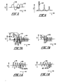
- Figs. 3 and 4 Two such waveshapes are shown in Figs. 3 and 4, that shown in Fig. 3 at 102 representing distortion of even harmonics, while that shown at 104 in Fig. 4 representing a combination of odd harmonics.
- These waveshapes represent an improper sequencing of the pulses evolved from the synthesizing network 50 as well as an operation of that network not at its lowest available energy utilization level.
- the triggering or shocking of synthesizer network 50 developing these aberrations has been discovered to emanate from any of a variety of transient causes. It may occur at turn on; through the application of a short circuit at some point following the release thereof; internal failures, for example arcing connections, as well as the turning on of a transformer at some position within the load, which transformer may retain a heavy magnetizing current.
- a typical a.c. wave is shown at 106 as introduced to a load transformer. If the transformer is turned off, for example at a time represented at 108, a positive half cycle of magnetization will remain in its core.
- the initial peaks shown at waveshape 110 are relatively large, ranging from 300-400 amps.
- the result with respect to regulation of the input to the load is one wherein a d.c. level is drawn from the synthesizing source. This represents a shock which can evolve aberrational output waveshapes as described earlier in connection with Figs. 3 and Fig. 4 on a statistical basis which is unacceptable.
- any load device will draw some form of d.c. surge at start up, depending upon the state of its inductive elements at turn off.
- a typical output voltage representation of the synthesizing network 50 is shown at a point of turn on. Note, that the voltage peaks or excursions extend to about 160% of the normal operational envelope during start up without correction. This condition can represent a shock situation as above discussed.
- the initial hunting interval is represented in Fig. 7A at 112, while a normal voltage output for the synthesizing network is represented adjacent thereto at 114.
- FIG. 8A Another condition which may arise leading to a "shock" phenomena occurs upon the picking up of a load.
- the normal output of the synthesizer network is represented at waveform 116.
- an excursion representing 70%-80% of normal waveshape envelope may be witnessed. This has been discovered to be a sufficient phenomena to evolve a shock condition leading to a continuous aberration of the output waveshape of synthesizer network 50.
- Still another transient condition which may be encountered, typically in the operation of computer systems is that of dumping a load.
- a conventional output waveshape is represented at curve portion 120, while the transient phenomena associated with load dumping is represented by excursion portion 122 of the waveform. This excursion may represent a 60% excursion of the normal peak envelope. The occurrence of this transient phenomenon will cause the synthesizing network 50 to temporarily lapse into a non-sinusoidal wave output.
- the correction to the system and apparatus which ameliorates the above-noted transient phenomena such that a "shock" condition causing the ferroresonant system to lose its proper sequencing capability is effectively avoided is represented by the network of traps shown generally at 32.
- These traps include six reactors and associated capacitors configured in the form of tuned circuits that are connected across the output of synthesizer network 50.
- One combination of three of these series tuned traps is represented generally at 130 as including a first series resonant circuit formed of capacitor 132 and reactor 134.
- a second series resonant circuit of combination 130 is represented by capacitor 136 and reactor 138, while a third series resonant circuit or trap is represented by capacitor 140 and reactor 142.
- Trap combination 130 is connected in delta configuration and the capacitive and reactive components of each circuit therein are selected to resonate at the third harmonic.
- Connection of the delta configuration 130 across the output of the system is by lines 144 and 145 coupled, respectively, to lines 52 and 54, and by lines 146 and 147, the latter being coupled to line 53.
- a second trap combination is represented generally at 150 and includes an initial series resonant circuit including capacitor 152 and reactor 154.
- a second series resonant circuit is shown comprising reactor 156 in operational combination with capacitor 158, while a third series resonant circuit within the combination is represented by capacitor 160 operating in association with reactor 162.
- the series tuned traps of combination 150 also are coupled in delta configuration and that the components thereof are selected so as to be tuned to the second harmonic. Connection of trap combination 150 with lines 52 and 54 is through respective lines 144 and 145, while connection thereof to line 53 is from line 147.
- trap combinations 130 and 150 will remain passive within the system, an ideal sinewave output being generated by network 50 which is immune from line input variations of considerable magnitude.
- the trap combinations 130 and 150 will short out the harmonic energy thereof, such energy having been discovered to be a principal component of the transient phenomena.
- the aberrational output waveforms of network 50 always will include significant second and/or third harmonic components. This phenomenon obtains for every one of the non-sinewave modes which the system can revert to.
- Fig. 3 represents a condition wherein only even harmonics are involved, including the second harmonic.
- this second harmonic investigators have considered the presence thereof to be highly unusual, representing an unsymmetrical waveform not usually generated with conventional devices.
- Fig. 4 shows an output waveshape aberration incorporating only odd harmonics.
- the trap combinations as at 130 and 150 serve to force the energy representing unwanted harmonics back to the fundamental as a form of energy reflection.
- the positioning of the series tuned trap with the synthesizer network 50 should be at a location affecting the output waveshape thereof with respect to harmonics above fundamental and below the eleventh harmonic, the latter harmonic occurring in conjunction with the pulse formation of the sinusoidal waveshape. Consequently, the traps can be positioned at any location wherein the output waveshape is witnessed, i.e. any position where they can affect the synthesized or created waveshape, for example the position functionally within the circuit beyond the output of input chokes TX7-TX9.
- other trap configurations may be provided other than the preferred arrangement shown at 32.
- the function may be carried out utilizing a single resonant trap circuit tuned for operation at an intermediate point between the second and third harmonic.
- Other trap combination couplings also may be utilized, for example open delta, wye or simple phase line-to-line.
- Fig. 7B the result of utilizing a trap network as at 32 is shown in connection with a typical waveshape 170 encountered during turn-on phenomena. Note, that the excursion at turn-on, of the peaks is limited to about 30% of the normal operational waveshape envelope as opposed to the 60% valuation described in connection with Fig. 7A. Similarly, looking to Fig. 8B, the effect upon waveshape 172 upon the occurrence of a load pickup phenomenon is represented. Note that the voltage excursion is limited to 80%-95% of the normal operational peak envelope thereof. Further, looking to Fig. 9B, waveshape 174 shows the effect of trap network 32 during load dumping.
- the voltage excursion during load dumping is limited to about 30% of the normal waveshape envelope. All of these corrections have been found sufficient to eliminate the "shock" effect to the extent that aberrational output waveshapes are effectively eliminated.
- the more recent designs of computer facilities have called for equipment necessarily requiring significant surge currents at start-up.
- regulator systems are not designed to accommodate for such surge current requirements, inverter systems typically switching to stand-by power implements upon the initial detection of a surge current.
- acapability is provided for supplying those surge currents to the load by closely coupling the line input power source with the load during that transient interval requiring a surge-categorized input.
- the input chokes TX7-TX9 are configured having a highly non-linear characteristic. This characteristic is arranged such that for conditions extending from relatively light or low loads through full design load, a relatively high impedance is effected. Generally, this is carried out by selective gapping techniques.
- the input chokes are designed so as to lower the impedance exhibited thereby and permit the conveyance of surge current from the source to the load.
- a very close coupling of the input chokes with the load is achieved by the selective non-linearity of the former.
- the conventional sinewave output of synthesis network 50 becomes passive to permit surge condition coupling.
- high currents are evolved and the output voltage of the system drops.
- the ferroresonance achieved at network 50 essentially is stopped.
- the voltage available is lower than the voltage at which network 50 operates in a ferroresonant attitude.
- the system carries on in a normal sinewave synthesizing mode as is required for normal computer facility performance. Because of the performance of resonant trap network 32, however, the transient "shock" effect which otherwise would drive the synthesizing components to produce an unacceptable waveform are avoided through short circuiting of the earlier-discussed harmonics.
- Fig. 10 a series of characteristic curves for input chokes suited for the instant purpose are revealed at 180, 182, and 184.
- the curves in the figure plot impedance in ohms, as exhibited by the input chokes, with respect to voltage across the chokes, which voltage is directly related to load value.
- the curves 180, 182 and 184 are derived from triple gap core input chokes having the labeled number of turns. Typically, a full load condition will be represented by a voltage of about 140 volts. Looking to the impedance range for each of the curves within that voltage related load valuation, it may be seen that the impedance characteristic, while diminishing, remains relatively high for loads ranging from minimal to full load.
- the chokes exhibit an impedance characteristic wherein the impedance exhibited thereby diminishes significantly. This permits the surge coupling capability of the apparatus of the invention as described hereinabove.
- Techniques for providing single or multi-gap cores for chokes are well known in the art.
- Choke 190 is configured in generally conventional form, having a laminar outer shell 192 formed of a plurality of rectangularly shaped magnetic steel plates. These plates of shell 192 define an inwardly disposed cavity within which is positioned a tri-gapped center leg 194.
- Leg 194 also is formed in laminar form of a plurality of magnetic steel sheets and is surrounded by a winding represented at 196.
- Center leg 194 is configured at its extremities so as to define three oppositely disposed gap configurations identified at Gl, G2 and G3.
- gap Gl the flux path is generally associated with gap Gl and, as heavier loads are imposed, gap G2 becomes effective as a flux path.
- gap G3 becomes effective as a flux path and the impedance of the entire input choke 190 drops as revealed in connection with Fig. 10.
Landscapes
- Engineering & Computer Science (AREA)
- Physics & Mathematics (AREA)
- Electromagnetism (AREA)
- General Physics & Mathematics (AREA)
- Radar, Positioning & Navigation (AREA)
- Automation & Control Theory (AREA)
- Control Of Electrical Variables (AREA)
Applications Claiming Priority (2)
| Application Number | Priority Date | Filing Date | Title |
|---|---|---|---|
| US120525 | 1980-02-11 | ||
| US06/120,525 US4305033A (en) | 1980-02-11 | 1980-02-11 | Polyphase ferroresonant voltage stabilizer having input chokes with non-linear impedance characteristic |
Publications (3)
| Publication Number | Publication Date |
|---|---|
| EP0034018A2 true EP0034018A2 (fr) | 1981-08-19 |
| EP0034018A3 EP0034018A3 (en) | 1982-01-20 |
| EP0034018B1 EP0034018B1 (fr) | 1986-10-29 |
Family
ID=22390848
Family Applications (1)
| Application Number | Title | Priority Date | Filing Date |
|---|---|---|---|
| EP81300379A Expired EP0034018B1 (fr) | 1980-02-11 | 1981-01-29 | Appareil de conditionnement de puissance |
Country Status (4)
| Country | Link |
|---|---|
| US (1) | US4305033A (fr) |
| EP (1) | EP0034018B1 (fr) |
| CA (1) | CA1155923A (fr) |
| DE (1) | DE3175536D1 (fr) |
Families Citing this family (6)
| Publication number | Priority date | Publication date | Assignee | Title |
|---|---|---|---|---|
| US4531085A (en) * | 1983-06-13 | 1985-07-23 | Power Distribution Inc. | Polyphase line voltage regulator |
| US4544877A (en) * | 1983-07-05 | 1985-10-01 | Liebert Corporation | Power conditioning system and apparatus |
| US4684875A (en) * | 1986-04-28 | 1987-08-04 | Liebert Corporation | Power conditioning system and apparatus |
| US5343080A (en) * | 1991-11-15 | 1994-08-30 | Power Distribution, Inc. | Harmonic cancellation system |
| US5434455A (en) * | 1991-11-15 | 1995-07-18 | Power Distribution, Inc. | Harmonic cancellation system |
| US6404658B1 (en) | 1999-05-13 | 2002-06-11 | American Power Conversion | Method and apparatus for converting a DC voltage to an AC voltage |
Family Cites Families (13)
| Publication number | Priority date | Publication date | Assignee | Title |
|---|---|---|---|---|
| US3235789A (en) * | 1961-07-10 | 1966-02-15 | Bert K Naster | Voltage regulators |
| DE1251421B (fr) * | 1961-10-05 | 1967-10-05 | ||
| FR1351284A (fr) * | 1962-03-21 | 1964-01-31 | Gen Electric Co Ltd | Perfectionnements aux appareils stabilisateurs de tension |
| GB975736A (en) * | 1962-03-21 | 1964-11-18 | Gen Electric Co Ltd | Improvements in or relating to voltage stabilising apparatus |
| US3341766A (en) * | 1963-06-18 | 1967-09-12 | Warren Mfg Company | Choked ferroresonant transformer system |
| US3351849A (en) * | 1964-04-28 | 1967-11-07 | Lorain Prod Corp | Ferroresonant voltage regulating and harmonic suppressing circuit |
| US3390321A (en) * | 1964-05-14 | 1968-06-25 | Lorain Prod Corp | Poly-phase regulated rectifier |
| GB1123582A (en) * | 1966-07-25 | 1968-08-14 | Gen Electric Co Ltd | Improvements in or relating to voltage stabilising arrangements |
| US3390320A (en) * | 1966-06-13 | 1968-06-25 | Lorain Prod Corp | Transistor inverter for synchronized operation with a like paralleled inverter |
| GB1176415A (en) * | 1967-04-26 | 1970-01-01 | Gen Electric & English Elect | Improvements in or relating to Voltage Stabilising Arrangements |
| US3500166A (en) * | 1968-05-23 | 1970-03-10 | Lorain Prod Corp | Integrated three phase inverter system |
| US3803479A (en) * | 1972-09-18 | 1974-04-09 | Foster Transformer Co | Voltage regulating transformer |
| US3836854A (en) * | 1973-07-02 | 1974-09-17 | Lorain Prod Corp | Alarm circuit for monitoring the amplitude of a-c voltages |
-
1980
- 1980-02-11 US US06/120,525 patent/US4305033A/en not_active Expired - Lifetime
-
1981
- 1981-01-29 EP EP81300379A patent/EP0034018B1/fr not_active Expired
- 1981-01-29 DE DE8181300379T patent/DE3175536D1/de not_active Expired
- 1981-02-09 CA CA000370449A patent/CA1155923A/fr not_active Expired
Also Published As
| Publication number | Publication date |
|---|---|
| DE3175536D1 (en) | 1986-12-04 |
| EP0034018B1 (fr) | 1986-10-29 |
| CA1155923A (fr) | 1983-10-25 |
| EP0034018A3 (en) | 1982-01-20 |
| US4305033A (en) | 1981-12-08 |
Similar Documents
| Publication | Publication Date | Title |
|---|---|---|
| RU2364016C1 (ru) | Система и способ для ограничения переменного пускового тока | |
| US6184593B1 (en) | Uninterruptible power supply | |
| Weissbach et al. | A combined uninterruptible power supply and dynamic voltage compensator using a flywheel energy storage system | |
| EP1565975B1 (fr) | Dispositif et procede de commande du flux d'energie dans une ligne de transport d'electricite | |
| EP0575589B1 (fr) | Alimentation commandee | |
| EP0196004B1 (fr) | Appareil inductif pour application aux régulateurs ferrorésonants | |
| Zhang et al. | Operation of autonomous AC microgrid at constant frequency and with reactive power generation from grid-forming, grid-supporting and grid-feeding generators | |
| Huang et al. | Design of dynamic voltage restorer with disturbance-filtering enhancement | |
| Li et al. | A high-power active filtering system with fundamental magnetic flux compensation | |
| US3846695A (en) | Series-parallel dual switching regulator for use with a variety of line voltages | |
| US6549434B2 (en) | Harmonic mitigating method and apparatus | |
| US4305033A (en) | Polyphase ferroresonant voltage stabilizer having input chokes with non-linear impedance characteristic | |
| US5272615A (en) | Digital controlled inverter and method | |
| EP2599179A1 (fr) | Appareil de compensation des courants de terre connecté au point neutre d'un transformateur | |
| EP0090782A2 (fr) | Convertisseur continu-continu à oscillateur bloqué avec ondulation faible dans le condensateur de sortie | |
| US7105948B2 (en) | Apparatus for the voltage maintenance of an electrical AC voltage supply network and method for operating such an apparatus | |
| US3842342A (en) | Voltage stabilising arrangements | |
| US4544877A (en) | Power conditioning system and apparatus | |
| JP3191633B2 (ja) | 静止型無効電力補償装置 | |
| JP2000164441A (ja) | 計器用変圧装置 | |
| Kakalec | A comparison of three phase Scott-T and ferroresonant transformers | |
| Zhu et al. | Transformation from Inductive Transformer to Active and Resistive Transformer for Inverter-Based Resources Against Transient and Resonance | |
| Badapanda et al. | Detuned filters for controlled HVDC power supplies | |
| Malekipour et al. | Application Expansion of Hybrid Transformers as Uninterruptible Power Supply Systems | |
| RU2481687C1 (ru) | Устройство для защиты от замыкания на землю в сети с компенсированной нейтралью |
Legal Events
| Date | Code | Title | Description |
|---|---|---|---|
| PUAI | Public reference made under article 153(3) epc to a published international application that has entered the european phase |
Free format text: ORIGINAL CODE: 0009012 |
|
| AK | Designated contracting states |
Designated state(s): DE FR GB IT |
|
| PUAL | Search report despatched |
Free format text: ORIGINAL CODE: 0009013 |
|
| RHK1 | Main classification (correction) |
Ipc: G05F 3/06 |
|
| AK | Designated contracting states |
Designated state(s): DE FR GB IT |
|
| 17P | Request for examination filed |
Effective date: 19820722 |
|
| R17P | Request for examination filed (corrected) |
Effective date: 19820719 |
|
| GRAA | (expected) grant |
Free format text: ORIGINAL CODE: 0009210 |
|
| AK | Designated contracting states |
Kind code of ref document: B1 Designated state(s): DE FR GB IT |
|
| ET | Fr: translation filed | ||
| REF | Corresponds to: |
Ref document number: 3175536 Country of ref document: DE Date of ref document: 19861204 |
|
| ITF | It: translation for a ep patent filed | ||
| PLBE | No opposition filed within time limit |
Free format text: ORIGINAL CODE: 0009261 |
|
| STAA | Information on the status of an ep patent application or granted ep patent |
Free format text: STATUS: NO OPPOSITION FILED WITHIN TIME LIMIT |
|
| 26N | No opposition filed | ||
| ITTA | It: last paid annual fee | ||
| PGFP | Annual fee paid to national office [announced via postgrant information from national office to epo] |
Ref country code: FR Payment date: 19921212 Year of fee payment: 13 Ref country code: DE Payment date: 19921212 Year of fee payment: 13 |
|
| PG25 | Lapsed in a contracting state [announced via postgrant information from national office to epo] |
Ref country code: FR Effective date: 19940930 |
|
| PG25 | Lapsed in a contracting state [announced via postgrant information from national office to epo] |
Ref country code: DE Effective date: 19941001 |
|
| REG | Reference to a national code |
Ref country code: FR Ref legal event code: ST |
|
| PGFP | Annual fee paid to national office [announced via postgrant information from national office to epo] |
Ref country code: GB Payment date: 19991213 Year of fee payment: 20 |
|
| PG25 | Lapsed in a contracting state [announced via postgrant information from national office to epo] |
Ref country code: GB Free format text: LAPSE BECAUSE OF EXPIRATION OF PROTECTION Effective date: 20010128 |
|
| REG | Reference to a national code |
Ref country code: GB Ref legal event code: PE20 Effective date: 20010128 |