EP0034785A2 - Verfahren zum Reduzieren der Interdiffusion von Leitern und/oder Halbleitern im Kontakt miteinander - Google Patents
Verfahren zum Reduzieren der Interdiffusion von Leitern und/oder Halbleitern im Kontakt miteinander Download PDFInfo
- Publication number
- EP0034785A2 EP0034785A2 EP81101071A EP81101071A EP0034785A2 EP 0034785 A2 EP0034785 A2 EP 0034785A2 EP 81101071 A EP81101071 A EP 81101071A EP 81101071 A EP81101071 A EP 81101071A EP 0034785 A2 EP0034785 A2 EP 0034785A2
- Authority
- EP
- European Patent Office
- Prior art keywords
- metallic
- interdiffusion
- previous
- gas
- gold
- Prior art date
- Legal status (The legal status is an assumption and is not a legal conclusion. Google has not performed a legal analysis and makes no representation as to the accuracy of the status listed.)
- Granted
Links
Images

Classifications
-
- H—ELECTRICITY
- H10—SEMICONDUCTOR DEVICES; ELECTRIC SOLID-STATE DEVICES NOT OTHERWISE PROVIDED FOR
- H10P—GENERIC PROCESSES OR APPARATUS FOR THE MANUFACTURE OR TREATMENT OF DEVICES COVERED BY CLASS H10
- H10P95/00—Generic processes or apparatus for manufacture or treatments not covered by the other groups of this subclass
-
- Y—GENERAL TAGGING OF NEW TECHNOLOGICAL DEVELOPMENTS; GENERAL TAGGING OF CROSS-SECTIONAL TECHNOLOGIES SPANNING OVER SEVERAL SECTIONS OF THE IPC; TECHNICAL SUBJECTS COVERED BY FORMER USPC CROSS-REFERENCE ART COLLECTIONS [XRACs] AND DIGESTS
- Y10—TECHNICAL SUBJECTS COVERED BY FORMER USPC
- Y10T—TECHNICAL SUBJECTS COVERED BY FORMER US CLASSIFICATION
- Y10T428/00—Stock material or miscellaneous articles
- Y10T428/12—All metal or with adjacent metals
- Y10T428/12493—Composite; i.e., plural, adjacent, spatially distinct metal components [e.g., layers, joint, etc.]
- Y10T428/12771—Transition metal-base component
- Y10T428/12861—Group VIII or IB metal-base component
- Y10T428/12889—Au-base component
Definitions
- the present invention is concerned with reducing the interdiffusion when subjected to elevated temperatures of a metallic-type electrical conductor or semiconductor and a second and different metallic-type electrical conductor or semiconductor which are in intimate contact with each other.
- the process of the present invention is suitable for various processing steps in preparing an article which involve elevated temperatures and is also suitable for preventing interdiffusion during the operation of an article at elevated temperatures.
- the process of the present invention is especially advantageous for use during the fabrication of metallic contacts to metallic-type conductors and/or semiconductors, and particularly when shallow junctions or interfaces are involved.
- the present invention is particularly concerned with employing certain controlled gaseous atmospheres during the time the article being treated is subject to elevated temperatures.
- Typical semiconductor devices are multilayer structures which include a substrate of a semiconductor upon which is provided an intermediate layer of a conductor or semiconductor on top of which is provided another conductor or semiconductor layer of a material different from that of the intermediate layer.
- electrical contacts are normally provided on at least the top surface of the upper layer.
- electrical contact might be provided on the underside of the semiconductor substrate.
- the present invention as claimed is concerned with reducing the interdiffusion when subjected to elevated temperatures of a first metallic-type electrical conductor or semiconductor and a second and different metallic--type electrical conductor or semiconductor which is adjacent to and in intimate contact with the first metallic-type electrical conductor and/or semiconductor.
- the first metallic-type electrical conductor and/or semiconductor and the second and different metallic-type electrical conductor and/or semiconductor have different electronegativities.
- the electronegativity of a material is the measure of the ability of the material to attract electrons. The greater the ability, the higher the electronegativity of the material.
- metal-type refers to electrically conductive metals, electrically conductive mixtures of metals, electrically conductive metal alloys, as well as nonmetallic materials, such as highly doped polycrystalline silicon or intermetallic silicides which, nevertheless, have electrical conductivities of the magnitude generally possessed by metals.
- the process of the present invention comprises subjecting or exposing at least one surface of at least one of the metallic-type electrical conductors or semiconductors when at elevated temperature to a gas.
- the gas contains at least one type of molecule which changes the surface potential of the exposed metallic-type conductor and/or semiconductor by increasing its work function when it is more electronegative than the other metallic-type conductor or semiconductor or by decreasing its work function when it is less electronegative than the other metallic-type conductor or semiconductor, thereby reducing the interdiffusion of the conductors and/or semiconductors.
- the work function is the threshold energy needed to release the electron from the surface. Work function can be measured by the energy of light needed to cause release of an electron from the surface of a particular material or according to procedures specified in B. Gysae and S. Wagener: Z. Physik 115,296 (1940); and J.C.P. Mignolet: Discussions Faraday Society 8, 326 (1950).
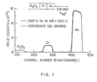
- Figs. 1 and 2 are graphs illustrating the backscattering results obtained by subjecting Au-Cr-Al 2 0 3 structures to'elevated temperatures in different atmospheres.
- the structures which are subjected to the process of the present invention include at least two layers adjacent to and in intimate contact with each other.
- One of the layers contains a first metallic-type electrical conductive material and/or semiconductor, while the other layer contains a second and different metallic-type electrical conductive material and/or semiconductor.
- the electronegativity of the first conductor and/or semiconductor is different from that of the second conductor and/or semiconductor.
- the metallic-type material can be an electrically conductive metal, mixture of electrically conductive metals, electrically conductive metallic alloy, as well as nonmetallic material, such as highly doped polysilicon or intermetallic silicides which, nevertheless, have electrical conductivities of the magnitude generally possessed by metals.
- the metallic-type layer can contain nonconducting materials as long as these do not destroy the conductivity characteristics of the layer to an undesired extent.
- metallic-type materials advantageously processed according to the present invention include gold, chromium, cobalt, copper, palladium, platinum, and aluminum.
- the present invention also contemplates treatment of layers containing semiconductive materials, such as silicon, polycrystalline silicon, and GaAs. Moreover, the layers treated can contain mixtures of metallic-type materials and semiconductors.
- the preferred structures treated according to the present invention include at least two layers which are adjacent each other and in intimate contact with each other wherein one of the layers is present on top of the other layers.
- the top layer is of a metallic-type material.
- Particular structures which are especially benefited by the present invention include those which contain an upper layer of a metal which is very resistant to oxidation, especially at elevated temperatures, such as gold, which is positioned on top of a layer of a different metallic-type material, such as chromium, cobalt or copper, or of a semiconductor, such as silicon, polycrystalline silicon, or GaAs.
- the layers can contain mixtures or alloys of these metals.
- the process is most advantageous when the structures are of relatively thin layers, such as about 10 to about 500 nm thick, and preferably about 50 to about 300 nm thick.
- Semiconductor devices employing an upper layer of gold, an intermediate layer of one or more of the other metals or semiconductors mentioned hereinabove, and a substrate of a semiconductor, such as gallium arsenide are examples of devices which can be treated according to the present invention.
- metallic electrical contacts are provided on the top surface of the gold at preselected locations and sometimes at the underside of the semiconductor substrate whereby an electrical connection between the two can be provided by means of wire.
- This processing requires the use of elevated temperatures, such as at least about 100 C, and generally up to about 500C. Most of the structures are prepared at temperatures of about 200 to about 350°C.
- the present invention is preferably concerned with treating those structures wherein the top surface is of a polycrystalline-type material.
- the gold inherently forms a polycrystalline structure when prepared according to vacuum deposition in the film thicknesses experienced according to the present invention.
- the interdiffusion can further cause the gold to migrate through the intermediate layer and through the semiconductive substrate, thereby causing short circuiting.
- the relative amount of the component gas in the mixture which changes the surface potential in the manner desired is to be sufficient so that the effect of the mixture of gases is such as to change the surface potential in the desired manner or direction (i.e., decrease or increase the work function as required).
- the preferred structures treated according to the present invention are preferably treated by positioning the structure in a chamber with the substrate resting on a support and the top surface of the upper layer facing upwards with the gas being supplied through the chamber.
- the gas upon contact with the upper surface of a polycrystalline layer, such as gold, will diffuse rapidly down to the interface, since the grain boundaries of the polycrystalline structure tend to act as pathways.
- the structures are subjected to elevated temperatures at any one time from a few minutes to about two hours, and more usually from about 10 minutes to about one hour under normal processing and/or operating conditions.
- a structure having a substrate of A1 2 0 3 upon which is provided a layer of about 200 to about 300 nm chromium and a vapor deposited layer of about 200 to about 300 nm of gold on the chromium is provided.
- the structure (the gold facing upward) is subjected to temperatures of about 250 0 C for one hour in a mixture of about 1:1 volume ratio of air and carbon monoxide.
- the structure is tested for interdiffusion by using He+ - ion backscattering spectrometry. This procedure involves counting the number of He + ions reflected back from the sample using He + at 2,8 MeV, and the counts times 10 -3 are plotted against the channel number and reproduced in Fig. 1. Also plotted in Fig. 1 is the backscattering data achieved from the same structure which has not been subjected to the elevated temperatures. As seen from Fig. 1, the 1:1 ratio of air and carbon monoxide resulted in completely stopping the interdiffusion.
- Example I is repeated except that the structure is heated in air for one hour at 250°C.
- the results obtained are presented in Fig. 2, and as apparent from Fig. 2, a comparison of that treatment with the reference shows a significant interdiffusion of the gold and chromium. Note the yield between the 300 and 400 channel numbers. As noted, for the reference within that range, the yield is about 0. On the other hand, significant yields are obtained when the heating is carried out in air.
- Example I is repeated except that the structure is heated in a mixture of about 5 parts by volume of air per 1 part by volume carbon monoxide at 250 0 C for about one hour.
- the results obtained are shown in Fig. 2.
- the air and carbon monoxide mixture of 5:1 resulted in some reduction of the interdiffusion of the gold and chromium, but not the complete elimination of such as achieved by a ratio of 1:1 of air and carbon monoxide.
Landscapes
- Electrodes Of Semiconductors (AREA)
- Internal Circuitry In Semiconductor Integrated Circuit Devices (AREA)
- Chemical Vapour Deposition (AREA)
Applications Claiming Priority (2)
| Application Number | Priority Date | Filing Date | Title |
|---|---|---|---|
| US06/124,187 US4282043A (en) | 1980-02-25 | 1980-02-25 | Process for reducing the interdiffusion of conductors and/or semiconductors in contact with each other |
| US124187 | 2002-04-17 |
Publications (3)
| Publication Number | Publication Date |
|---|---|
| EP0034785A2 true EP0034785A2 (de) | 1981-09-02 |
| EP0034785A3 EP0034785A3 (en) | 1983-09-28 |
| EP0034785B1 EP0034785B1 (de) | 1987-07-08 |
Family
ID=22413330
Family Applications (1)
| Application Number | Title | Priority Date | Filing Date |
|---|---|---|---|
| EP81101071A Expired EP0034785B1 (de) | 1980-02-25 | 1981-02-16 | Verfahren zum Reduzieren der Interdiffusion von Leitern und/oder Halbleitern im Kontakt miteinander |
Country Status (4)
| Country | Link |
|---|---|
| US (1) | US4282043A (de) |
| EP (1) | EP0034785B1 (de) |
| JP (1) | JPS56126920A (de) |
| DE (1) | DE3176304D1 (de) |
Cited By (1)
| Publication number | Priority date | Publication date | Assignee | Title |
|---|---|---|---|---|
| GB2184288A (en) * | 1985-12-16 | 1987-06-17 | Nat Semiconductor Corp | Oxidation inhibition of copper bonding pads using palladium |
Families Citing this family (5)
| Publication number | Priority date | Publication date | Assignee | Title |
|---|---|---|---|---|
| US4350993A (en) * | 1980-06-16 | 1982-09-21 | The United States Of America As Represented By The Secretary Of The Navy | Heterojunction and Schottky barrier EBS targets |
| US4709252A (en) * | 1982-07-16 | 1987-11-24 | The United States Of America As Represented By The Administrator, National Aeronautics And Space Administration | Integrated photo-responsive metal oxide semiconductor circuit |
| US4576659A (en) * | 1982-12-02 | 1986-03-18 | International Business Machines Corporation | Process for inhibiting metal migration during heat cycling of multilayer thin metal film structures |
| JPS59155950A (ja) * | 1983-02-25 | 1984-09-05 | Shinko Electric Ind Co Ltd | 半導体装置用セラミックパッケージ |
| US5374589A (en) * | 1994-04-05 | 1994-12-20 | The United States Of America As Represented By The Secretary Of The Navy | Process of making a bistable photoconductive component |
Family Cites Families (5)
| Publication number | Priority date | Publication date | Assignee | Title |
|---|---|---|---|---|
| US3982908A (en) * | 1975-11-20 | 1976-09-28 | Rca Corporation | Nickel-gold-cobalt contact for silicon devices |
| US4065588A (en) * | 1975-11-20 | 1977-12-27 | Rca Corporation | Method of making gold-cobalt contact for silicon devices |
| US4110488A (en) * | 1976-04-09 | 1978-08-29 | Rca Corporation | Method for making schottky barrier diodes |
| US4172906A (en) * | 1977-05-11 | 1979-10-30 | Rockwell International Corporation | Method for passivating III-V compound semiconductors |
| US4183781A (en) * | 1978-09-25 | 1980-01-15 | International Business Machines Corporation | Stabilization process for aluminum microcircuits which have been reactive-ion etched |
-
1980
- 1980-02-25 US US06/124,187 patent/US4282043A/en not_active Expired - Lifetime
-
1981
- 1981-01-13 JP JP276181A patent/JPS56126920A/ja active Granted
- 1981-02-16 DE DE8181101071T patent/DE3176304D1/de not_active Expired
- 1981-02-16 EP EP81101071A patent/EP0034785B1/de not_active Expired
Cited By (1)
| Publication number | Priority date | Publication date | Assignee | Title |
|---|---|---|---|---|
| GB2184288A (en) * | 1985-12-16 | 1987-06-17 | Nat Semiconductor Corp | Oxidation inhibition of copper bonding pads using palladium |
Also Published As
| Publication number | Publication date |
|---|---|
| US4282043A (en) | 1981-08-04 |
| JPH0156524B2 (de) | 1989-11-30 |
| JPS56126920A (en) | 1981-10-05 |
| EP0034785A3 (en) | 1983-09-28 |
| EP0034785B1 (de) | 1987-07-08 |
| DE3176304D1 (en) | 1987-08-13 |
Similar Documents
| Publication | Publication Date | Title |
|---|---|---|
| Murakami et al. | Microstructure studies of AuNiGe Ohmic contacts to n‐type GaAs | |
| US4056642A (en) | Method of fabricating metal-semiconductor interfaces | |
| Terry et al. | Metallization systems for silicon integrated circuits | |
| US3484313A (en) | Method of manufacturing semiconductor devices | |
| US3753774A (en) | Method for making an intermetallic contact to a semiconductor device | |
| US4725877A (en) | Metallized semiconductor device including an interface layer | |
| EP0556912B1 (de) | Verfahren zum schnellen Plasma-Hydrogenieren für MOSFET aus Polysilizium | |
| US3844924A (en) | Sputtering apparatus for forming ohmic contacts for semiconductor devices | |
| US3983264A (en) | Metal-semiconductor ohmic contacts and methods of fabrication | |
| US5227314A (en) | Method of making metal conductors having a mobile inn getterer therein | |
| US4645683A (en) | Method of manufacturing a semiconductor device | |
| JP2893723B2 (ja) | オーミック電極の製造方法 | |
| US4301188A (en) | Process for producing contact to GaAs active region | |
| US4282043A (en) | Process for reducing the interdiffusion of conductors and/or semiconductors in contact with each other | |
| US5016081A (en) | Mobile ion getterer for metal conductors | |
| US5144410A (en) | Ohmic contact for III-V semiconductor devices | |
| US3923975A (en) | Tantalum-gallium arsenide schottky barrier semiconductor device | |
| US3402081A (en) | Method for controlling the electrical characteristics of a semiconductor surface and product produced thereby | |
| US3450581A (en) | Process of coating a semiconductor with a mask and diffusing an impurity therein | |
| US5528081A (en) | High temperature refractory metal contact in silicon integrated circuits | |
| RU2086043C1 (ru) | Мощный полупроводниковый резистор и способ его изготовления | |
| Okamoto et al. | Nonalloyed ohmic contact to n-GaAs with GaS/GaAs quasi-metal-insulator-semiconductor structure | |
| Piotrowska et al. | Gold-based ohmic contacts on III–V compounds: Thermally induced reactions between metallization and the semiconductor compound | |
| Wittmer | Self‐aligned diffusion barrier by nitridation of TiSi2 | |
| US3714520A (en) | High temperature low ohmic contact to silicon |
Legal Events
| Date | Code | Title | Description |
|---|---|---|---|
| PUAI | Public reference made under article 153(3) epc to a published international application that has entered the european phase |
Free format text: ORIGINAL CODE: 0009012 |
|
| AK | Designated contracting states |
Designated state(s): DE FR GB |
|
| PUAL | Search report despatched |
Free format text: ORIGINAL CODE: 0009013 |
|
| AK | Designated contracting states |
Designated state(s): DE FR GB |
|
| 17P | Request for examination filed |
Effective date: 19840305 |
|
| GRAA | (expected) grant |
Free format text: ORIGINAL CODE: 0009210 |
|
| AK | Designated contracting states |
Kind code of ref document: B1 Designated state(s): DE FR GB |
|
| REF | Corresponds to: |
Ref document number: 3176304 Country of ref document: DE Date of ref document: 19870813 |
|
| ET | Fr: translation filed | ||
| PLBE | No opposition filed within time limit |
Free format text: ORIGINAL CODE: 0009261 |
|
| STAA | Information on the status of an ep patent application or granted ep patent |
Free format text: STATUS: NO OPPOSITION FILED WITHIN TIME LIMIT |
|
| 26N | No opposition filed | ||
| PGFP | Annual fee paid to national office [announced via postgrant information from national office to epo] |
Ref country code: GB Payment date: 19910118 Year of fee payment: 11 |
|
| PGFP | Annual fee paid to national office [announced via postgrant information from national office to epo] |
Ref country code: DE Payment date: 19910204 Year of fee payment: 11 |
|
| PGFP | Annual fee paid to national office [announced via postgrant information from national office to epo] |
Ref country code: FR Payment date: 19920124 Year of fee payment: 12 |
|
| PG25 | Lapsed in a contracting state [announced via postgrant information from national office to epo] |
Ref country code: GB Effective date: 19920216 |
|
| GBPC | Gb: european patent ceased through non-payment of renewal fee | ||
| PG25 | Lapsed in a contracting state [announced via postgrant information from national office to epo] |
Ref country code: DE Effective date: 19921103 |
|
| PG25 | Lapsed in a contracting state [announced via postgrant information from national office to epo] |
Ref country code: FR Effective date: 19931029 |
|
| REG | Reference to a national code |
Ref country code: FR Ref legal event code: ST |