EP0035111A2 - Structure and process for fabricating an integrated circuit - Google Patents
Structure and process for fabricating an integrated circuit Download PDFInfo
- Publication number
- EP0035111A2 EP0035111A2 EP81100493A EP81100493A EP0035111A2 EP 0035111 A2 EP0035111 A2 EP 0035111A2 EP 81100493 A EP81100493 A EP 81100493A EP 81100493 A EP81100493 A EP 81100493A EP 0035111 A2 EP0035111 A2 EP 0035111A2
- Authority
- EP
- European Patent Office
- Prior art keywords
- region
- conductivity type
- layer
- substrate
- epitaxial layer
- Prior art date
- Legal status (The legal status is an assumption and is not a legal conclusion. Google has not performed a legal analysis and makes no representation as to the accuracy of the status listed.)
- Granted
Links
Images


Classifications
-
- H—ELECTRICITY
- H10—SEMICONDUCTOR DEVICES; ELECTRIC SOLID-STATE DEVICES NOT OTHERWISE PROVIDED FOR
- H10D—INORGANIC ELECTRIC SEMICONDUCTOR DEVICES
- H10D10/00—Bipolar junction transistors [BJT]
- H10D10/01—Manufacture or treatment
- H10D10/051—Manufacture or treatment of vertical BJTs
-
- H—ELECTRICITY
- H10—SEMICONDUCTOR DEVICES; ELECTRIC SOLID-STATE DEVICES NOT OTHERWISE PROVIDED FOR
- H10D—INORGANIC ELECTRIC SEMICONDUCTOR DEVICES
- H10D10/00—Bipolar junction transistors [BJT]
- H10D10/40—Vertical BJTs
- H10D10/441—Vertical BJTs having an emitter-base junction ending at a main surface of the body and a base-collector junction ending at a lateral surface of the body
-
- H—ELECTRICITY
- H10—SEMICONDUCTOR DEVICES; ELECTRIC SOLID-STATE DEVICES NOT OTHERWISE PROVIDED FOR
- H10D—INORGANIC ELECTRIC SEMICONDUCTOR DEVICES
- H10D64/00—Electrodes of devices having potential barriers
- H10D64/01—Manufacture or treatment
- H10D64/011—Manufacture or treatment of electrodes ohmically coupled to a semiconductor
- H10D64/0111—Manufacture or treatment of electrodes ohmically coupled to a semiconductor to Group IV semiconductors
- H10D64/0113—Manufacture or treatment of electrodes ohmically coupled to a semiconductor to Group IV semiconductors the conductive layers comprising highly doped semiconductor materials, e.g. polysilicon layers or amorphous silicon layers
-
- H—ELECTRICITY
- H10—SEMICONDUCTOR DEVICES; ELECTRIC SOLID-STATE DEVICES NOT OTHERWISE PROVIDED FOR
- H10P—GENERIC PROCESSES OR APPARATUS FOR THE MANUFACTURE OR TREATMENT OF DEVICES COVERED BY CLASS H10
- H10P76/00—Manufacture or treatment of masks on semiconductor bodies, e.g. by lithography or photolithography
- H10P76/40—Manufacture or treatment of masks on semiconductor bodies, e.g. by lithography or photolithography of masks comprising inorganic materials
-
- H—ELECTRICITY
- H10—SEMICONDUCTOR DEVICES; ELECTRIC SOLID-STATE DEVICES NOT OTHERWISE PROVIDED FOR
- H10W—GENERIC PACKAGES, INTERCONNECTIONS, CONNECTORS OR OTHER CONSTRUCTIONAL DETAILS OF DEVICES COVERED BY CLASS H10
- H10W10/00—Isolation regions in semiconductor bodies between components of integrated devices
- H10W10/01—Manufacture or treatment
- H10W10/011—Manufacture or treatment of isolation regions comprising dielectric materials
- H10W10/014—Manufacture or treatment of isolation regions comprising dielectric materials using trench refilling with dielectric materials, e.g. shallow trench isolations
- H10W10/0143—Manufacture or treatment of isolation regions comprising dielectric materials using trench refilling with dielectric materials, e.g. shallow trench isolations comprising concurrently refilling multiple trenches having different shapes or dimensions
-
- H—ELECTRICITY
- H10—SEMICONDUCTOR DEVICES; ELECTRIC SOLID-STATE DEVICES NOT OTHERWISE PROVIDED FOR
- H10W—GENERIC PACKAGES, INTERCONNECTIONS, CONNECTORS OR OTHER CONSTRUCTIONAL DETAILS OF DEVICES COVERED BY CLASS H10
- H10W10/00—Isolation regions in semiconductor bodies between components of integrated devices
- H10W10/01—Manufacture or treatment
- H10W10/011—Manufacture or treatment of isolation regions comprising dielectric materials
- H10W10/014—Manufacture or treatment of isolation regions comprising dielectric materials using trench refilling with dielectric materials, e.g. shallow trench isolations
- H10W10/0145—Manufacture or treatment of isolation regions comprising dielectric materials using trench refilling with dielectric materials, e.g. shallow trench isolations of trenches having shapes other than rectangular or V-shape
-
- H—ELECTRICITY
- H10—SEMICONDUCTOR DEVICES; ELECTRIC SOLID-STATE DEVICES NOT OTHERWISE PROVIDED FOR
- H10W—GENERIC PACKAGES, INTERCONNECTIONS, CONNECTORS OR OTHER CONSTRUCTIONAL DETAILS OF DEVICES COVERED BY CLASS H10
- H10W10/00—Isolation regions in semiconductor bodies between components of integrated devices
- H10W10/10—Isolation regions comprising dielectric materials
- H10W10/17—Isolation regions comprising dielectric materials formed using trench refilling with dielectric materials, e.g. shallow trench isolations
-
- Y—GENERAL TAGGING OF NEW TECHNOLOGICAL DEVELOPMENTS; GENERAL TAGGING OF CROSS-SECTIONAL TECHNOLOGIES SPANNING OVER SEVERAL SECTIONS OF THE IPC; TECHNICAL SUBJECTS COVERED BY FORMER USPC CROSS-REFERENCE ART COLLECTIONS [XRACs] AND DIGESTS
- Y10—TECHNICAL SUBJECTS COVERED BY FORMER USPC
- Y10S—TECHNICAL SUBJECTS COVERED BY FORMER USPC CROSS-REFERENCE ART COLLECTIONS [XRACs] AND DIGESTS
- Y10S148/00—Metal treatment
- Y10S148/131—Reactive ion etching rie
Definitions
- This invention relates to the fabrication and structure of semiconductor devices, and, in particular, to very small integrated circuit bipolar devices with very high speed and very low power performance.
- a planar self-aligned bipolar transistor structure in which the emitter, base and collector are self-aligned.
- the structure provides in a very small discrete area of a thin epitaxial layer on a planar surface of a silicon substrate a shallow depth emitter region, a shallow depth base region and a shallow depth active collector region in the order recited.
- the small discrete area of the thin epitaxial layer has vertical sidewalls.
- Some of the more significant steps of the disclosure are heating the substrate to a temperature sufficiently high to anneal the s defects created during implantation yet sufficiently low that there is essentially no thermal diffusion or movement of impurity ions; ion implanting immediately adjacent regions to form the closely packed devices; varying the ion beam energy to implant essentially constant impurity concentration regions; ion implanting lifetime killer impurities into selected regions; ion implanting electrically neutral impurity ions into junction regions to give a steeper gradient; and ion implanting impurity ions into previously implanted regions to alter or trim the region characteristics.
- Some additional significant steps of the disclosure for obtaining narrow base regions are ion implanting into the same region both N- and P- type impurities and then heating to cause one pf the impurity types to diffuse out of the region, thereby forming a narrow base surrounding the emitter.
- the Magdo et al. patent discloses a structure useable for integrated circuits, including field effect and/or bipolar transistors, wherein a significant savings in surface area and reduction in capacitances can be obtained over prior techniques.
- the method disclosed involves forming a layer of dielectric material upon a semiconductor body, having a diffused region where a bipolar device is to be formed, and then forming an opening in the layer to expose a part of the surface of the diffused region of the semiconductor body.
- An epitaxial layer of silicon is deposited on top.
- Single crystal silicon will grow over the exposed silicon area and if a diffused region ip present in the substrate a pedestal will outdiffuse through the same area from the buried diffused region.
- Polycrystalline silicon will grow on top of the dielectrical material.
- the pedestal is formed in a single crystal epitaxial layer of another impurity type.
- Two other active elements of a bipolar transistor, such as the emitter and intrinsic base regions, are then formed in the same single crystal epitaxial layer while the inactive area, such as the extrinsic base, is formed in polycrystalline silicon.
- a reach through is made through the dielectric layer to the third element of the transistor, that is the collector region.
- the polycrystalline silicon is electrically conductive.
- Bases for bipolar transistors are formed by diffusion of an appropriate impurity into selected areas of the epitaxial layer.
- the emitters, drains, and sources are formed by diffusion of a different impurity.
- Each field effect transistor has its drain and source on adjacent parts of the epitaxial layer which are separated by the V-groove in which the gate is situated.
- the base and emitter of a bipolar transistor may be situated on one isolated part and the collector may be situated on an adjacent part separated by a V-groove having an electrically conductive polycrystalline filler.
- the Suzuki patent discloses a bipolar transistor having a heavily doped emitter region, a base region, a collector region and a passivation layer or layers on said regions.
- the passivation layer formed on a surface end of a PN junction between the collector region and the base region is a polycrystalline silicon containing oxygen atoms in a range between 14 and 35 atomic percents.
- the other passivation layer formed on a surface end of the other PN junction between the base region and the lightly doped emitter region is made of silicon dioxide which covers also a surface end of lightly doped and heavily doped junctions between the two emitter regions.
- the present trend in semiconductor technology is toward very large scale integration of devices with very high speed and low power requirements.
- the parameters that are essential to such high performance bipolar transistors are low parasitic capacitances as realized by a shallow vertical junction structure and small horizontal geometry. To achieve these goals it is necessary to make the devices in the integrated circuits as.small as possible.
- Ion implantation provides a means for precisely controlling the total amount of impurity transferred to the wafer.
- the impurity depth distribution is accurately controlled by implant energy.
- ion implantation is not a high temperature process.
- a final thermal drive-in diffusion is sufficient to anneal out the radiation damage caused by implantation, and obtain desired device junction depth. Consequently, integrated circuit devices can be made shallower, with greater precision of the impurity distribution using ion i implantation technology.
- Dielectric isolation is a method of fabricating integrated circuits in which the device components are isolated by other than P-N junctions.
- a well known dielectric isolation namely "Recessed Oxide Isolation"(ROI) is a commonly used process in present day technology.
- ROI Recessed Oxide Isolation
- Si 3 N 4 as the oxidation barrier, the ROI technique is done by etching grooves into the semiconductor wafer adjacent those regions in which PN junctions are to be formed. The silicon exposed by the grooves is then thermally oxidized to form recessed oxide regions providing dielectric isolation.
- the problem associated with the ROI is the formation of "bird's head” or “bird's beak” structure at the lateral edges of recessed oxide.
- the bird's head is undesirable because it can cause breaks or discontinuities in thin films covering the steps.
- the indefiniteness of bird's beak structure reduces the available active surface area and, therefore, imposes the need for wider tolerance of lateral dimension in the integrated circuit layout.
- a newly developed oxide isolation technique called “Deep Dielectric Isolation” (DDI) avoids the above mentioned problem.
- the DDI process utilizes reactive-ion etching (RIE) to form deep narrow trenches into the wafer surrounding those regions in which devices are to be formed.
- RIE reactive-ion etching
- DDI Integrated Circuit
- DDI Integrated Circuit
- oxide isolation With the DDT, doping processes for various device regions are then self-aligned by oxide isolation. The self-aligned process eliminates precise mask alignment steps and also saves a number of mask steps in the device fabrication.
- DDI enables us to form devices with considerably smaller cell size than those formed by using either P-N isolation or by ROI. Further reduction of device horizontal dimensions requires the use of high resolution capabilities of lithography and etching processes.
- the electron beam lithography is the most- promising method for delineating submicron size device patterns.
- the reactive ion etch is the most attractive alternative to the conventional wet solution etching.
- the RIE is a dry process having a directional etching characteristic.
- the etched device windows preserve the lithography defined etch mask dimensions, and the openings have vertical sidewalls.
- the E-beam lithography and reactive ion etching are compatible for fabricating very small device geometries.
- the base areas and, therefore, the collector-base parasitic capacitance is the most significant performance parameter.
- the active base area is the region below the emitter.
- the base contacts are formed above the inactive base area surrounding the emitter.
- the transistor base area that is needed to accommodate the emitter and base contacts is considerably larger than the active base area.
- the method for device fabrication in accordance with the invention is a self-aligned process.
- the device formed has very small vertical as well as horizontal dimensions.
- the device region is surrounded by a deep oxide trench which has nearly vertical sidewalls.
- the deep trench extends from the epitaxial silicon surface through the N+ subcollector region into the P substrate.
- the width of the deep trench is about 2pm to 3.0 ⁇ m.
- a shallow oxide trench extending from the epitaxial silicon surface to the upper portion of the N+ subcollector separates the base and collector contact.
- the surface of the dielectric isolation region and the silicon where the transistor is formed is coplanar.
- the fabricated bipolar transistor in accordance with the invention, has a mesa-type structure.
- the transistor base dimension corresponds essentially to that of the emitter. This small base area results in low collector-base capacitance which is a very important parameter in • ultra-high performance integrated circuit devices.
- Contact to the transistor base in the structure, in accordance with the invention, is achieved by a thick heavily boron doped polysilicon layer which laterally surrounds the emitter and makes lateral contact to the base.
- the P+ polysilicon layer which provides low base resistance, is formed within the oxide isolation trenches, thus minimizing the parasitic capacitance.
- the transistor active base is formed in place by a low dosage boron implantation made with its concentration peak below the emitter.
- the device thus formed will have a controllable narrow base width and a low external resistance. Both are essential to provide high speed and low power devices.
- the emitter of the structure in accordance with an embodiment of the invention is separated from the P+ polysilicon of the base contact by an SiO 2 dielectric layer or sleeve.
- This dielectric separation ensures that electrons injected into the base do occur at the bottom of the emitter.
- the dielectric sleeve of the emitter also eliminates the sidewall hole current component normally existing in conventional transistors.
- the bipolar transistor formed by the process, in accordance with the invention has a high emitter injection efficiency and also has high transistor current gains.
- the fabricated small geometry devices have planarized surfaces.
- the planarized device structure ensures the thin film covering which is critical to the integration of very small devices.
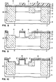
- Figure 1A is a top view of a transistor structure in accordance with the invention.
- Figure 1B is a cross-sectional view taken along the line 1B-1B of Figure lA.
- Figure 1C is a cross-sectional view taken along the line 1C-1C of Figure lA.
- Figures 2 are cross-sectional views disclosing the through 12 structure at successive stages, or steps, in the process in accordance with the invention.
- Figure 1BB is a cross-sectional view of a second or alternative transistor structure in accordance with the invention.
- Figure 1BB of the alternative transistor structure corresponds from a cross-sectional drawing viewpoint to Figure 1B of the first" transistor structure in accordance with the invention.
- Figures 2 through 6, 7A, 8, 9A, 10, 11A and 12 through 18 are respectively cross-sectional views disclosing a second or alternative transistor structure in accordance with the invention.
- a P-type monocrystalline silicon 10 is the starting substrate.
- An N-type impurity is then introduced into 10 forming the subcollector 11.
- the impurity can be any suitable N-type impurity, as for example, arsenic and can be introduced into the wafer by any suitable technique such as capsule diffusion or ion implantation.
- An N-type epitaxial silicon layer 12 is then deposited on the subcollector 11. The thickness of the epitaxial silicon 12 is about 1-2um.
- an oxide layer 13, approximately 300 nm thick, preferably deposited by CVD process is formed on epitaxial layer 12.
- a lithography step is applied to form a resist window which overlies the intended shallow trench.
- the oxide 13 defined by the resist is then opened by using reactive ion etch (RIE) technique.
- RIE reactive ion etch
- an oxide layer 15, approximately 700 nm thick, is deposited on the wafer by a CVD process. Subsequently, a lithography step is performed to form a resist window which overlies the deep trench to be fabricated. The oxide 15, defined by the resist, is then opened by RIE. Using the unetched oxide 15 as an etch mask, RIE is next used to etch through the epitaxial silicon layer 12 and subcollector 11 to form the deep trench 16. Subsequently, using a thin CVD oxide layer (not shown in Fig. 4) to protect sidewalls of the deep trench 16, a boron implantation is made to form channel stop 17 in the bottom of the deep trench.
- the wafer is thermally oxidized to form a high quality Si0 2 layer 18 over the exposed silicon surface.
- a thick oxide layer 19 formed by low pressure CVD technique is used to fill the shallow trench 14 and deep trench 16 and also planarize the wafer surface.
- a blanket resist 20 is applied and appropriately treated to further planarize the surface 19.
- the subsequent process step is to use RIE to thin back the resist layer 20 and the oxide layer 19.
- the RIE etch rate of resist is nearly equal to that of Si0 2 .
- a back-etching to silicon 12 will yield a planar surface with filled in shallow trench 21 and deep trench 22 as shown in Figure 6.
- a SiO 2 layer 23 approximately 30 nm thick, preferably formed by thermal oxidation, is grown on the silicon surface 12.
- a resist layer 24 is deposited on the wafer surface. The resist layer 24 is exposed and developed to form a block-out window 25 which overlies the intended transistor reach through region.
- a suitable N-type impurity preferably phosphorous, is ion- implanted through oxide layer 23 into the epitaxial layer 12 to form N+ reach through region 26. The resist layer 24 is subsequently stripped.
- a Si 3 N 4 layer 27 of approximately 50 nm thick is deposited on the wafer.
- a Si0 2 layer 28 is next formed on the Si 3 N 4 layer 27.
- the thickness of the SiO 2 layer 28 is approximately 300 nm.
- both S i 3 N 4 layer 27 and SiO 2 layer 28 are formed by CVD processes.
- a resist layer 29 is coated and subsequently exposed and developed to form an opening 30 which defines the intended polysilicon base contact region. Using the resist layer 29 as an etch mask, the SiO 2 layer 28, Si 3 N 4 layer 27 and SiO 2 layer 23 are etched by using an RIE process.
- CF 4/ H 2 RIE which has a very small silicon etch rate is used to etch the Si0 2 / S i 3 N 4 /Si0 2 layer.
- An RIE process which has a comparable etch rate for SiO 2 and Si is then used to etch into the epitaxial layer 12 and the oxide isolation trenches 21 and 22.
- the etched depth is determined by either the numbers of the fringes displayed by the end-point detector or by the etching time. As shown in Figure 9, the RIE etched groove 31 has nearly vertical sidewalls.
- a conformal CVD Si 3 N 4 layer 32 is deposited onto the surface of the device structure.
- a blanket RIE process is then used to directionally remove the deposited Si 3 N 4 layer 32 indicated by the dash line.
- the Si 3 N 4 layer 32 formed on the device sidewalls would not be stripped by the directional RIE.
- the exposed silicon at the bottom of the groove 31 is thermally oxidized to form a thick SiO 2 layer 33.
- the SiO 2 layer 33 is approximately 300 nm thick and, preferably, is formed by low temperature-high pressure oxidation process so as to minimize outdiffusion of the N+ buried layer 11.
- the sidewall Si 3 N 4 layer 32 is then removed by using warm H 3 P0 4 solution.
- a heavily doped P-type polysilicon layer 34 is deposited on the wafer to fill the groove.
- the polysilicon layer 34 is formed preferably by a low pressure CVD process to achieve good thickness uniformity. Doping of the polysilicon layer 34 can be done in-situ during CVD. Alternative intrinsic polysilicon can be deposited and subsequently doped by boron implantation. A resist layer 35 is next deposited and treated appropriately to obtain planarization of the wafer surface.
- the subsequent process step is to etch back the resist layer 35 and polysilicon layer 34 by RIE.
- the RIE etch rate of resist 35. is preferably equal to or slightly less than that of polysilicon 34.
- a thermal oxidation is performed to grow a relatively thick oxide layer 36 on the exposed polysilicon 34.
- the thickness of the oxide layer 36 is approximately 200 nm and preferably is formed by low temperature-high pressure oxidation process.
- the low temperature oxidation minimizes outdiffusion of P-type impurity from polysilicon 34 into the epitaxial silicon 12.
- Outdiffusion of P-type impurity forms a thin sleeve of P-region 37 in the N-type epitaxial silicon region 12. This P-region 37 is the external base of the intended transistor.
- the Si 3 N 4 layer 27 is stripped by using warm H 3 P0 4 solution.
- a conformal Si0 2 layer 38 approximately 200 nm thick is formed by CVD process.
- a resist layer 39 is next coated and subsequently exposed and developed to form a block-out window 40 defining the transistor region.
- a CF 4 /H 2 RIE is used to etch the deposited SiO 2 layer 38 and layer 23 to open the emitter contact 41 and collector contact 42.
- the side-oxide which spaces the emitter contact 41 from polysilicon 34 is thicker than that of Figure 14.
- an N-type impurity is introduced into windows 41 and 42 forming the emitter 43 and collector contact 44.
- the impurity preferably arsenic, can be introduced into the wafer by any suitable technique, as for example, capsule diffusion or ion implantation.
- a resist layer 45 is applied and subsequently exposed and developed to form a block-out window 46 for intrinsic base boron implant.
- the boron implantation is made into epitaxial layer 12.
- the energy for boron implantation is such that its concentration peak is just beyond the emitter 43.
- the block-out resist layer 45 is then stripped, and the device is heat-treated at 900°C to activate the implanted boron to form intrinsic base 47.
- a contact 48 to the P+ polysilicon is formed by lithography and an etching process. The device is then ready for metallization.
- the transistor of Figure 1BB has an improved emitter structure over that of Figure 1B by having an oxide isolated sidewall 49B around the emitter sidewall.
- the dielectric sleeve 49B of the emitter eliminates the sidewall hole current component.
- FIG. 7A For process deviation. It starts by forming a block-out resist mask 39B which defines the transistor region. An arsenic implant appropriate for forming N+ shallow emitter layer 43B is done into the wafer. This implant also provides collector reach through region 44B. After stripping the block-out resist mask 39B the wafer is then heat-treated to obtain a desired emitter • junction depth.
- the same processing steps which lead to formation of groove 31 are used for the modified structure.
- the subsequent process is to use low temperature (800-850°C) oxidation to form a 200 nm thick layer of thermal oxide 49B on the sidewalls of the N+ doped emitter layer 43B.
- the oxide 50B that is grown on the sidewalls of the N- epitaxial layer 12 by the low temperature oxidation is less than 50 nm.
- the structure is shown in Figure 9A.
- the processes that are used (earlier herein) for forming the sidewall Si 3 N 4 layer 32 and formation of thick oxide 33 at the bottom of the groove 31 are also used for the modified structure.
- the si 3 N 4 layer 32 is stripped by using H 3 PO 4 solution.
- the subsequent step is to use buffer-HF solution to etch oxide for a time more than sufficient to completely remove the thin oxide 50B formed on the sidewall-of the N- epitaxial layer 12 but still leave a substantially thick side-oxide layer 49B around the N+ emitter sidewall.
- This modified structure is shown in Figure 11A.
Landscapes
- Bipolar Transistors (AREA)
- Bipolar Integrated Circuits (AREA)
- Element Separation (AREA)
Abstract
Description
- This invention relates to the fabrication and structure of semiconductor devices, and, in particular, to very small integrated circuit bipolar devices with very high speed and very low power performance.
- A planar self-aligned bipolar transistor structure in which the emitter, base and collector are self-aligned. The structure provides in a very small discrete area of a thin epitaxial layer on a planar surface of a silicon substrate a shallow depth emitter region, a shallow depth base region and a shallow depth active collector region in the order recited. The small discrete area of the thin epitaxial layer has vertical sidewalls.
- Further encompassed, is a process and alternative process, respectively comprising a number of steps, for fabricating a structure in accordance with the invention.
- Numerous integrated circuit devices, structures and techniques of fabricating same, are known to the prior art. The following prior art patents and summaries are submitted to generally represent the state of the art.
- Reference is made to U. S. Patent No. 3,574,008 entitled "Mushroom Epitaxial Growth In Tier-Type Shaped Holes" granted April 6, 1971 to E. J. Rice. In the Rice patent, a wafer of substrate material of a given conductivity is provided. A passivating layer is then imposed upon the surface of the substrate wafer. Openings are etched in the passivating layer to expose the substrate layer, the openings having width dimensions varying from the bottom of the opening to the upper end thereof. The dimensions at the bottom of the openings are generally smaller than those at the upper end. A crystal of semiconductive material is grown epitaxially on the exposed substrate surface within the openings etched in the passivating layers. The crystals of semiconductive materials are grown until they overflow the openings onto the passivating layer and take on the appearance of mushrooms. The crystals are then lapped until the required surface condition is obtained.
- Reference is made to U. S. Patent No. 3,655,457 entitled "Method of Making or Modifying a PN-junction by Ion Implantation" granted April 11, 1972 to M. C. Duffy et al. The Duffy et al. patent discloses a method for forming integrated circuits which have closely packed devices having unique electrical and dimensional characteristics. This is accomplished by heating a semiconductor substrate to a low temperature and then ion implanting N-type, P-type, electrically neutral and lifetime killer impurities into the regions comprising the various devices. Some of the more significant steps of the disclosure are heating the substrate to a temperature sufficiently high to anneal the s defects created during implantation yet sufficiently low that there is essentially no thermal diffusion or movement of impurity ions; ion implanting immediately adjacent regions to form the closely packed devices; varying the ion beam energy to implant essentially constant impurity concentration regions; ion implanting lifetime killer impurities into selected regions; ion implanting electrically neutral impurity ions into junction regions to give a steeper gradient; and ion implanting impurity ions into previously implanted regions to alter or trim the region characteristics. Some additional significant steps of the disclosure for obtaining narrow base regions are ion implanting into the same region both N- and P- type impurities and then heating to cause one pf the impurity types to diffuse out of the region, thereby forming a narrow base surrounding the emitter.
- Reference is made to U. S. Patent No. 3,796,613 entitled "Method of Forming Dielectric Isolation for High Density Pedestal Semiconductor Devices" granted March 12, 1974 to I. E. Magdo et al. The Magdo et al. patent discloses a structure useable for integrated circuits, including field effect and/or bipolar transistors, wherein a significant savings in surface area and reduction in capacitances can be obtained over prior techniques. The method disclosed involves forming a layer of dielectric material upon a semiconductor body, having a diffused region where a bipolar device is to be formed, and then forming an opening in the layer to expose a part of the surface of the diffused region of the semiconductor body. An epitaxial layer of silicon is deposited on top. Single crystal silicon will grow over the exposed silicon area and if a diffused region ip present in the substrate a pedestal will outdiffuse through the same area from the buried diffused region. Polycrystalline silicon will grow on top of the dielectrical material. The pedestal is formed in a single crystal epitaxial layer of another impurity type. Two other active elements of a bipolar transistor, such as the emitter and intrinsic base regions, are then formed in the same single crystal epitaxial layer while the inactive area, such as the extrinsic base, is formed in polycrystalline silicon. A reach through is made through the dielectric layer to the third element of the transistor, that is the collector region.
- Reference is made to U. S. Patent No. 3,975,221 entitled "Low Capacitance V Groove NOR Gate and Method of Manufacture" granted August 17, 1976 to T. J. Rodgers. The Rodgers patent discloses a MOS transistor having a surface diffused drain and a common substrate source. A heavily doped base layer and a lightly doped space charge region are provided between the drain and source regions. The gate is formed on the inclined surface of a V groove which penetrates into the transistor to the substrate exposing the base layer to the gate structure. The gate is formed in the V groove by a silicon oxide insulative layer and conductive layer. Appropriate leads contact the gate conductor and the drain.
- Reference is made to U. S. Patent No. 4,047,217 entitled "High-Gain, High-Voltage Transistor Integrated Circuits" granted September 6, 1977 to T. McCaffrey et al. The McCaffrey patent discloses in a linear integrated circuit structure, the equivalent of a base function in a transistor, wherein the base function has a dual charge density, with the latter being relatively low in the lower active area of the base between PN junctions for high gain and high breakdown voltage, but high along the upper surface to prevent an unwanted inversion layer from occurring.
- Reference is made to U. S. Patent No. 4,048,649 entitled "Superintegrated V-Groove Isolated Bipolar and VMOS Transistors" granted September 13, 1977 to R. Bohn. The Bohn patent discloses a semiconductor structure having a compatible mixture of bipolar and unipolar transistors. In the structure, a monocrystalline P-type silicon substrate is employed which has its 1-0-0 crystallographic planes at a face on.which an n-epitaxial layer was grown. The epitaxial layer is divided into electrically isolated parts by V-grooves that extend down through the epitaxial layer and have their apices terminating in the substrate. A thin silicon dioxide film coats the V-grooves and those grooves are filled with polycrystalline silicon. Where it is desired to use the crystalline silicon as the insulated gate of a field effect transistor, the polycrystalline silicon is electrically conductive. Bases for bipolar transistors are formed by diffusion of an appropriate impurity into selected areas of the epitaxial layer. The emitters, drains, and sources are formed by diffusion of a different impurity. Each field effect transistor has its drain and source on adjacent parts of the epitaxial layer which are separated by the V-groove in which the gate is situated. The base and emitter of a bipolar transistor may be situated on one isolated part and the collector may be situated on an adjacent part separated by a V-groove having an electrically conductive polycrystalline filler.
- Reference is made to U. S. Patent No. 4,080,619 entitled "Bipolar Type Semiconductor Device" granted March 21, 1978 to K. Suzuki. The Suzuki patent discloses a bipolar transistor having a heavily doped emitter region, a base region, a collector region and a passivation layer or layers on said regions. The passivation layer formed on a surface end of a PN junction between the collector region and the base region is a polycrystalline silicon containing oxygen atoms in a range between 14 and 35 atomic percents. The other passivation layer formed on a surface end of the other PN junction between the base region and the lightly doped emitter region is made of silicon dioxide which covers also a surface end of lightly doped and heavily doped junctions between the two emitter regions.
- The present trend in semiconductor technology is toward very large scale integration of devices with very high speed and low power requirements. The parameters that are essential to such high performance bipolar transistors are low parasitic capacitances as realized by a shallow vertical junction structure and small horizontal geometry. To achieve these goals it is necessary to make the devices in the integrated circuits as.small as possible.
- With the advances in semiconductor processing technologies, such as in the fields of ion implantation, deep dielectric isolation, electron beam and x-ray lithographies, reactive ion etching, advanced insulator and polysilicon deposition techniques, and metal lift-off processes, fabrication of the ultra-high performance integrated circuit devices can be achieved.
- Ion implantation provides a means for precisely controlling the total amount of impurity transferred to the wafer. The impurity depth distribution is accurately controlled by implant energy. Unlike the conventional thermal diffusion process ion implantation is not a high temperature process. Thus, by using photoresist or metal masking, multiple impurity introduction operations can be achieved without resort to high temperatures. A final thermal drive-in diffusion is sufficient to anneal out the radiation damage caused by implantation, and obtain desired device junction depth. Consequently, integrated circuit devices can be made shallower, with greater precision of the impurity distribution using ioniimplantation technology.
- As the semiconductor devices become shallower, it is desirable to reduce the overall junction area so as to reduce parasitic capacitance. Further reduction of device parasitic capacitance can be achieved by shrinking of device horizontal dimensions and using dielectric isolation. Dielectric isolation is a method of fabricating integrated circuits in which the device components are isolated by other than P-N junctions. A well known dielectric isolation, namely "Recessed Oxide Isolation"(ROI) is a commonly used process in present day technology. Using Si3N4 as the oxidation barrier, the ROI technique is done by etching grooves into the semiconductor wafer adjacent those regions in which PN junctions are to be formed. The silicon exposed by the grooves is then thermally oxidized to form recessed oxide regions providing dielectric isolation. The problem associated with the ROI is the formation of "bird's head" or "bird's beak" structure at the lateral edges of recessed oxide. The bird's head is undesirable because it can cause breaks or discontinuities in thin films covering the steps. The indefiniteness of bird's beak structure reduces the available active surface area and, therefore, imposes the need for wider tolerance of lateral dimension in the integrated circuit layout. A newly developed oxide isolation technique called "Deep Dielectric Isolation" (DDI) avoids the above mentioned problem. The DDI process utilizes reactive-ion etching (RIE) to form deep narrow trenches into the wafer surrounding those regions in which devices are to be formed. [Reference is made to U. S. Patent No. 4,104,086, entitled "Method for Forming Isolated Regions of Silicon Utilizing Reactive Ion Etching" granted August 1, 1978 to J. A. Bondur et al., and U. S. Patent No. 4,139,442 entitled "Reactive Ion Etching Method For Producing Deep Dielectric Isolation in Silicon" granted February 13, 1979,to J. A. Bondur et al., respectively assigned to the assignee of the subject application.] The trenches are overfilled with SiO2 put down by chemical vapor deposition (CVD) technique. The overfilled SiO2 also planarizes the device surface. A blanket RIE back-etching to the semiconductor surface yields deep oxide isolation trenches. Unlike the bird's beak in ROI structures, sidewalls of the DDI structures are nearly vertical. The surface of DDI regions and the silicon where they are to be formed are coplanar. With the DDT, doping processes for various device regions are then self-aligned by oxide isolation. The self-aligned process eliminates precise mask alignment steps and also saves a number of mask steps in the device fabrication. As mentioned above, DDI enables us to form devices with considerably smaller cell size than those formed by using either P-N isolation or by ROI. Further reduction of device horizontal dimensions requires the use of high resolution capabilities of lithography and etching processes. The electron beam lithography is the most- promising method for delineating submicron size device patterns. For device window openings the reactive ion etch (RIE) is the most attractive alternative to the conventional wet solution etching. The RIE is a dry process having a directional etching characteristic. The etched device windows preserve the lithography defined etch mask dimensions, and the openings have vertical sidewalls. Thus, the E-beam lithography and reactive ion etching are compatible for fabricating very small device geometries.
- For the very.small bipolar transistor devices, as for example, micron size transistors, the base areas and, therefore, the collector-base parasitic capacitance is the most significant performance parameter. In the bipolar transistor the active base area is the region below the emitter. In the conventional transistors, fabricated in accordance with the prior art, the base contacts are formed above the inactive base area surrounding the emitter. The transistor base area that is needed to accommodate the emitter and base contacts is considerably larger than the active base area. To reduce the base area for making ultra-high performance bipolar transistors, a different approach in providing the base contact is desirable.
- It is, therefore, a primary object of the invention to provide an improved bipolar transistor having a reduced base area and a method for fabricating same. By utilizing advanced semiconductor processing techniques, the transistor structure in accordance with the invention corresponds to the indications in claim 1. An alternative structure and processing techniques in accordance with the invention result from sabclaims. The method for device fabrication in accordance with the invention, is a self-aligned process. The device formed has very small vertical as well as horizontal dimensions. The device region is surrounded by a deep oxide trench which has nearly vertical sidewalls. The deep trench extends from the epitaxial silicon surface through the N+ subcollector region into the P substrate. The width of the deep trench is about 2pm to 3.0µm. A shallow oxide trench extending from the epitaxial silicon surface to the upper portion of the N+ subcollector separates the base and collector contact. The surface of the dielectric isolation region and the silicon where the transistor is formed is coplanar.
- As shown in Figures lA, 1B, 1C (and alternatively Figure 10), the fabricated bipolar transistor, in accordance with the invention, has a mesa-type structure. The transistor base dimension corresponds essentially to that of the emitter. This small base area results in low collector-base capacitance which is a very important parameter in • ultra-high performance integrated circuit devices. Contact to the transistor base in the structure, in accordance with the invention, is achieved by a thick heavily boron doped polysilicon layer which laterally surrounds the emitter and makes lateral contact to the base. The P+ polysilicon layer, which provides low base resistance, is formed within the oxide isolation trenches, thus minimizing the parasitic capacitance. The transistor active base is formed in place by a low dosage boron implantation made with its concentration peak below the emitter. The device thus formed will have a controllable narrow base width and a low external resistance. Both are essential to provide high speed and low power devices.
- The emitter of the structure, in accordance with an embodiment of the invention is separated from the P+ polysilicon of the base contact by an SiO2 dielectric layer or sleeve. This dielectric separation ensures that electrons injected into the base do occur at the bottom of the emitter. The dielectric sleeve of the emitter also eliminates the sidewall hole current component normally existing in conventional transistors. Thus, the bipolar transistor formed by the process, in accordance with the invention, has a high emitter injection efficiency and also has high transistor current gains.
- Furthermore, the fabricated small geometry devices have planarized surfaces. The planarized device structure ensures the thin film covering which is critical to the integration of very small devices.
- The objects and advantages of the present invention will become more apparent from the following detailed description taken in conjunction with the accompanying drawings.
- • Figure 1A is a top view of a transistor structure in accordance with the invention.
- Figure 1B is a cross-sectional view taken along the line 1B-1B of Figure lA.
- Figure 1C is a cross-sectional view taken along the
line 1C-1C of Figure lA. - Figures 2 are cross-sectional views disclosing the through 12 structure at successive stages, or steps, in the process in accordance with the invention.
- Figure 1BB is a cross-sectional view of a second or alternative transistor structure in accordance with the invention. Figure 1BB of the alternative transistor structure corresponds from a cross-sectional drawing viewpoint to Figure 1B of the first" transistor structure in accordance with the invention.
- Figures 2 through 6, 7A, 8, 9A, 10, 11A and 12 through 18 are respectively cross-sectional views disclosing a second or alternative transistor structure in accordance with the invention.
- Referring now to the drawings and Fig. 2 in particular, a P-
type monocrystalline silicon 10 is the starting substrate. An N-type impurity is then introduced into 10 forming thesubcollector 11. The impurity can be any suitable N-type impurity, as for example, arsenic and can be introduced into the wafer by any suitable technique such as capsule diffusion or ion implantation. An N-typeepitaxial silicon layer 12 is then deposited on thesubcollector 11. The thickness of theepitaxial silicon 12 is about 1-2um. - As shown in Fig. 3, an
oxide layer 13, approximately 300 nm thick, preferably deposited by CVD process is formed onepitaxial layer 12. A lithography step is applied to form a resist window which overlies the intended shallow trench. Theoxide 13 defined by the resist is then opened by using reactive ion etch (RIE) technique. Using theunetched oxide layer 13 as an etch mask, the RIE is further used to etch through theepitaxial layer 12 to form ashallow trench 14. - Referring to Figure 4, an
oxide layer 15, approximately 700 nm thick, is deposited on the wafer by a CVD process. Subsequently, a lithography step is performed to form a resist window which overlies the deep trench to be fabricated. Theoxide 15, defined by the resist, is then opened by RIE. Using theunetched oxide 15 as an etch mask, RIE is next used to etch through theepitaxial silicon layer 12 andsubcollector 11 to form thedeep trench 16. Subsequently, using a thin CVD oxide layer (not shown in Fig. 4) to protect sidewalls of thedeep trench 16, a boron implantation is made to formchannel stop 17 in the bottom of the deep trench. - After stripping the CVD oxide, the wafer is thermally oxidized to form a high quality Si02 layer 18 over the exposed silicon surface. As shown in Figure 5, a
thick oxide layer 19 formed by low pressure CVD technique is used to fill theshallow trench 14 anddeep trench 16 and also planarize the wafer surface. Next a blanket resist 20 is applied and appropriately treated to further planarize thesurface 19. - Referring now to Figures 5 and 6, the subsequent process step is to use RIE to thin back the resist
layer 20 and theoxide layer 19. Of primary importance is that the RIE etch rate of resist is nearly equal to that of Si02. Thus, with an equal thickness of resist and Si02 everywhere over the wafer, a back-etching tosilicon 12 will yield a planar surface with filled inshallow trench 21 anddeep trench 22 as shown in Figure 6. - As demonstrated in Figure 7, a SiO2 layer 23, approximately 30 nm thick, preferably formed by thermal oxidation, is grown on the
silicon surface 12. A resistlayer 24 is deposited on the wafer surface. The resistlayer 24 is exposed and developed to form a block-outwindow 25 which overlies the intended transistor reach through region. A suitable N-type impurity preferably phosphorous, is ion- implanted throughoxide layer 23 into theepitaxial layer 12 to form N+ reach throughregion 26. The resistlayer 24 is subsequently stripped. - As shown in Figure 8, a Si3N4 layer 27 of approximately 50 nm thick is deposited on the wafer. A Si02 layer 28 is next formed on the Si3N4 layer 27. The thickness of the SiO2 layer 28 is approximately 300 nm. Preferably both Si3N4 layer 27 and SiO2 layer 28 are formed by CVD processes. As demonstrated in Figure 8, a resist
layer 29 is coated and subsequently exposed and developed to form anopening 30 which defines the intended polysilicon base contact region. Using the resistlayer 29 as an etch mask, the SiO2 layer 28, Si3N4 layer 27 and SiO2 layer 23 are etched by using an RIE process. Preferably, CF4/H2 RIE which has a very small silicon etch rate is used to etch the Si02/ Si3 N 4/Si02 layer. An RIE process which has a comparable etch rate for SiO2 and Si is then used to etch into theepitaxial layer 12 and theoxide isolation trenches groove 31 has nearly vertical sidewalls. - As shown in Figure 10, a conformal CVD Si3N4 layer 32, approximately 80 nm thick, is deposited onto the surface of the device structure. A blanket RIE process is then used to directionally remove the deposited Si3N4 layer 32 indicated by the dash line. The Si3N4 layer 32 formed on the device sidewalls would not be stripped by the directional RIE.
- With Si3N4 layer 32 protecting the device sidewalls, as shown in Figure 11, the exposed silicon at the bottom of the
groove 31 is thermally oxidized to form a thick SiO2 layer 33. The SiO2 layer 33 is approximately 300 nm thick and, preferably, is formed by low temperature-high pressure oxidation process so as to minimize outdiffusion of the N+ buriedlayer 11. After formation of SiO2 layer 33, the sidewall Si3N4 layer 32, is then removed by using warm H 3P04 solution. - As illustrated in Figure 12, a heavily doped P-
type polysilicon layer 34 is deposited on the wafer to fill the groove. Thepolysilicon layer 34 is formed preferably by a low pressure CVD process to achieve good thickness uniformity. Doping of thepolysilicon layer 34 can be done in-situ during CVD. Alternative intrinsic polysilicon can be deposited and subsequently doped by boron implantation. A resistlayer 35 is next deposited and treated appropriately to obtain planarization of the wafer surface. - The subsequent process step is to etch back the resist
layer 35 andpolysilicon layer 34 by RIE. The RIE etch rate of resist 35. is preferably equal to or slightly less than that ofpolysilicon 34. When the Si02 layer 28 is reached, as shown in Figure 13, the etch-back is stopped. Subsequently, the SiO2 layer 28 is stripped by using buffer-HF solution. - Referring to Figure 14, a thermal oxidation is performed to grow a relatively
thick oxide layer 36 on the exposedpolysilicon 34. The thickness of theoxide layer 36 is approximately 200 nm and preferably is formed by low temperature-high pressure oxidation process. The low temperature oxidation minimizes outdiffusion of P-type impurity frompolysilicon 34 into theepitaxial silicon 12. Outdiffusion of P-type impurity forms a thin sleeve of P-region 37 in the N-typeepitaxial silicon region 12. This P-region 37 is the external base of the intended transistor. Subsequentll, the Si3N4 layer 27 is stripped by using warm H 3P04 solution. - As shown in Figure 15, a conformal Si02 layer 38 approximately 200 nm thick is formed by CVD process. A resist
layer 39 is next coated and subsequently exposed and developed to form a block-outwindow 40 defining the transistor region. Referring to Figures 15 and 16 a CF4/H2 RIE is used to etch the deposited SiO2 layer 38 andlayer 23 to open theemitter contact 41 andcollector contact 42. As can be seen in Figure 16, the side-oxide which spaces theemitter contact 41 frompolysilicon 34 is thicker than that of Figure 14. - As demonstrated in Figure 16, an N-type impurity is introduced into
windows emitter 43 andcollector contact 44. The impurity, preferably arsenic, can be introduced into the wafer by any suitable technique, as for example, capsule diffusion or ion implantation. - Referring now to Figure 17, a resist
layer 45 is applied and subsequently exposed and developed to form a block-outwindow 46 for intrinsic base boron implant. The boron implantation is made intoepitaxial layer 12. The energy for boron implantation is such that its concentration peak is just beyond theemitter 43. The block-out resistlayer 45 is then stripped, and the device is heat-treated at 900°C to activate the implanted boron to formintrinsic base 47. - As shown in Figure 18, a
contact 48 to the P+ polysilicon is formed by lithography and an etching process. The device is then ready for metallization. - A slight modification of the process described above leads to the improved transistor structure shown in Figure 1BB. The transistor of Figure 1BB has an improved emitter structure over that of Figure 1B by having an oxide isolated sidewall 49B around the emitter sidewall. The dielectric sleeve 49B of the emitter eliminates the sidewall hole current component.
- The process modification that is needed to obtain the transistor structure of Figure 1BB is-described as follows:
- Referring to Figures 2 through 7, the initial process steps for forming the shallow 21 and deep 22 oxide isolation trenches and subsequently the formation of reach-through
phosphorus implantation region 26 are the same as those described earlier herein. - Reference is made to Figure 7A for process deviation. It starts by forming a block-out resist mask 39B which defines the transistor region. An arsenic implant appropriate for forming N+
shallow emitter layer 43B is done into the wafer. This implant also provides collector reach through region 44B. After stripping the block-out resist mask 39B the wafer is then heat-treated to obtain a desired emitter • junction depth. - Referring to Figures 8 and 9, the same processing steps which lead to formation of groove 31 (earlier herein) are used for the modified structure. The subsequent process is to use low temperature (800-850°C) oxidation to form a 200 nm thick layer of thermal oxide 49B on the sidewalls of the N+ doped
emitter layer 43B. Theoxide 50B that is grown on the sidewalls of the N-epitaxial layer 12 by the low temperature oxidation is less than 50 nm. The structure is shown in Figure 9A. - Referring to Figures 10 and 11, the processes that are used (earlier herein) for forming the sidewall Si3N4 layer 32 and formation of
thick oxide 33 at the bottom of thegroove 31 are also used for the modified structure. After formation of theoxide 33 at the bottom of the groove the si3N4 layer 32 is stripped by using H3PO4 solution. The subsequent step is to use buffer-HF solution to etch oxide for a time more than sufficient to completely remove thethin oxide 50B formed on the sidewall-of the N-epitaxial layer 12 but still leave a substantially thick side-oxide layer 49B around the N+ emitter sidewall. This modified structure is shown in Figure 11A. - The subsequent process steps which lead to the fabrication of the improved transistor structure shown in Figure 1BB are the same as set forth earlier herein (reference is made to Figures 12 through 18).
- While the invention has been particularly shown and described with reference to the preferred embodiments thereof, it will be understood by those skilled in the art that various changes in form and detail may be made therein without departing from the spirit and scope of the invention. •
Claims (7)
Applications Claiming Priority (2)
| Application Number | Priority Date | Filing Date | Title |
|---|---|---|---|
| US06/126,611 US4338138A (en) | 1980-03-03 | 1980-03-03 | Process for fabricating a bipolar transistor |
| US126611 | 1980-03-03 |
Publications (3)
| Publication Number | Publication Date |
|---|---|
| EP0035111A2 true EP0035111A2 (en) | 1981-09-09 |
| EP0035111A3 EP0035111A3 (en) | 1982-08-25 |
| EP0035111B1 EP0035111B1 (en) | 1985-10-02 |
Family
ID=22425788
Family Applications (1)
| Application Number | Title | Priority Date | Filing Date |
|---|---|---|---|
| EP81100493A Expired EP0035111B1 (en) | 1980-03-03 | 1981-01-23 | Structure and process for fabricating an integrated circuit |
Country Status (4)
| Country | Link |
|---|---|
| US (1) | US4338138A (en) |
| EP (1) | EP0035111B1 (en) |
| JP (1) | JPS56126961A (en) |
| DE (1) | DE3172466D1 (en) |
Cited By (4)
| Publication number | Priority date | Publication date | Assignee | Title |
|---|---|---|---|---|
| EP0177246A1 (en) * | 1984-09-29 | 1986-04-09 | Kabushiki Kaisha Toshiba | Heterojunction bipolar transistor and method of manufacturing the same |
| EP0152116A3 (en) * | 1984-02-15 | 1986-12-30 | Hitachi, Ltd. | Lateral bipolar transistor and method of producing the same |
| EP0098775B1 (en) * | 1982-07-01 | 1987-09-09 | Commissariat A L'energie Atomique | Process for making an integrated-circuit field oxide |
| EP0418421A1 (en) * | 1989-09-22 | 1991-03-27 | Siemens Aktiengesellschaft | Bipolar transistor having a reduced collector capacitance, and method for making the same |
Families Citing this family (49)
| Publication number | Priority date | Publication date | Assignee | Title |
|---|---|---|---|---|
| US4378630A (en) * | 1980-05-05 | 1983-04-05 | International Business Machines Corporation | Process for fabricating a high performance PNP and NPN structure |
| US4419150A (en) * | 1980-12-29 | 1983-12-06 | Rockwell International Corporation | Method of forming lateral bipolar transistors |
| JPS57149770A (en) * | 1981-03-11 | 1982-09-16 | Mitsubishi Electric Corp | Manufacture of semiconductor device |
| US4433470A (en) | 1981-05-19 | 1984-02-28 | Tokyo Shibaura Denki Kabushiki Kaisha | Method for manufacturing semiconductor device utilizing selective etching and diffusion |
| JPS57197833A (en) * | 1981-05-29 | 1982-12-04 | Nec Corp | Semiconductor device |
| JPS5835970A (en) * | 1981-08-28 | 1983-03-02 | Fujitsu Ltd | Manufacture of semiconductor device |
| US4491486A (en) * | 1981-09-17 | 1985-01-01 | Tokyo Shibaura Denki Kabushiki Kaisha | Method for manufacturing a semiconductor device |
| JPS5873156A (en) * | 1981-10-28 | 1983-05-02 | Hitachi Ltd | Semiconductor device |
| JPS5875870A (en) * | 1981-10-30 | 1983-05-07 | Hitachi Ltd | semiconductor equipment |
| US4385975A (en) * | 1981-12-30 | 1983-05-31 | International Business Machines Corp. | Method of forming wide, deep dielectric filled isolation trenches in the surface of a silicon semiconductor substrate |
| JPS58201362A (en) * | 1982-05-20 | 1983-11-24 | Toshiba Corp | Manufacture of semiconductor device |
| JPS58210634A (en) * | 1982-05-31 | 1983-12-07 | Toshiba Corp | Preparation of semiconductor device |
| JPS5940571A (en) * | 1982-08-30 | 1984-03-06 | Hitachi Ltd | Semiconductor device |
| US4819054A (en) * | 1982-09-29 | 1989-04-04 | Hitachi, Ltd. | Semiconductor IC with dual groove isolation |
| US4521952A (en) * | 1982-12-02 | 1985-06-11 | International Business Machines Corporation | Method of making integrated circuits using metal silicide contacts |
| JPS6054450A (en) * | 1983-09-05 | 1985-03-28 | Oki Electric Ind Co Ltd | Manufacture of semiconductor device |
| DE3476295D1 (en) * | 1983-09-19 | 1989-02-23 | Fairchild Semiconductor | Method of manufacturing transistor structures having junctions bound by insulating layers, and resulting structures |
| JPH0638478B2 (en) * | 1984-10-22 | 1994-05-18 | 株式会社日立製作所 | Semiconductor device |
| JP2532384B2 (en) * | 1985-01-30 | 1996-09-11 | テキサス インスツルメンツ インコ−ポレイテツド | Bipolar transistor and its manufacturing method |
| US4703554A (en) * | 1985-04-04 | 1987-11-03 | Texas Instruments Incorporated | Technique for fabricating a sidewall base contact with extrinsic base-on-insulator |
| NL8503408A (en) * | 1985-12-11 | 1987-07-01 | Philips Nv | HIGH-FREQUENCY TRANSISTOR AND METHOD OF MANUFACTURE THEREOF. |
| US4860085A (en) * | 1986-06-06 | 1989-08-22 | American Telephone And Telegraph Company, At&T Bell Laboratories | Submicron bipolar transistor with buried silicide region |
| CA1298921C (en) * | 1986-07-02 | 1992-04-14 | Madhukar B. Vora | Bipolar transistor with polysilicon stringer base contact |
| US4782030A (en) * | 1986-07-09 | 1988-11-01 | Kabushiki Kaisha Toshiba | Method of manufacturing bipolar semiconductor device |
| GB8621534D0 (en) * | 1986-09-08 | 1986-10-15 | British Telecomm | Bipolar fabrication process |
| JPS6379373A (en) * | 1986-09-24 | 1988-04-09 | Hitachi Ltd | Semiconductor device and its manufacturing method |
| JPS6381855A (en) * | 1986-09-25 | 1988-04-12 | Mitsubishi Electric Corp | Manufacturing method of heterojunction bipolar transistor |
| NL8700640A (en) * | 1987-03-18 | 1988-10-17 | Philips Nv | SEMICONDUCTOR DEVICE AND METHOD OF MANUFACTURE THEREOF |
| US4738624A (en) * | 1987-04-13 | 1988-04-19 | International Business Machines Corporation | Bipolar transistor structure with self-aligned device and isolation and fabrication process therefor |
| US4916083A (en) * | 1987-05-11 | 1990-04-10 | International Business Machines Corporation | High performance sidewall emitter transistor |
| US4847670A (en) * | 1987-05-11 | 1989-07-11 | International Business Machines Corporation | High performance sidewall emitter transistor |
| US4818713A (en) * | 1987-10-20 | 1989-04-04 | American Telephone And Telegraph Company, At&T Bell Laboratories | Techniques useful in fabricating semiconductor devices having submicron features |
| NL8800157A (en) * | 1988-01-25 | 1989-08-16 | Philips Nv | SEMICONDUCTOR DEVICE AND METHOD OF MANUFACTURE THEREOF |
| US4946798A (en) * | 1988-02-09 | 1990-08-07 | Oki Electric Industry Co., Ltd. | Semiconductor integrated circuit fabrication method |
| US4927774A (en) * | 1988-06-10 | 1990-05-22 | British Telecommunications Plc | Self aligned bipolar fabrication process |
| JPH0290617A (en) * | 1988-09-28 | 1990-03-30 | Nec Corp | Manufacture of semiconductor device |
| GB2230134A (en) * | 1989-04-05 | 1990-10-10 | Philips Nv | A method of manufacturing a semiconductor device |
| EP0476308B1 (en) * | 1990-09-20 | 1997-03-12 | Siemens Aktiengesellschaft | Bipolar transistor for high power in the microwave range |
| US5631495A (en) * | 1994-11-29 | 1997-05-20 | International Business Machines Corporation | High performance bipolar devices with plurality of base contact regions formed around the emitter layer |
| FR2756100B1 (en) * | 1996-11-19 | 1999-02-12 | Sgs Thomson Microelectronics | BIPOLAR TRANSISTOR WITH INHOMOGENEOUS TRANSMITTER IN A BICMOS INTEGRATED CIRCUIT |
| FR2756103B1 (en) * | 1996-11-19 | 1999-05-14 | Sgs Thomson Microelectronics | MANUFACTURE OF BIPOLAR / CMOS INTEGRATED CIRCUITS AND A CAPACITOR |
| FR2756974B1 (en) * | 1996-12-10 | 1999-06-04 | Sgs Thomson Microelectronics | BIPOLAR TRANSISTOR WITH INSULATION BY BOX |
| US5814547A (en) * | 1997-10-06 | 1998-09-29 | Industrial Technology Research Institute | Forming different depth trenches simultaneously by microloading effect |
| JP2001308106A (en) * | 2000-04-27 | 2001-11-02 | Mitsubishi Electric Corp | Semiconductor device and its manufacturing method |
| US6617220B2 (en) * | 2001-03-16 | 2003-09-09 | International Business Machines Corporation | Method for fabricating an epitaxial base bipolar transistor with raised extrinsic base |
| WO2004095564A1 (en) * | 2003-04-24 | 2004-11-04 | Koninklijke Philips Electronics N.V. | Method of manufacturing a semiconductor device with a bipolar transistor |
| GB0507157D0 (en) * | 2005-04-08 | 2005-05-18 | Ami Semiconductor Belgium Bvba | Double trench for isolation of semiconductor devices |
| US8932931B2 (en) | 2012-02-13 | 2015-01-13 | International Business Machines Corporation | Self-aligned emitter-base region |
| US10593771B2 (en) * | 2017-12-11 | 2020-03-17 | International Business Machines Corporation | Vertical fin-type bipolar junction transistor with self-aligned base contact |
Family Cites Families (18)
| Publication number | Priority date | Publication date | Assignee | Title |
|---|---|---|---|---|
| US3655457A (en) * | 1968-08-06 | 1972-04-11 | Ibm | Method of making or modifying a pn-junction by ion implantation |
| US3574008A (en) * | 1968-08-19 | 1971-04-06 | Trw Semiconductors Inc | Mushroom epitaxial growth in tier-type shaped holes |
| US3796613A (en) * | 1971-06-18 | 1974-03-12 | Ibm | Method of forming dielectric isolation for high density pedestal semiconductor devices |
| US3975221A (en) * | 1973-08-29 | 1976-08-17 | American Micro-Systems, Inc. | Low capacitance V groove MOS NOR gate and method of manufacture |
| JPS51128269A (en) * | 1975-04-30 | 1976-11-09 | Sony Corp | Semiconductor unit |
| US4048649A (en) * | 1976-02-06 | 1977-09-13 | Transitron Electronic Corporation | Superintegrated v-groove isolated bipolar and vmos transistors |
| JPS52103971A (en) * | 1976-02-26 | 1977-08-31 | Nec Corp | Semiconductor device |
| US4047217A (en) * | 1976-04-12 | 1977-09-06 | Fairchild Camera And Instrument Corporation | High-gain, high-voltage transistor for linear integrated circuits |
| JPS5328384A (en) * | 1976-08-27 | 1978-03-16 | Fujitsu Ltd | Production method of semiconductor device |
| US4115797A (en) * | 1976-10-04 | 1978-09-19 | Fairchild Camera And Instrument Corporation | Integrated injection logic with heavily doped injector base self-aligned with injector emitter and collector |
| US4104086A (en) * | 1977-08-15 | 1978-08-01 | International Business Machines Corporation | Method for forming isolated regions of silicon utilizing reactive ion etching |
| US4139442A (en) * | 1977-09-13 | 1979-02-13 | International Business Machines Corporation | Reactive ion etching method for producing deep dielectric isolation in silicon |
| JPS54128683A (en) * | 1978-03-27 | 1979-10-05 | Ibm | Method of fabricating emitterrbase matching bipolar transistor |
| US4157269A (en) * | 1978-06-06 | 1979-06-05 | International Business Machines Corporation | Utilizing polysilicon diffusion sources and special masking techniques |
| US4242791A (en) * | 1979-09-21 | 1981-01-06 | International Business Machines Corporation | High performance bipolar transistors fabricated by post emitter base implantation process |
| JPS5667765U (en) * | 1979-10-29 | 1981-06-05 | ||
| US4252582A (en) * | 1980-01-25 | 1981-02-24 | International Business Machines Corporation | Self aligned method for making bipolar transistor having minimum base to emitter contact spacing |
| JPS625349A (en) * | 1985-07-02 | 1987-01-12 | 株式会社新素材総合研究所 | Liquid container |
-
1980
- 1980-03-03 US US06/126,611 patent/US4338138A/en not_active Expired - Lifetime
-
1981
- 1981-01-19 JP JP523681A patent/JPS56126961A/en active Granted
- 1981-01-23 DE DE8181100493T patent/DE3172466D1/en not_active Expired
- 1981-01-23 EP EP81100493A patent/EP0035111B1/en not_active Expired
Cited By (4)
| Publication number | Priority date | Publication date | Assignee | Title |
|---|---|---|---|---|
| EP0098775B1 (en) * | 1982-07-01 | 1987-09-09 | Commissariat A L'energie Atomique | Process for making an integrated-circuit field oxide |
| EP0152116A3 (en) * | 1984-02-15 | 1986-12-30 | Hitachi, Ltd. | Lateral bipolar transistor and method of producing the same |
| EP0177246A1 (en) * | 1984-09-29 | 1986-04-09 | Kabushiki Kaisha Toshiba | Heterojunction bipolar transistor and method of manufacturing the same |
| EP0418421A1 (en) * | 1989-09-22 | 1991-03-27 | Siemens Aktiengesellschaft | Bipolar transistor having a reduced collector capacitance, and method for making the same |
Also Published As
| Publication number | Publication date |
|---|---|
| EP0035111A3 (en) | 1982-08-25 |
| EP0035111B1 (en) | 1985-10-02 |
| US4338138A (en) | 1982-07-06 |
| DE3172466D1 (en) | 1985-11-07 |
| JPH0158668B2 (en) | 1989-12-13 |
| JPS56126961A (en) | 1981-10-05 |
Similar Documents
| Publication | Publication Date | Title |
|---|---|---|
| EP0035111B1 (en) | Structure and process for fabricating an integrated circuit | |
| US4333227A (en) | Process for fabricating a self-aligned micrometer bipolar transistor device | |
| US4318751A (en) | Self-aligned process for providing an improved high performance bipolar transistor | |
| CA1273128A (en) | Process for manufacturing semiconductor bicmos devices | |
| US4378630A (en) | Process for fabricating a high performance PNP and NPN structure | |
| US4733287A (en) | Integrated circuit structure with active elements of bipolar transistor formed in slots | |
| US4339767A (en) | High performance PNP and NPN transistor structure | |
| US4303933A (en) | Self-aligned micrometer bipolar transistor device and process | |
| US4392149A (en) | Bipolar transistor | |
| US4415371A (en) | Method of making sub-micron dimensioned NPN lateral transistor | |
| US4853342A (en) | Method of manufacturing semiconductor integrated circuit device having transistor | |
| US4900689A (en) | Method of fabrication of isolated islands for complementary bipolar devices | |
| EP0108204B1 (en) | Method for diffusing impurities and semiconductor devices fabricated by said method | |
| US3956033A (en) | Method of fabricating an integrated semiconductor transistor structure with epitaxial contact to the buried sub-collector | |
| US5374846A (en) | Bipolar transistor with a particular base and collector regions | |
| US5154946A (en) | CMOS structure fabrication | |
| US4001048A (en) | Method of making metal oxide semiconductor structures using ion implantation | |
| US4969026A (en) | Mesa bipolar transistor with edge contacts | |
| US6362025B1 (en) | Method of manufacturing a vertical-channel MOSFET | |
| EP0337720B1 (en) | Method for fabricating a bipolar transistor | |
| EP0036499B1 (en) | A polysilicon-base self-aligned bipolar transistor process | |
| KR100762523B1 (en) | Method of manufacturing an improved semiconductor trench MOS device | |
| EP0253538A2 (en) | A VLSI self-aligned bipolar transistor | |
| KR100246653B1 (en) | Manufacturing Method of CMOS Structure | |
| US20030042574A1 (en) | Contact structure on a deep region formed in a semiconductor substrate |
Legal Events
| Date | Code | Title | Description |
|---|---|---|---|
| PUAI | Public reference made under article 153(3) epc to a published international application that has entered the european phase |
Free format text: ORIGINAL CODE: 0009012 |
|
| AK | Designated contracting states |
Designated state(s): DE FR GB IT |
|
| 17P | Request for examination filed |
Effective date: 19811020 |
|
| PUAL | Search report despatched |
Free format text: ORIGINAL CODE: 0009013 |
|
| AK | Designated contracting states |
Designated state(s): DE FR GB IT |
|
| ITF | It: translation for a ep patent filed | ||
| GRAA | (expected) grant |
Free format text: ORIGINAL CODE: 0009210 |
|
| AK | Designated contracting states |
Designated state(s): DE FR GB IT |
|
| REF | Corresponds to: |
Ref document number: 3172466 Country of ref document: DE Date of ref document: 19851107 |
|
| ET | Fr: translation filed | ||
| PLBE | No opposition filed within time limit |
Free format text: ORIGINAL CODE: 0009261 |
|
| STAA | Information on the status of an ep patent application or granted ep patent |
Free format text: STATUS: NO OPPOSITION FILED WITHIN TIME LIMIT |
|
| 26N | No opposition filed | ||
| PGFP | Annual fee paid to national office [announced via postgrant information from national office to epo] |
Ref country code: GB Payment date: 19901220 Year of fee payment: 11 |
|
| ITTA | It: last paid annual fee | ||
| PGFP | Annual fee paid to national office [announced via postgrant information from national office to epo] |
Ref country code: DE Payment date: 19910131 Year of fee payment: 11 |
|
| PGFP | Annual fee paid to national office [announced via postgrant information from national office to epo] |
Ref country code: FR Payment date: 19911218 Year of fee payment: 12 |
|
| PG25 | Lapsed in a contracting state [announced via postgrant information from national office to epo] |
Ref country code: GB Effective date: 19920123 |
|
| REG | Reference to a national code |
Ref country code: GB Ref legal event code: PCNP |
|
| PG25 | Lapsed in a contracting state [announced via postgrant information from national office to epo] |
Ref country code: DE Effective date: 19921001 |
|
| PG25 | Lapsed in a contracting state [announced via postgrant information from national office to epo] |
Ref country code: FR Effective date: 19930930 |
|
| REG | Reference to a national code |
Ref country code: FR Ref legal event code: ST |