EP0035350A1 - Dispositif logique supraconducteur comprenant une jonction de Josephson - Google Patents
Dispositif logique supraconducteur comprenant une jonction de Josephson Download PDFInfo
- Publication number
- EP0035350A1 EP0035350A1 EP81300724A EP81300724A EP0035350A1 EP 0035350 A1 EP0035350 A1 EP 0035350A1 EP 81300724 A EP81300724 A EP 81300724A EP 81300724 A EP81300724 A EP 81300724A EP 0035350 A1 EP0035350 A1 EP 0035350A1
- Authority
- EP
- European Patent Office
- Prior art keywords
- superconductive
- counter electrode
- ground plane
- current
- insulating layer
- Prior art date
- Legal status (The legal status is an assumption and is not a legal conclusion. Google has not performed a legal analysis and makes no representation as to the accuracy of the status listed.)
- Granted
Links
Images






Classifications
-
- H—ELECTRICITY
- H10—SEMICONDUCTOR DEVICES; ELECTRIC SOLID-STATE DEVICES NOT OTHERWISE PROVIDED FOR
- H10N—ELECTRIC SOLID-STATE DEVICES NOT OTHERWISE PROVIDED FOR
- H10N60/00—Superconducting devices
- H10N60/10—Junction-based devices
- H10N60/12—Josephson-effect devices
-
- Y—GENERAL TAGGING OF NEW TECHNOLOGICAL DEVELOPMENTS; GENERAL TAGGING OF CROSS-SECTIONAL TECHNOLOGIES SPANNING OVER SEVERAL SECTIONS OF THE IPC; TECHNICAL SUBJECTS COVERED BY FORMER USPC CROSS-REFERENCE ART COLLECTIONS [XRACs] AND DIGESTS
- Y10—TECHNICAL SUBJECTS COVERED BY FORMER USPC
- Y10S—TECHNICAL SUBJECTS COVERED BY FORMER USPC CROSS-REFERENCE ART COLLECTIONS [XRACs] AND DIGESTS
- Y10S505/00—Superconductor technology: apparatus, material, process
- Y10S505/825—Apparatus per se, device per se, or process of making or operating same
- Y10S505/873—Active solid-state device
- Y10S505/874—Active solid-state device with josephson junction, e.g. squid
Definitions
- the present invention rel tes to'a superconductive logic device and, more particularly, to a superconductive logic device incorporating a Josephson junction which can be, for example, used for digital computers.
- a Josephson junction comprises two superconductive layers with a thin insulating layer therebetween, which is so thin that superconductive electrons can pass therethrough.
- the Josephson junction serves as a switching device, wherein a critical current of the junction is controlled by acting on the junction with a magnetic field.
- a first conventional superconductive logic device incorporating Josephson junctions comprises a superconductive ground plane, a superconductive base electrode, a superconductive counter electrode which is opposed to the base electrode, and a superconductive control line.
- the above--mentioned superconductive elements are electrically insulated from each other.
- the base and counter electrodes form a Josephson junction in association with a thin insulating layer therebetween.
- the control line extends over the junction.
- the first conventional device is called a magnetic field coupled type gate which is disclosed in J. Matisoo, "The Tunneling Cryotron - A Superconductive Logic Element Based on Electron Tunneling," Proc. IEEE Vol. 55 No. 2 Feb. (1967) pp. 172-180 (in particular, Fig. 3).
- the junction has a voltage state and a zero-voltage state.
- the two states are switched by changing a magnetic field induced by an input signal current flowing through the control line, or by changing a bias current which is supplied from the base electrode and flows through the junction to the counter electrode.
- the first superconductive logic device incorporating Josephson junctions can serve as a switching device.
- a second conventional superconductive logic device incorporating Josephson junctions comprises a superconductive ground plane, a superconductive base electrode and a superconductive counter electrode, which are also electrically insulated.
- the base electrode serves also as a control line. Therefore, the number of layers are reduced and accordingly, the amount of the manufacturing cost is reduced, as compared with the first conventional device. In addition, the number of disconnections and short circuits generated in the stepped portions is reduced as compared with the first conventional device.
- the second conventional device is called a current injection logic type (CIL) which is disclosed in T.R. Gheewala "A 30-ps Josephson Current Injection Logic (CIL)," IEEE J. Solid-State Circ. Vol. SC-14, No. 5, pp. 787-793, Oct.
- a superconductive logic device comprising: a superconductive ground plane; a first insulating layer overlying the superconductive ground plane; a superconductive base electrode, for receiving a bias current, formed on the first insulating layer; second and third insulating layers formed on the superconductive base electrode, the second insulating layer being thicker than the third insulating layer; and a superconductive counter electrode formed on the second and third insulating layers such that at least one Josephson junction is formed by the superconductive base electrode, the counter electrode and the third insulating layer therebetween; the device characterized in that the superconductive counter electrode comprises a first extension electrically connected to the superconductive ground plane, and a second extension serving as an input terminal for an input signal.
- the device may further comprise an oxidation-resisting, low-resistance material layer between the superconductive ground plane and the first superconductive counter electrode extension.
- the counter electrode may be formed in two parts, a first part including the said second extension and a second part partially overlapping the first part and including the said first extension for connecting the superconductive counter electrode to the superconductive ground plane.
- the base electrode When used as an OR device, the base electrode is preferably T-shaped and has a leg portion for receiving a bias current; the said third insulating layer is located at each side of an arm portion of the T-shaped superconductive base electrode, the superconductive counter electrode formed on the second and third insulating layers having two extensions for receiving two input signals, extending over the arm portion of the T-shaped superconductive counter electrode, and having one extension located at an intermediate position thereof and connected to the superconductive ground plane; and at least two Josephson junctions are formed by the T-shaped superconductive base electrode, the superconductive counter electrode and the third insulating layer therebetween.
- the base electrode When used as a flip-flop, the base electrode is preferably forked and has a leg portion for receiving the bias current; the third insulating layer is located over both arm portions of the forked superconductive base electrode, and two L-shaped superconductive counter electrodes are formed on the second and third insulating layers, each having a first extension for receiving an input signal and a second extension connected to the superconductive ground plane; at least two Josephson junctions being formed by the forked superconductive base electrode, the said L-shaped superconductive counter electrodes and the third insulating layer therebetween.
- Logic devices incorporating the invention may include a plurality of Josephson junctions connected in series with a resistor, all connected in parallel to the same output terminal, and using the same ground plane.
- the devices advantageously include a plurality of parallel input terminals and parallel output terminals.
- Fig. 1A is a perspective view partly in section illustrating a first conventional superconductive logic device
- a superconductive ground plane 2 is formed on an insulating substrate 1 which is, for example, silicon.
- insulating substrate 1 which is, for example, silicon.
- the electrodes 4 and 7 are electrically insulated by a relatively thick insulating layer 5 and a relatively thin insulating layer 6.
- the thin insulating layer 6 is so thin that superconductive electrons can pass therethrough. Therefore, the electrodes 4 and 7 in association with the thin insulating layer 6 form a Josephson junction.
- insulating layer 5 and the counter electrode 7 there is formed another relatively thick insulating layer 8 on which a superconductive control line 9 is formed.
- the superconductive elements 2, 4, 7 and 9 are made of, for example, niobium or lead, while the insulating layers 3, 5, 6 and 8 are made of, for example, SiO.
- the Josephson junction comprised of the electrodes 4 and 7 and the insulating layer 6 has voltage (V) to current (I) characteristics as illustrated in Fig. 1B.
- V voltage
- I current
- Fig. 1C is an equivalent circuit diagram of the superconductive logic device of Fig. lA.
- J indicates the Josephson junction comprised of the base electrode 4, the insulating layer 6 and the counter electrode 7 in Fig. lA.
- a circuit of the Josephson junction J is independent of and separated from a circuit for the-input signal current I H . Therefore, isolation between the input and output signals is easy. In this case, the output signals are obtained at the terminals OUT1 and OUT2, that is, the electrodes 4 and 7.
- the device is of a multi-layer structure wherein a large number of layers are provided. Therefore, a number of manufacturing steps is large which requires a high cost. In addition, a difficulty arises, from the manufacturing point of view, in that, for example, disconnections and short circuits are often generated.
- Fig. 2A is a perspective view partly in section illustrating a second conventional superconductive logic device incorporating Josephson junctions.
- the elements which are the same as those of Fig. lA, are denoted by the same reference numerals.
- a control line 10 is combined with the base electrode 4.
- the control line 10 and the base electrode 4 are manufactured simultaneously at the same manufacturing step. Therefore, since two layers, that is, the insulating layer 8 and the control line 9 in Fig. 1 are omitted, the number of manufacturing steps is reduced and the number of disconnections or short circuits during the manufacturing processes can be reduced as compared with the first conventional device of Fig. lA.
- Fig. 2B is an equivalent circuit diagram of the superconductive logic device of Fig. 2A.
- the switching of the voltage and zero-voltage states is dependent upon I > I or I ⁇ I C , where I is an element current flowing through the Josephson junction J and I C is a critical current of the junction J.
- the former corresponds to the voltage state, while the latter corresponds to the zero-voltage state.
- the element current I is represented by I H + I B . Therefore, such switching may be effected by changing the element current I, instead of changing the magnetic field generated in the junction J, that is, the critical current I C .
- the input signal current I H flowing through the control line 9 acts upon the Josephson junction with a magnetic field, so that the critical current I C of the junction is changed.
- Fig. 3 which is an enlarged cross-sectional view of the Josephson junction portion of Fig. lA
- the thickness ⁇ L of the current flowing surface region is called London's penetration depth.
- the current I H causes a current I 1 to flow on the surface of the counter electrode 7, so that no magnetic field is generated in the superconductive counter electrode 7.
- the current I I is called an image current.
- currents 1 2 and I 3 which are also image currents flow on the surfaces of the base electrode 4 and the ground plane 2, respectively, so that no magnetic fields are generated in the superconductive base electrode 4 and the superconductive ground plane 2.
- the magnitudes of the image currents I 1 , 1 2 and I 3 are almost the same as the input signal current I H . For example, if there is no space between the ground plane 2, the electrodes 4 and 7, and the control line 9, each of the image currents I 1 , I 2 and I 3 is equal to the input signal current I H .
- each of the image currents I 1 , I 2 and I3 is a little smaller than the input signal current I H .
- the input signal-current I H is almost equal to the image current I 1 flowing on the upper surface of the counter electrode 7, which currents are flowing in an opposite direction to each other, the two magnetic fields induced by the two currents I H and I 1 contradict each other.
- the image current 1 2 flowing on the lower surface of the base electrode 4 is almost equal to the image current 1 3 flowing on the upper surface of the ground plane 2, which currents are flowing in an opposite direction to each other, and the two magnetic fields induced by the two currents I 2 and 1 3 also contradict each other.
- the magnetic field in the Josephson junction which corresponds to the insulating layer 6 is determined by only two currents, that is, the image current I 1 flowing on the lower surface of the counter electrode 7 and the image current 1 2 on the upper surface of the base electrode 4. In other words, if the current I 1 can flow through the lower surface of the counter electrode 7, the ground plane 2 and the control line 9 are unnecessary. However, it should be noted that the ground plane 2 is indispensable for generating a magnetic field effectively in the Josephson junction.
- the present invention is based on such an idea that, if the current I 1 can flow on the lower surface of the counter electrode 7, the control line 9 can be omitted.
- a counter electrode direct-coupled type logic device in which a counter electrode serves also as a control line and is connected electrically and directly to a ground plane.
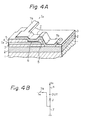
- Fig. 4A is a perspective view partly in section illustrating a first embodiment of the superconductive logic device according to the present invention.
- the elements which are the same as those of Fig. 1A are denoted by the same reference numerals.
- the insulating layer 8 and the control line 9 in Fig. 1A are not provided. That is, in the counter electrode 7, one counter electrode extension 7a serves as an input terminal for the input signal current I H , while the other counter electrode extension 7b is connected directly to the ground plane 2 and, therefore, is grounded. Therefore, the input signal current I H is supplied from the counter electrode extension 7a and flows on the lower surface of the counter electrode 7 to the ground plane 2, not through the Josephson junction.
- Fig. 4B is an equivalent circuit diagram of the superconductive logic device of Fig. 4A.
- a circuit for the input signal current I H is independent of and separated from a circuit of the Josephson junction J, so that isolation between input and output components is easy.
- an output signal which is obtained at an output terminal OUT does not include the component of the input signal current I H .
- Fig. 4C is a cross-sectional view of the Josephson junction portion of Fig. 4A.
- the current I H flows on-the lower surface of the counter electrode 7 including its extension 7b to the upper surface of the ground plane 2.
- image current 1 2 whose value is a little smaller than the input signal current I H flows on the surface of the base electrode 4.
- the input signal current I H generates image currents which, in turn, generate the magnetic field in the junction; however, in Fig. 4C, the input signal current I directly generates the magnetic field in the junction. Therefore, the magnetic field in the junction of Fig. 4C becomes large as compared with that of Fig. 3.
- Fig. 5, 6 and 7 are perspective views partly in section illustrating second, third and fourth embodiments of the superconductive logic device according to the present invention, respectively.
- the elements which are the same as those of Fig. 4A are denoted by the same reference numerals.
- an oxidization-resisting and low resistance material layer 11 is inserted between the ground plane 2 and the counter electrode extension 7b
- an oxidization--resisting and low resistance material layer 12 is inserted between the ground plane 2 and the insulating layer 3.
- another superconductive layer 13 which connects the counter electrode 7 to the ground plane 2 is provided.
- Figs. 8(1) through 8(7) are cross-sectional views for explaining the manufacturing steps of the device of Fig. 5.
- a superconductive material such as niobium (Nb) is deposited as a ground plane 2 with a thickness of 200 to 300 nm an insulating substrate 1 which is made of silicon or glass.
- silicon oxide (SiO) is deposited as an insulating layer 3 with a thickness of 200 nm on the ground plane 2.
- the patterning of the insulating layer 3 is made by a lift-off process or an etching process. After that, oxide and contamination on the exposed surface of the ground plane 2 are removed by sputter etching in argon.
- an oxidization-resisting and low resistance material such as gold (Au) or gold-indium (Au-In), where in the gold component thereof is large, is deposited as a layer 11 with a thickness of 200 nm on the exposed surface of the ground plane 2, that is, the contact hole of the insulator 3.
- the resistance of the layer 11 is about 10 -4 ⁇ , which is much less than the normal resistance of the Josephson junction, since the layer has a relatively large area and is small in thickness. Therefore, even when a current whose value is 10 mA flows through the layer 11, the voltage drop induced by the layer 11 is on the order of less than 10 of the normal voltage of the junction, which causes no problem.
- SiO of a 300 nm thickness indicated by reference 5 is deposited and patterned so as to demarcate the junction area by a lift-off process or an etching process.
- the junction area of the base electrode 4 is again oxidized by an RF plasma oxidization process, so that an insulating layer 6 which is made of (PbO + In 2 0 3 ) of about 3 nm thickness is formed.
- the insulating layer 6 constitutes the afore-mentioned Josephson junction.
- a counter electrode 7 is formed by successively evaporating lead (Pb) of a 200 nm thickness, gold (Au).. of an 8 nm thickness and lead (Pb) of a 200 nm. thickness in this order.
- the patterning of this evaporated layer is made by a lift-off process.
- the deposition process of an oxidization-resisting and low resistance layer 12 which is, for example, gold (Au) of a 10 nm thickness, is added after the step as illustrated in Fig. 8(1).
- Au gold
- each thickness of the above-mentioned gold layers 11 (Fig. 5) and 12 (Fig. 6) must be small enough as compared with a penetration depth (skin depth) X of the magnetic field for the highest frequency signal.
- the manufacturing steps of the device of Fig. 7 are the same as those of the device of Fig. 4A, except for an additional manufacturing step for depositing an additional superconductive layer 13.
- the present invention can be also applied to a superconducting quantum interference device (SQUID) with two or more junctions, which is illustrated in Figs. 9A and 10A.
- SQUID superconducting quantum interference device
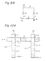
- Fig. 9A is a perspective view partly in section illustrating a fifth embodiment of the superconductive logic device according to the present invention.
- a SQUID with two junctions using the device of Fig. 4A is illustrated. That is, two insulating layers 6a and 6b which are the same as the insulating layer 6 of Fig. 4A are provided so as to form two Josephson junctions.
- An input signal current I H flows from the counter electrode extension 7a, through the counter electrode 7 over the two junctions which correspond to the layers 6a and 6b to the ground plane 2.
- Fig. 9B is an equivalent circuit diagram of the device of Fig. 9A.
- L is an inductance existing in the counter electrode 7 between the two junctions.
- SQUID as illustrated in Figs. 9A and 9B has a higher sensitivity as compared with the device with one junction of Fig. 4A, 5, 6 or 7, so that each of the junctions J a and i b can be reduced, in other words, each of the layers 6a and 6b can be small in area.
- Fig. 10A is a plan view illustrating a sixth embodiment of the superconductive logic device according to the present invention and Fig. 10B is an equivalent circuit diagram of the device of F ig. 10A.
- Fig. 10A two SQUIDs SQ-1 and SQ-2 are connected by a load resistor 14. Each of the SQUIDs SQ-1 and SQ-2 are the same as the SQUID of Fig. 9A.
- contact holes CON T -1 and CONT-2 are used for connecting the counter electrodes 7-1 and 7-2, respectively, to the ground plane 2 (not shown).
- Fig. 11 is an equivalent circuit diagram illustrating a seventh embodiment of the superconductive logic device according to the present invention.
- Fig. 11 which is similar to Fig. 4B, three input terminals IN-I, IN-2 and . IN-3 are provided so as to perform an OR or AND logic operation for three input signal currents I H1 , I H2 and I H3'
- the input terminals IN-1, IN-2 and IN-3 are connected to three counter electrode extensions 7a-1, 7a-2 and 7a-3 which are the same as the counter electrode extension 7a of Fig. 4A, 5, 6 or 7.
- an OR logic operation can be effected for the three input signals I H1 , I H2 and I H3 .
- an arbitrary number of output terminals or output circuits can be provided, as long as a division output current at each output terminal can drive a next-stage gate.
- the counter electrode since the counter electrode is connected to the ground plane, it is necessary to arrange the output circuits in parallel. If the output circuits are arranged in series, the potential of a point for connecting the output circuits to the counter electrode is changed, so that the counter electrode can not be grounded. In other words, an input signal current I H leaks into the output circuits.
- each output current is reduced by a factor of n.
- Fig. 12 is an equivalent circuit diagram illustrating an eighth embodiment of the superconductive logic device according to the present invention. In this embodiment, the above-mentioned problem is eliminated.
- Fig. 12 which is similar to Fig. 4B, two resistors r and r 2 are provided for dividing the bias current I B , and R 1 and R 2 are resistances of two output circuits.
- a Josephson junction J 1 is the same as the counter electrode direct-coupled type Josephson junction J of Fig. 4B which receives an input signal current I H , while a Josephson junction J 2 does not require the input signal current I .
- each of the output currents I 01 and 1 02 is almost half of the bias current I B , which is, however, twice as large as the bias current I B in the circuit of Fig. 4B.
- the counter electrode direct-coupled device with twice the driving ability for output circuits can be obtained.
- the SQUID with two junctions of Figs. 9A and 9B or the device with more than two junctions can be used instead of the Josephson junction J l .
- n parallel circuits each of which is comprised of the junction J 2 and the resistor r 2 are arranged in parallel in Fig. 12, the counter electrode direct-coupled device with n times as large a driving ability for output circuits can be obtained. Therefore, in this case, n output circuits can be provided.
- the counter electrode direct-coupled type Josephson device according to the present invention can be applied to various kinds of logic gates, such as an exclusive OR (hereinafter referred to as EXOR) logic gate, an OR logic gate or a flip-flop circuit.
- EXOR exclusive OR
- OR OR logic gate
- Fig. 13A is a plan view illustrating a ninth embodiment of the superconductive logic device according to the present invention, which is used for performing an EXOR logic operation.
- Figs. 13B and 13C are cross-sectional views taken along the lines B-B and the lines C-C, respectively, of Fig. 13A.
- two Josephson junctions are formed by a base electrode 4, a counter electrode 7 and two insulating layers 6-1 and 6-2, and the counter electrode 7 is also grounded by connecting its extension 7b to a ground plane 2.
- the base electrode 4 is T-shaped and, in addition, the counter electrode 7 extends over the arm portion of the base electrode 4. Further, the insulating layers 6-1 and 6-2 are located at both sides of the arm portion. Two extensions 7a-1 and 7a-2 of the counter electrode 7 serve as input terminals for two input signal currents I H1 and I H2 , while the leg portion of the base electrode 4 serves as an input terminal for a bias current I B , as well as an output terminal.
- the bias current I B flows from the leg portion of the base electrode 4 through the arm portion thereof, continuing through the insulating layers 6-1 and 6-2, the counter electrode 7 and its extension 7b to the ground plane 2.
- the current I B is selected so as to make both of the junctions be in the zero-voltage state when the input signal currents I H1 and I H2 are both zero.
- the input signal currents I H1 and I H2 flow from the extensions 7a-1 and 7a-2 of the counter electrode 7 through the extension 7b to the ground plane 2.
- Fig. 13D is an equivalent circuit diagram of the device of Fig. 13A. As is understood from Fig. 13D, the function of the input signal current I H1 or I H2 is similar to that of a so-called DC SQUID which is illustrated in Figs. 9A and 9B, except for two input terminals.
- the bias current I B is supplied. This is because if one of the input signal currents I H1 and I H2 flows at the same time that the bias current I B flows, the junctions J 1 and J 2 become in the voltage state and, after that, even when the other current flows, the junctions remain in the voltage state by which an EXOR operation is not performed for the input signal currents "1, 1".
- the SQUID of Figs. 9A and 9B or a SQUID with more than two junctions can be also used.
- Fig. 14 is an equivalent circuit diagram illustrating a tenth embodiment of the superconductive logic device according to the present invention, which is used for performing an OR logic operation.
- Fig. 14 is similar to Fig. 13D for performing an EXOR logic operation.
- an input signal current I H1 acts on only the Josephson junction J 1 with a magnetic field
- another signal current I H2 acts on only the Josephson junction J 2 with a magnetic field.
- the junctions J and J 2 are both in the zero-voltage state.
- R is a resistance of an output circuit
- most of the bias current I B flows through the junctions J and J 2 .
- the critical current of the junction J 1 is reduced so as to make the junction J 1 be in the voltage state.
- the bias current I B1 flowing through the junction J 1 is switched from the junction J 1 to the junction J 2 , so as to increase the bias current I B2 flowing through the junction J 2 .
- the junction J 2 also becomes in the voltage state, so that most of the current I B leaks from the output terminal OUT into the output circuit whose resistance is indicated by R. As a result, the output circuit is driven.
- both of the input signal currents I H1 and I H2 flow, both of the junctions J 1 and J 2 become in the voltage state, so that most of the bias current I B leaks into the output circuit.
- an OR logic operation is performed for the input signal currents I H1 and I H2 .
- Fig. 14 can be used in combination with the device of Fig. 11 or 12.
- a multi-input OR logic circuit can be realized.
- Fig. 14 instead of each of the junctions J 1 and J 2 , the SQUID, as illustrated in Figs. 9A and 9B or a SQUID with more than two junctions, can be used.
- Fig. 15A is a schematically perspective view illustrating an eleventh embodiment of the superconductive logic device according to the present invention, which is used for performing a flip-flop operation.
- a base electrode 4 and two counter electrodes 7-1 and 7-2 are illustrated and other layers such as insulating layers are omitted.
- the base electrode 4 is fork-shaped and receives a bias current I B at the leg portion 14 thereof, while the counter electrodes 7-1 and 7-2 are L-shaped and arranged along the branch portions 15-1 and 15-2 of the base electrode 4.
- arms 16-1 and 16-2 are electrically connected to a ground plane (not shown), while other arms 17-1 and 17-2 which project outwardly serve as input terminals for input signal currents I Hl and I H2 .
- Josephson junctions J 1 and J 2 are formed by the base electrode 4 the counter electrodes 7-1 and 7-2 and insulating layers therebetween (not shown).
- Fig. 15B is an equivalent circuit diagram of the device of Fig. 15A.
- Fig. 15B is similar to Fig. 14.
- each of the bias currents I B1 and I B2 are selected so as to be a little lower than the critical current I C
- the total bias current I B is selected so as to be a little lower than the critical current.
- J 3 and J 4 are Josephson junctions for output circuits and not shown in Fig. 15A.
- the junction J 1 returns to the zero-voltage state.
- the circuit has self-maintaining characteristics, the above--mentioned state, in which most of the bias current I B flows through the junction J 2 , remains, even when the input signal current I H1 returns to zero.
- the input signal current I H2 is supplied so as to change the junction J 2 from the zero-voltage state to the voltage state, the bias current I is switched from the junction J 2 to the junction J l .
- the flip-flop operation has been completed.
- Output signals can be obtained from the output circuits, including the Josephson junctions J 3 and J 4 , since the current flowing through the junction J or J 2 drive the junction J 3 or J 4 .
- the present invention has the following advantages as compared with the conventional devices.
Landscapes
- Superconductor Devices And Manufacturing Methods Thereof (AREA)
Applications Claiming Priority (10)
| Application Number | Priority Date | Filing Date | Title |
|---|---|---|---|
| JP55020214A JPS5845193B2 (ja) | 1980-02-20 | 1980-02-20 | ジョセフソン論理素子 |
| JP20214/80 | 1980-02-20 | ||
| JP55091371A JPS6051287B2 (ja) | 1980-07-04 | 1980-07-04 | ジョセフソン素子を用いた排他的論理和回路装置 |
| JP9137280A JPS5717221A (en) | 1980-07-04 | 1980-07-04 | Flip-flop circuit using josephson element |
| JP91371/80 | 1980-07-04 | ||
| JP91372/80 | 1980-07-04 | ||
| JP94593/80 | 1980-07-11 | ||
| JP9459380A JPS5720031A (en) | 1980-07-11 | 1980-07-11 | Or circuit using josephson element |
| JP96390/80 | 1980-07-15 | ||
| JP9639080A JPS6053966B2 (ja) | 1980-07-15 | 1980-07-15 | ジョセフソン論理ゲ−ト |
Publications (2)
| Publication Number | Publication Date |
|---|---|
| EP0035350A1 true EP0035350A1 (fr) | 1981-09-09 |
| EP0035350B1 EP0035350B1 (fr) | 1984-01-25 |
Family
ID=27520212
Family Applications (1)
| Application Number | Title | Priority Date | Filing Date |
|---|---|---|---|
| EP81300724A Expired EP0035350B1 (fr) | 1980-02-20 | 1981-02-20 | Dispositif logique supraconducteur comprenant une jonction de Josephson |
Country Status (3)
| Country | Link |
|---|---|
| US (1) | US4423430A (fr) |
| EP (1) | EP0035350B1 (fr) |
| DE (1) | DE3161996D1 (fr) |
Cited By (3)
| Publication number | Priority date | Publication date | Assignee | Title |
|---|---|---|---|---|
| EP0063887A1 (fr) * | 1981-04-09 | 1982-11-03 | Sperry Corporation | Procédé de fabrication de dispositifs à circuit intégré à jonctions Josephson |
| EP0095773A1 (fr) * | 1982-05-31 | 1983-12-07 | Nec Corporation | Procédé de fabrication d'une barrière tunnel de Josephson |
| US5321276A (en) * | 1988-12-23 | 1994-06-14 | Nippon Steel Corporation | Radiation sensing device and Josephson device |
Families Citing this family (17)
| Publication number | Priority date | Publication date | Assignee | Title |
|---|---|---|---|---|
| US4554567A (en) * | 1983-03-21 | 1985-11-19 | Sperry Corporation | Superconductive integrated circuit incorporating a magnetically controlled interferometer |
| US4544937A (en) * | 1983-04-01 | 1985-10-01 | Sperry Corporation | Formation of normal resistors by degenerate doping of substrates |
| US4768069A (en) * | 1987-03-23 | 1988-08-30 | Westinghouse Electric Corp. | Superconducting Josephson junctions |
| JPH0618197B2 (ja) * | 1987-07-30 | 1994-03-09 | 日本電気株式会社 | 超伝導モノリシックマイクロ波集積回路 |
| US5149686A (en) * | 1987-11-06 | 1992-09-22 | The United States Of America As Represented By The Secretary Of Commerce | High Tc superconducting unit having low contact surface resistivity |
| US4963523A (en) * | 1987-11-06 | 1990-10-16 | The United States Of America As Represented By The Secretary Of The Commerce | High-Tc superconducting unit having low contact surface resistivity and method of making. |
| US4878094A (en) * | 1988-03-30 | 1989-10-31 | Minko Balkanski | Self-powered electronic component and manufacturing method therefor |
| US4904980A (en) * | 1988-08-19 | 1990-02-27 | Westinghouse Electric Corp. | Refractory resistors with etch stop for superconductor integrated circuits |
| US4904341A (en) * | 1988-08-22 | 1990-02-27 | Westinghouse Electric Corp. | Selective silicon dioxide etchant for superconductor integrated circuits |
| US5019818A (en) * | 1989-08-24 | 1991-05-28 | Trw Inc. | Superconducting analog-to-digital converter with grounded four-junction squid bidirectional counter |
| US5012243A (en) * | 1989-08-24 | 1991-04-30 | Trw Inc. | Superconducting analog-to-digital converter with floating four-junction squid bidirectional counter |
| US5051627A (en) * | 1989-12-29 | 1991-09-24 | Trw Inc. | Superconducting nonhysteretic logic design |
| US5831278A (en) * | 1996-03-15 | 1998-11-03 | Conductus, Inc. | Three-terminal devices with wide Josephson junctions and asymmetric control lines |
| EP1095412A1 (fr) * | 1998-06-17 | 2001-05-02 | Isis Innovation Limited | Dispositif de jonction a effet tunnel supraconducteur |
| US7615385B2 (en) | 2006-09-20 | 2009-11-10 | Hypres, Inc | Double-masking technique for increasing fabrication yield in superconducting electronics |
| US8571614B1 (en) | 2009-10-12 | 2013-10-29 | Hypres, Inc. | Low-power biasing networks for superconducting integrated circuits |
| US10222416B1 (en) | 2015-04-14 | 2019-03-05 | Hypres, Inc. | System and method for array diagnostics in superconducting integrated circuit |
Citations (1)
| Publication number | Priority date | Publication date | Assignee | Title |
|---|---|---|---|---|
| DE2410089B2 (de) * | 1973-03-23 | 1975-06-12 | International Business Machines Corp., Armonk, N.Y. (V.St.A.) | Supraleitende logische Schaltung |
Family Cites Families (6)
| Publication number | Priority date | Publication date | Assignee | Title |
|---|---|---|---|---|
| FR1414986A (fr) * | 1963-10-09 | 1965-10-22 | Ncr Co | Circuit superconducteur |
| US3689780A (en) * | 1969-08-14 | 1972-09-05 | Hans Walter Meissner | Control of flow across a weak link in superconductive and superfluid devices |
| US3803459A (en) * | 1971-10-27 | 1974-04-09 | Gen Instrument Corp | Gain in a josephson junction |
| US4117354A (en) * | 1977-06-30 | 1978-09-26 | International Business Machines Corporation | Two-part current injection interferometer amplifiers and logic circuits |
| US4157555A (en) * | 1977-11-07 | 1979-06-05 | The United States Of America As Represented By The United States Department Of Energy | Superconducting transistor |
| US4313066A (en) * | 1979-08-20 | 1982-01-26 | International Business Machines Corporation | Direct coupled nonlinear injection Josephson logic circuits |
-
1981
- 1981-02-20 EP EP81300724A patent/EP0035350B1/fr not_active Expired
- 1981-02-20 US US06/236,579 patent/US4423430A/en not_active Expired - Fee Related
- 1981-02-20 DE DE8181300724T patent/DE3161996D1/de not_active Expired
Patent Citations (1)
| Publication number | Priority date | Publication date | Assignee | Title |
|---|---|---|---|---|
| DE2410089B2 (de) * | 1973-03-23 | 1975-06-12 | International Business Machines Corp., Armonk, N.Y. (V.St.A.) | Supraleitende logische Schaltung |
Non-Patent Citations (1)
| Title |
|---|
| IBM Technical Disclosure Bulletin, Vol. 16, No. 3, August 1973 New York W. BAECHTOLD et al. "Obtaining Gain with Josephson Gates on a Ground Plane" page 925 * |
Cited By (3)
| Publication number | Priority date | Publication date | Assignee | Title |
|---|---|---|---|---|
| EP0063887A1 (fr) * | 1981-04-09 | 1982-11-03 | Sperry Corporation | Procédé de fabrication de dispositifs à circuit intégré à jonctions Josephson |
| EP0095773A1 (fr) * | 1982-05-31 | 1983-12-07 | Nec Corporation | Procédé de fabrication d'une barrière tunnel de Josephson |
| US5321276A (en) * | 1988-12-23 | 1994-06-14 | Nippon Steel Corporation | Radiation sensing device and Josephson device |
Also Published As
| Publication number | Publication date |
|---|---|
| DE3161996D1 (en) | 1984-03-01 |
| US4423430A (en) | 1983-12-27 |
| EP0035350B1 (fr) | 1984-01-25 |
Similar Documents
| Publication | Publication Date | Title |
|---|---|---|
| EP0035350B1 (fr) | Dispositif logique supraconducteur comprenant une jonction de Josephson | |
| US4660061A (en) | Intermediate normal metal layers in superconducting circuitry | |
| US4589001A (en) | Quasiparticle injection control type superconducting device | |
| US4432134A (en) | Process for in-situ formation of niobium-insulator-niobium Josephson tunnel junction devices | |
| JPS60160675A (ja) | 準粒子注入型超電導素子 | |
| US5912503A (en) | Planar in-line resistors for superconductor circuits | |
| JPS60140885A (ja) | 超電導素子集積回路 | |
| EP0419361B2 (fr) | Méthode pour la fabrication d'une electrode pour connexion électrique avec un supraconducteur d'oxyde | |
| US5442195A (en) | Superconducting device including plural superconducting electrodes formed on a normal conductor | |
| JPH0766462A (ja) | 超伝導回路 | |
| US5721197A (en) | Controllable superconductor component | |
| US4178602A (en) | Thin film cryotron | |
| JP4374092B2 (ja) | 超伝導接合及び超伝導回路 | |
| JP3287743B2 (ja) | 超伝導論理ゲート | |
| JP3026482B2 (ja) | 超電導素子とその製法および動作方法 | |
| JPS5845193B2 (ja) | ジョセフソン論理素子 | |
| JP3212088B2 (ja) | 超電導デバイス | |
| Jillie et al. | JAWS-SNAP refractory logic circuits | |
| JP3213204B2 (ja) | 超伝導体を用いた高周波回路装置 | |
| JPH0955546A (ja) | イントリンシック接合を用いた高速論理ゲート | |
| JP3232642B2 (ja) | 電流変調装置 | |
| JPH03228381A (ja) | 超電導素子 | |
| JPH09312424A (ja) | 超電導トランジスタ | |
| JPS59119880A (ja) | 超電導スイツチ素子 | |
| JPH03178173A (ja) | 超電導トランジスタ |
Legal Events
| Date | Code | Title | Description |
|---|---|---|---|
| PUAI | Public reference made under article 153(3) epc to a published international application that has entered the european phase |
Free format text: ORIGINAL CODE: 0009012 |
|
| AK | Designated contracting states |
Designated state(s): DE FR GB |
|
| 17P | Request for examination filed |
Effective date: 19820223 |
|
| GRAA | (expected) grant |
Free format text: ORIGINAL CODE: 0009210 |
|
| AK | Designated contracting states |
Designated state(s): DE FR GB |
|
| REF | Corresponds to: |
Ref document number: 3161996 Country of ref document: DE Date of ref document: 19840301 |
|
| ET | Fr: translation filed | ||
| PLBE | No opposition filed within time limit |
Free format text: ORIGINAL CODE: 0009261 |
|
| STAA | Information on the status of an ep patent application or granted ep patent |
Free format text: STATUS: NO OPPOSITION FILED WITHIN TIME LIMIT |
|
| 26N | No opposition filed | ||
| PGFP | Annual fee paid to national office [announced via postgrant information from national office to epo] |
Ref country code: FR Payment date: 19921229 Year of fee payment: 13 |
|
| PGFP | Annual fee paid to national office [announced via postgrant information from national office to epo] |
Ref country code: GB Payment date: 19930210 Year of fee payment: 13 |
|
| PGFP | Annual fee paid to national office [announced via postgrant information from national office to epo] |
Ref country code: DE Payment date: 19930427 Year of fee payment: 13 |
|
| PG25 | Lapsed in a contracting state [announced via postgrant information from national office to epo] |
Ref country code: GB Effective date: 19940220 |
|
| GBPC | Gb: european patent ceased through non-payment of renewal fee |
Effective date: 19940220 |
|
| PG25 | Lapsed in a contracting state [announced via postgrant information from national office to epo] |
Ref country code: FR Effective date: 19941031 |
|
| PG25 | Lapsed in a contracting state [announced via postgrant information from national office to epo] |
Ref country code: DE Effective date: 19941101 |
|
| REG | Reference to a national code |
Ref country code: FR Ref legal event code: ST |