EP0035647A2 - SIMD-système de traitement des données - Google Patents
SIMD-système de traitement des données Download PDFInfo
- Publication number
- EP0035647A2 EP0035647A2 EP81100813A EP81100813A EP0035647A2 EP 0035647 A2 EP0035647 A2 EP 0035647A2 EP 81100813 A EP81100813 A EP 81100813A EP 81100813 A EP81100813 A EP 81100813A EP 0035647 A2 EP0035647 A2 EP 0035647A2
- Authority
- EP
- European Patent Office
- Prior art keywords
- instruction
- order
- processors
- register
- registers
- Prior art date
- Legal status (The legal status is an assumption and is not a legal conclusion. Google has not performed a legal analysis and makes no representation as to the accuracy of the status listed.)
- Granted
Links
Images




Classifications
-
- G—PHYSICS
- G06—COMPUTING OR CALCULATING; COUNTING
- G06F—ELECTRIC DIGITAL DATA PROCESSING
- G06F9/00—Arrangements for program control, e.g. control units
- G06F9/06—Arrangements for program control, e.g. control units using stored programs, i.e. using an internal store of processing equipment to receive or retain programs
- G06F9/30—Arrangements for executing machine instructions, e.g. instruction decode
- G06F9/38—Concurrent instruction execution, e.g. pipeline or look ahead
- G06F9/3885—Concurrent instruction execution, e.g. pipeline or look ahead using a plurality of independent parallel functional units
-
- G—PHYSICS
- G06—COMPUTING OR CALCULATING; COUNTING
- G06F—ELECTRIC DIGITAL DATA PROCESSING
- G06F15/00—Digital computers in general; Data processing equipment in general
- G06F15/76—Architectures of general purpose stored program computers
- G06F15/80—Architectures of general purpose stored program computers comprising an array of processing units with common control, e.g. single instruction multiple data processors
- G06F15/8007—Architectures of general purpose stored program computers comprising an array of processing units with common control, e.g. single instruction multiple data processors single instruction multiple data [SIMD] multiprocessors
-
- G—PHYSICS
- G06—COMPUTING OR CALCULATING; COUNTING
- G06F—ELECTRIC DIGITAL DATA PROCESSING
- G06F9/00—Arrangements for program control, e.g. control units
- G06F9/06—Arrangements for program control, e.g. control units using stored programs, i.e. using an internal store of processing equipment to receive or retain programs
- G06F9/30—Arrangements for executing machine instructions, e.g. instruction decode
- G06F9/30003—Arrangements for executing specific machine instructions
- G06F9/3005—Arrangements for executing specific machine instructions to perform operations for flow control
- G06F9/30058—Conditional branch instructions
-
- G—PHYSICS
- G06—COMPUTING OR CALCULATING; COUNTING
- G06F—ELECTRIC DIGITAL DATA PROCESSING
- G06F9/00—Arrangements for program control, e.g. control units
- G06F9/06—Arrangements for program control, e.g. control units using stored programs, i.e. using an internal store of processing equipment to receive or retain programs
- G06F9/30—Arrangements for executing machine instructions, e.g. instruction decode
- G06F9/38—Concurrent instruction execution, e.g. pipeline or look ahead
- G06F9/3836—Instruction issuing, e.g. dynamic instruction scheduling or out of order instruction execution
-
- G—PHYSICS
- G06—COMPUTING OR CALCULATING; COUNTING
- G06F—ELECTRIC DIGITAL DATA PROCESSING
- G06F9/00—Arrangements for program control, e.g. control units
- G06F9/06—Arrangements for program control, e.g. control units using stored programs, i.e. using an internal store of processing equipment to receive or retain programs
- G06F9/30—Arrangements for executing machine instructions, e.g. instruction decode
- G06F9/38—Concurrent instruction execution, e.g. pipeline or look ahead
- G06F9/3836—Instruction issuing, e.g. dynamic instruction scheduling or out of order instruction execution
- G06F9/3842—Speculative instruction execution
-
- G—PHYSICS
- G06—COMPUTING OR CALCULATING; COUNTING
- G06F—ELECTRIC DIGITAL DATA PROCESSING
- G06F9/00—Arrangements for program control, e.g. control units
- G06F9/06—Arrangements for program control, e.g. control units using stored programs, i.e. using an internal store of processing equipment to receive or retain programs
- G06F9/30—Arrangements for executing machine instructions, e.g. instruction decode
- G06F9/38—Concurrent instruction execution, e.g. pipeline or look ahead
- G06F9/3885—Concurrent instruction execution, e.g. pipeline or look ahead using a plurality of independent parallel functional units
- G06F9/3887—Concurrent instruction execution, e.g. pipeline or look ahead using a plurality of independent parallel functional units controlled by a single instruction for multiple data lanes [SIMD]
Definitions
- This invention relates to a data processing system.
- SIMD parallel processors include a programmable control unit; a plurality of registers for storing counterpart vectors; mask registers; and means responsive to a sequence of one or more control unit instructions for concurrently operating upon data in the registers.
- Such machines may also be described as consisting of a programmable control unit driving an array of n parallel processors, each processor having a memory, arithmetic unit, program decode, and input/output (I/O) portions thereof.
- I/O input/output
- each linearly ordered program sequence is called a basic block.
- Each basic block consists of a set of contiguous instructions uninterrupted by branches and targets except at its end points.
- the flow of control of these basic blocks may be modelled as a directed binary flowgraph.
- conditional branches cannot be supported on an SIMD machine except by the scheduling of the execution of basic blocks and managing masks controlling active and inactive parallel processors.
- An example of a front-end processor coupling an array of processors over a distinctive I/O channel may be found in an IBM System 370 attaching an IBM 3838. This is described in IBM publication GA24-3639-1, second edition, published in February 1977.
- the 3838 array processor has twenty-one logic and index instructions but does not include a conditional branch or jump instruction.
- a data processing system characterised in that the system includes an array of parallel processors whose active or inactive execution status is regulated by an activity mask, a control unit for interpreting instructions for scheduling basic block execution and for selectively executing instructions within the blocks on parallel processors in the array, each array processor including a condition bit register coupling the control unit and adapted to be set into a first or second value by a currently executing basic block at the control unit, an activity bit register responsive to the condition bit register contents and adapted to be masked on for the first value and off for the second, an order register also coupling the control unit and updated together with the argument of the first instruction of a basic block to be prospectively executed if the activity register is masked off and the currently executed basic bluck if masked on, means for comparing the order register contents, upon the joint occurrence of one register of an inactive processor pointing to an order less than the order of a block currently being executed by an active processor and means including the comparing means for identifying the minimum value within the order
- the instruction stream is preprocessed (e.g., at compile time) by selectively inserting instructions from tne set consisting of ELSE X, JOIN X, and DATUM X at the beginning of predetermined ones of the basic blocks.
- the argument X represents the priority order of the block.
- This renders enforceable the priority ordering in the execution of the blocks.
- the activity mask is altered so as to cause control to move to the basic block of lower order.
- Tne execution of JOIN causes all processors waiting for the current block execution to be activated.
- execution of ELSE results in the change of the current block order to be the minimum of the vector of block order registers.
- Priority ordering involves the assignment of a unique number to each basic block so that the basic blocks are linearly ordered. Further, the ordering is such that a vector processor, whenever it has a choice of the next basic block to execute, always selects the lower ordered one.
- One procedure for priority ordering involves selecting a left/right ordering of the out edges for each conditional branch node. This is accomplished by the association of "left" with unsuccessful branches and "right” with successful branches.
- the preprocessing step assumes the blocks to be in a flowgraph (directed graph) relation. It includes the substeps of (1) inserting a JOIN instruction at the beginning of each target of a left branch, (2) inserting an ELSE instruction at the beginning of the target of any right branch for which the corresponding left branch target has a lower order, and (3) inserting an ELSE instruction at the beginning of the target node of which each edge satisfies the following two conditions (a) the interval defined by consecutive blocks (i,j) contains a JOIN or ELSE and (b) either the interval is not a left branch or the interval is incomplete or unprotected.
- Front-end processor 25 communicates both program and data elements over paths 45 and 35 to parallel path processor 41. Data and those instructions capable of being executed by an array 81 of n parallel processors are both communicated thereto and controlled by task processor 41 over plural lines 37 and others not identified.
- the system embodying the invention provides an improvement in the system disclosed in U.S. Patent No. 4,101,960.
- the system disclosed in U.S. Patent 4,101,960 includes an array of n parallel processors.
- Each processor in turn has a memory unit MU, a memory interface MI, a bus 37 over which array orders and data are communicated, an arithmetic element AE, and a pair of multiplexors, one for serial-to-parallel conversion of bus data into the arithmetic element and the other parallel-to-serial reconversion of data from the arithmetic element back to the bus and the task processor 41.
- the system embodying the invention provides the scheduling and managing of the execution of basic blocks. This is achieved by inserting ELSE/JOIN instructions at the beginning of selected blocks by the control unit as a preprocessing step. Upon execution, such inserted instructions enforce the priority ordering. Status registers have been added to the array, together with comparison circuitry. These include an activity bit AB, priority order PO, conditional bit CB, and instruction pointer IP registers for each of the n processors in the array. In this regard, the "activity mask" is the set of the n activity bit registers. By setting any individual bit, the control unit turns the associated array processor on/off, i.e., active/inactive.
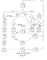
- FIG. 2 when taken together with Figure 11, there is depicted a plurality of basic blocks in flowgraph relation and possible insertion points at the beginning of each block.
- the method inserts only JOIN and ELSE instructions.
- the instruction "JOIN 4" appearing in block B may be replaced by the instruction "DATUM 4". This is because the particular JOIN will never be executed, and all that is needed is the order "4" of the block.
- Figure 3 illustrates one possible execution sequence for the sample program of Figure 2.
- the system embodying the invention provides (1) the use of ELSE and JOIN instructions for enforcing any given priority ordering and (2) the use of any priority ordering in executing multiple paths through the program produced by branch-on-condition instructions. Because in Figure 11, the depicted flowgraph has a large number of possible insertion points, then the issue is to identify a small but sufficient set of insertion points for the ELSE and JOIN instructions in order to enforce a specified order.
- a and B are nodes, then we will use [A, B] to denote the edge from A to B.
- the interval (A, B) is defined as the set of nodes with order greater than that of A and less than that of B.
- the edge [A, B] is increasing if the order of A is less than that of B.
- the edge [A, B] is decreasing if the order of A is greater than that of B.
- B is referred to as the target of edge [A, B].
- An interval is complete, if either no decreasing edge leaves it or all decreasing edges which leave it, leave from the node of maximum order from which no branch returns to the interval.
- An edge corresponding to the failure or success of-a conditional branch likewise corresponds respectively to a left or right branch.
- An interval (A, B) is protected if it can be entered only by an edge from A.
- the preprocessing step involving selective insertion depicted in Figures 2 and 11, is governed by the following criteria:
- condition bits may be set in the counterpart array processor registers.
- Conditional (or unconditonal) branch instructions occur only at the end of a block.
- Condition bits result from the interaction of program and data and represent a control path selection determined by data.
- conditional branch instructions BC
- JOIN JOIN
- ELSE ELSE
- DATUM instructions including unconditional branch instructions capable of being executed on an SIMD machine
- the purpose of the PO register contents is to define priority ordering with reference to inactive processors.
- the IP register is set to the location of the first instruction of the target block.
- argument register 151 interconnects order register plurality 153 to the parallel task processor 41.
- n-priority order registers constituting plurality 153 drive n counterpart activity bit registers 155. These terminate in counterpart ones of n condition CB bit registers 157.
- the complex of argument, order, activity bit and condition registers defines the processing condition of counterpart ones of the parallel processors in array 81.
- Instruction pointer registers 159 are coupled to the instruction processing unit 67 and a target register set 163, 165, and 167 over an address bus 161.
- the register set 163, 165, and 167 modifies the contents of one or more instruction pointer registers.
- the contents of the "0" TGT register are copied into all active instruction pointer registers over bus 161.
- the contents of the "1" TGT register are also copied.
- the contents of the lowest numbered active instruction pointer register are sent over address bus 161 to the IPU as the address of the next instruction to be fetched from the TASK MEMORY 27.
- the scaler processing unit 29 must be altered such that specific registers associated with the pair IPU 67 and LM 69 contain the predetermined values after an instruction FETCH from task memory 27. Accordingly, 0 TGT register 165 contains the address in task memory 27 of the instruction stored immediately after the one currently being executed;
- TGT register 163 contains the address of the instruction to which the control would be transferred if the current instruction were an unconditional branch instruction Cor a conditional branch instruction with conditions satisfied);
- ARG register 151 contains the value of the first operand of the current instruction. Note, that ARG and 1 TGT may be the same register.
- the ELSE instruction which moves control from one basic block to another does this by selectively altering the activity mask. That is, bits in the vector of the activity bit registers are changed.
- the execution of ELSE results in the change of the current block order to be the minimum of the set of block order registers.
- step 1 the instruction ELSE 5 is fetched from memory where it resided at address "d". Alternatively, the instruction may have been prefetched or it may reside in a buffer of the IP U .
- the "0" TG T register receives the address "d"' while the "1" TG T register and the ARG register received the value 5.
- Decoding logic not otherwise illustrated, indicates the following state (1) the instruction is of the ELSE format, and (2) there is no universal agreement. That is, one of the activity registers is 0. Thus, the next step in the execution cycle is step 3. This is followed by steps 10 and 13.
- step 10 referring to Figure 7, both lines 193 and 191 are enabled, and PO registers send their values to the generalized comparator 183. Comparator 183 sends a 1 on its corresponding output line for those PO registers with the minimum value.
- AB 1 will receive a 1, while AB 2 and AB 3 will each receive 0. This yields the final configuration depicted in Figure 3, Subfigure 6.
- Step 3 contemplates two transfers. The first is from ARG register 151 to ORDER registers 153. The second is from "0" TRG register 163 to IP register 159. In step 11, there is a data movement from register 163 to IP registers 159. In contrast, in step 12, the data movement is from companion 1 TGT register 165 to IP register 159.
- control logic includes a plurality of AND gates 1 ,, 171, 173 activating counterpart y registers through switching elements 175, 177, and 179, if the status of the array processor is active, as registered by a 1 in the counterpart activity bit register at the time the AND gates are enabled by an appropriate clocking signal (not shown on path 181).
- Step 10 requires the rewriting of the ACTIVITY bits in register set 155 (Al, A2, An), corresponding to the contents of the order register set 153 made equal to the contents of the ARG register 151.
- Step 10 requires rewriting the contents of the activity bit registers according to the minimum order register contents. This latter is determined by the comparator arrangements 183 and 201 (1)... 201(n).
- FIG. 8 there is shown the logic arrangement for obtaining the next address on bus 161 for an instruction FETCH in parallel task processor 41.
- the address bus 161 is enabled in steps 5, 8, and 13.
- FIGs 9 and 10 there is shown a comparative circuit arrangement for identifying a minimum one of a set of numbers applied to the comparator inputs.
- Note in Figures 9 and 10 at MCOMP (n) compares n values from the n PO registers and gives one value priority order register length in size output and n single bit outputs.
- Figures 9 and 10 further illustrate (a) the relations among the several MCOMP.
Landscapes
- Engineering & Computer Science (AREA)
- Theoretical Computer Science (AREA)
- Software Systems (AREA)
- Physics & Mathematics (AREA)
- General Engineering & Computer Science (AREA)
- General Physics & Mathematics (AREA)
- Computer Hardware Design (AREA)
- Computing Systems (AREA)
- Advance Control (AREA)
- Multi Processors (AREA)
- Complex Calculations (AREA)
- Devices For Executing Special Programs (AREA)
Applications Claiming Priority (2)
| Application Number | Priority Date | Filing Date | Title |
|---|---|---|---|
| US12914880A | 1980-03-10 | 1980-03-10 | |
| US129148 | 1980-03-10 |
Publications (3)
| Publication Number | Publication Date |
|---|---|
| EP0035647A2 true EP0035647A2 (fr) | 1981-09-16 |
| EP0035647A3 EP0035647A3 (en) | 1982-04-28 |
| EP0035647B1 EP0035647B1 (fr) | 1984-10-31 |
Family
ID=22438657
Family Applications (1)
| Application Number | Title | Priority Date | Filing Date |
|---|---|---|---|
| EP81100813A Expired EP0035647B1 (fr) | 1980-03-10 | 1981-02-05 | SIMD-système de traitement des données |
Country Status (3)
| Country | Link |
|---|---|
| EP (1) | EP0035647B1 (fr) |
| JP (1) | JPS56127266A (fr) |
| DE (1) | DE3166883D1 (fr) |
Cited By (23)
| Publication number | Priority date | Publication date | Assignee | Title |
|---|---|---|---|---|
| FR2583904A1 (fr) * | 1985-06-24 | 1986-12-26 | Pixar | Systeme d'ordinateur du type a trains multiples de donnees et instruction unique (simd), avec traitement selectif des donnees |
| EP0223690A2 (fr) | 1985-11-13 | 1987-05-27 | Alcatel N.V. | Réseau de processeurs comportant des moyens de commande de l'état de traitement des cellules |
| WO1987006736A1 (fr) * | 1986-05-01 | 1987-11-05 | The British Petroleum Company P.L.C. | Ameliorations relatives a l'ordre d'execution dans les ordinateurs |
| EP0268342A1 (fr) * | 1986-11-18 | 1988-05-25 | The British Petroleum Company p.l.c. | Coordinateur des éléments de traitement dans un ordinateur à multiprocesseur |
| US4907148A (en) * | 1985-11-13 | 1990-03-06 | Alcatel U.S.A. Corp. | Cellular array processor with individual cell-level data-dependent cell control and multiport input memory |
| WO1993008525A3 (fr) * | 1991-10-24 | 1993-06-24 | Intel Corp | Systeme de traitement de donnees |
| US5361370A (en) * | 1991-10-24 | 1994-11-01 | Intel Corporation | Single-instruction multiple-data processor having dual-ported local memory architecture for simultaneous data transmission on local memory ports and global port |
| US5691920A (en) * | 1995-10-02 | 1997-11-25 | International Business Machines Corporation | Method and system for performance monitoring of dispatch unit efficiency in a processing system |
| US5729726A (en) * | 1995-10-02 | 1998-03-17 | International Business Machines Corporation | Method and system for performance monitoring efficiency of branch unit operation in a processing system |
| US5748855A (en) * | 1995-10-02 | 1998-05-05 | Iinternational Business Machines Corporation | Method and system for performance monitoring of misaligned memory accesses in a processing system |
| US5751945A (en) * | 1995-10-02 | 1998-05-12 | International Business Machines Corporation | Method and system for performance monitoring stalls to identify pipeline bottlenecks and stalls in a processing system |
| US5752062A (en) * | 1995-10-02 | 1998-05-12 | International Business Machines Corporation | Method and system for performance monitoring through monitoring an order of processor events during execution in a processing system |
| US5797019A (en) * | 1995-10-02 | 1998-08-18 | International Business Machines Corporation | Method and system for performance monitoring time lengths of disabled interrupts in a processing system |
| US5949971A (en) * | 1995-10-02 | 1999-09-07 | International Business Machines Corporation | Method and system for performance monitoring through identification of frequency and length of time of execution of serialization instructions in a processing system |
| GB2394815A (en) * | 1999-04-09 | 2004-05-05 | Clearspeed Technology Ltd | Scheduling instruction streams in a SIMD array wherein a determination is made as to which stream has priority and that stream is transferred to the array |
| US7506136B2 (en) | 1999-04-09 | 2009-03-17 | Clearspeed Technology Plc | Parallel data processing apparatus |
| US7526630B2 (en) | 1999-04-09 | 2009-04-28 | Clearspeed Technology, Plc | Parallel data processing apparatus |
| GB2458556A (en) * | 2008-03-24 | 2009-09-30 | Nvidia Corp | Indirect function calls in a synchronous parallel thread processor |
| US7627736B2 (en) | 1999-04-09 | 2009-12-01 | Clearspeed Technology Plc | Thread manager to control an array of processing elements |
| US7802079B2 (en) | 1999-04-09 | 2010-09-21 | Clearspeed Technology Limited | Parallel data processing apparatus |
| US7904698B2 (en) | 2005-02-14 | 2011-03-08 | Koninklijke Philips Electronics N.V. | Electronic parallel processing circuit for performing jump instructions |
| US8171263B2 (en) | 1999-04-09 | 2012-05-01 | Rambus Inc. | Data processing apparatus comprising an array controller for separating an instruction stream processing instructions and data transfer instructions |
| CN109062608A (zh) * | 2012-09-28 | 2018-12-21 | 英特尔公司 | 用于独立数据上递归计算的向量化的读和写掩码更新指令 |
Families Citing this family (3)
| Publication number | Priority date | Publication date | Assignee | Title |
|---|---|---|---|---|
| US4507748A (en) * | 1982-08-02 | 1985-03-26 | International Telephone And Telegraph Corporation | Associative processor with variable length fast multiply capability |
| JPH0654505B2 (ja) * | 1983-12-23 | 1994-07-20 | 株式会社日立製作所 | 並列型演算処理装置 |
| US7856544B2 (en) * | 2008-08-18 | 2010-12-21 | International Business Machines Corporation | Stream processing in super node clusters of processors assigned with stream computation graph kernels and coupled by stream traffic optical links |
Family Cites Families (1)
| Publication number | Priority date | Publication date | Assignee | Title |
|---|---|---|---|---|
| US4149243A (en) * | 1977-10-20 | 1979-04-10 | International Business Machines Corporation | Distributed control architecture with post and wait logic |
-
1981
- 1981-01-27 JP JP975281A patent/JPS56127266A/ja active Granted
- 1981-02-05 DE DE8181100813T patent/DE3166883D1/de not_active Expired
- 1981-02-05 EP EP81100813A patent/EP0035647B1/fr not_active Expired
Cited By (33)
| Publication number | Priority date | Publication date | Assignee | Title |
|---|---|---|---|---|
| FR2583904A1 (fr) * | 1985-06-24 | 1986-12-26 | Pixar | Systeme d'ordinateur du type a trains multiples de donnees et instruction unique (simd), avec traitement selectif des donnees |
| EP0223690A2 (fr) | 1985-11-13 | 1987-05-27 | Alcatel N.V. | Réseau de processeurs comportant des moyens de commande de l'état de traitement des cellules |
| EP0223690A3 (en) * | 1985-11-13 | 1988-07-27 | International Standard Electric Corporation | Processor array with means to control cell processing state |
| US4907148A (en) * | 1985-11-13 | 1990-03-06 | Alcatel U.S.A. Corp. | Cellular array processor with individual cell-level data-dependent cell control and multiport input memory |
| WO1987006736A1 (fr) * | 1986-05-01 | 1987-11-05 | The British Petroleum Company P.L.C. | Ameliorations relatives a l'ordre d'execution dans les ordinateurs |
| EP0244928A1 (fr) * | 1986-05-01 | 1987-11-11 | The British Petroleum Company p.l.c. | Flux de commande dans des ordinateurs |
| EP0268342A1 (fr) * | 1986-11-18 | 1988-05-25 | The British Petroleum Company p.l.c. | Coordinateur des éléments de traitement dans un ordinateur à multiprocesseur |
| WO1988004075A1 (fr) * | 1986-11-18 | 1988-06-02 | The British Petroleum Company P.L.C. | Coordination d'elements processeurs dans un ordinateur multiprocesseur |
| WO1993008525A3 (fr) * | 1991-10-24 | 1993-06-24 | Intel Corp | Systeme de traitement de donnees |
| US5361370A (en) * | 1991-10-24 | 1994-11-01 | Intel Corporation | Single-instruction multiple-data processor having dual-ported local memory architecture for simultaneous data transmission on local memory ports and global port |
| US5517665A (en) * | 1991-10-24 | 1996-05-14 | Intel Corporation | System for controlling arbitration using the memory request signal types generated by the plurality of datapaths having dual-ported local memory architecture for simultaneous data transmission |
| US5530884A (en) * | 1991-10-24 | 1996-06-25 | Intel Corporation | System with plurality of datapaths having dual-ported local memory architecture for converting prefetched variable length data to fixed length decoded data |
| US5752062A (en) * | 1995-10-02 | 1998-05-12 | International Business Machines Corporation | Method and system for performance monitoring through monitoring an order of processor events during execution in a processing system |
| US5729726A (en) * | 1995-10-02 | 1998-03-17 | International Business Machines Corporation | Method and system for performance monitoring efficiency of branch unit operation in a processing system |
| US5748855A (en) * | 1995-10-02 | 1998-05-05 | Iinternational Business Machines Corporation | Method and system for performance monitoring of misaligned memory accesses in a processing system |
| US5751945A (en) * | 1995-10-02 | 1998-05-12 | International Business Machines Corporation | Method and system for performance monitoring stalls to identify pipeline bottlenecks and stalls in a processing system |
| US5691920A (en) * | 1995-10-02 | 1997-11-25 | International Business Machines Corporation | Method and system for performance monitoring of dispatch unit efficiency in a processing system |
| US5797019A (en) * | 1995-10-02 | 1998-08-18 | International Business Machines Corporation | Method and system for performance monitoring time lengths of disabled interrupts in a processing system |
| US5949971A (en) * | 1995-10-02 | 1999-09-07 | International Business Machines Corporation | Method and system for performance monitoring through identification of frequency and length of time of execution of serialization instructions in a processing system |
| US7526630B2 (en) | 1999-04-09 | 2009-04-28 | Clearspeed Technology, Plc | Parallel data processing apparatus |
| US8171263B2 (en) | 1999-04-09 | 2012-05-01 | Rambus Inc. | Data processing apparatus comprising an array controller for separating an instruction stream processing instructions and data transfer instructions |
| GB2394815B (en) * | 1999-04-09 | 2004-08-25 | Clearspeed Technology Ltd | Parallel data processing systems |
| US7506136B2 (en) | 1999-04-09 | 2009-03-17 | Clearspeed Technology Plc | Parallel data processing apparatus |
| GB2394815A (en) * | 1999-04-09 | 2004-05-05 | Clearspeed Technology Ltd | Scheduling instruction streams in a SIMD array wherein a determination is made as to which stream has priority and that stream is transferred to the array |
| GB2348984B (en) * | 1999-04-09 | 2004-05-12 | Pixelfusion Ltd | Parallel data processing systems |
| US7627736B2 (en) | 1999-04-09 | 2009-12-01 | Clearspeed Technology Plc | Thread manager to control an array of processing elements |
| US7802079B2 (en) | 1999-04-09 | 2010-09-21 | Clearspeed Technology Limited | Parallel data processing apparatus |
| US7904698B2 (en) | 2005-02-14 | 2011-03-08 | Koninklijke Philips Electronics N.V. | Electronic parallel processing circuit for performing jump instructions |
| GB2458556B (en) * | 2008-03-24 | 2010-07-07 | Nvidia Corp | Indirect function call instructions in a synchronous parallel thread processor |
| GB2458556A (en) * | 2008-03-24 | 2009-09-30 | Nvidia Corp | Indirect function calls in a synchronous parallel thread processor |
| US8312254B2 (en) | 2008-03-24 | 2012-11-13 | Nvidia Corporation | Indirect function call instructions in a synchronous parallel thread processor |
| CN109062608A (zh) * | 2012-09-28 | 2018-12-21 | 英特尔公司 | 用于独立数据上递归计算的向量化的读和写掩码更新指令 |
| CN109062608B (zh) * | 2012-09-28 | 2023-09-22 | 英特尔公司 | 用于独立数据上递归计算的向量化的读和写掩码更新指令 |
Also Published As
| Publication number | Publication date |
|---|---|
| JPS56127266A (en) | 1981-10-05 |
| EP0035647A3 (en) | 1982-04-28 |
| EP0035647B1 (fr) | 1984-10-31 |
| DE3166883D1 (en) | 1984-12-06 |
| JPS6155707B2 (fr) | 1986-11-28 |
Similar Documents
| Publication | Publication Date | Title |
|---|---|---|
| EP0035647A2 (fr) | SIMD-système de traitement des données | |
| US4435758A (en) | Method for conditional branch execution in SIMD vector processors | |
| EP0231928B1 (fr) | Circuit pour la commande par programme | |
| EP0219203B1 (fr) | Commande de calculateur avec branchement en un cycle | |
| US5710902A (en) | Instruction dependency chain indentifier | |
| US7853779B2 (en) | Methods and apparatus for scalable array processor interrupt detection and response | |
| US5487159A (en) | System for processing shift, mask, and merge operations in one instruction | |
| US4740893A (en) | Method for reducing the time for switching between programs | |
| US7509480B2 (en) | Selection of ISA decoding mode for plural instruction sets based upon instruction address | |
| JP3771273B2 (ja) | 述語レジスタ・セットをレストアする方法および装置 | |
| US4991078A (en) | Apparatus and method for a pipelined central processing unit in a data processing system | |
| US6681341B1 (en) | Processor isolation method for integrated multi-processor systems | |
| EP0307166A2 (fr) | Processeur de données | |
| US3983541A (en) | Polymorphic programmable units employing plural levels of phased sub-instruction sets | |
| US4558411A (en) | Polymorphic programmable units employing plural levels of sub-instruction sets | |
| KR19990062575A (ko) | N-지로 분기를 갖는 슈퍼스칼라 또는 초장 명령어 워드컴퓨터에서 다음 명령어를 선택하는 방법 및 장치 | |
| EA004196B1 (ru) | Управляющий программный продукт и система обработки данных | |
| US4045782A (en) | Microprogrammed processor system having external memory | |
| EP0354585B1 (fr) | Microprocesseur à pipeline d'instructions | |
| EP0032515B1 (fr) | Procede de commande de pipeline pour un ordinateur | |
| KR100777772B1 (ko) | 연산 처리 장치, 정보 처리 장치 및 레지스터 파일의 제어방법 | |
| EP0164418B1 (fr) | Systeme de commande par microprogramme | |
| US5479620A (en) | Control unit modifying micro instructions for one cycle execution | |
| EP0660229B1 (fr) | Méthode et dispositif pour modifier le contenu d'un registre | |
| EP0448317B1 (fr) | Appareil de traitement de données de longueur variable |
Legal Events
| Date | Code | Title | Description |
|---|---|---|---|
| PUAI | Public reference made under article 153(3) epc to a published international application that has entered the european phase |
Free format text: ORIGINAL CODE: 0009012 |
|
| AK | Designated contracting states |
Designated state(s): DE FR GB IT |
|
| PUAL | Search report despatched |
Free format text: ORIGINAL CODE: 0009013 |
|
| AK | Designated contracting states |
Designated state(s): DE FR GB IT |
|
| 17P | Request for examination filed |
Effective date: 19820519 |
|
| GRAA | (expected) grant |
Free format text: ORIGINAL CODE: 0009210 |
|
| AK | Designated contracting states |
Designated state(s): DE FR GB IT |
|
| PG25 | Lapsed in a contracting state [announced via postgrant information from national office to epo] |
Ref country code: IT Free format text: LAPSE BECAUSE OF FAILURE TO SUBMIT A TRANSLATION OF THE DESCRIPTION OR TO PAY THE FEE WITHIN THE PRESCRIBED TIME-LIMIT;WARNING: LAPSES OF ITALIAN PATENTS WITH EFFECTIVE DATE BEFORE 2007 MAY HAVE OCCURRED AT ANY TIME BEFORE 2007. THE CORRECT EFFECTIVE DATE MAY BE DIFFERENT FROM THE ONE RECORDED. Effective date: 19841031 |
|
| REF | Corresponds to: |
Ref document number: 3166883 Country of ref document: DE Date of ref document: 19841206 |
|
| ET | Fr: translation filed | ||
| PLBE | No opposition filed within time limit |
Free format text: ORIGINAL CODE: 0009261 |
|
| STAA | Information on the status of an ep patent application or granted ep patent |
Free format text: STATUS: NO OPPOSITION FILED WITHIN TIME LIMIT |
|
| 26N | No opposition filed | ||
| PGFP | Annual fee paid to national office [announced via postgrant information from national office to epo] |
Ref country code: GB Payment date: 19920113 Year of fee payment: 12 |
|
| PGFP | Annual fee paid to national office [announced via postgrant information from national office to epo] |
Ref country code: FR Payment date: 19920124 Year of fee payment: 12 |
|
| PGFP | Annual fee paid to national office [announced via postgrant information from national office to epo] |
Ref country code: DE Payment date: 19920304 Year of fee payment: 12 |
|
| PG25 | Lapsed in a contracting state [announced via postgrant information from national office to epo] |
Ref country code: GB Effective date: 19930205 |
|
| GBPC | Gb: european patent ceased through non-payment of renewal fee |
Effective date: 19930205 |
|
| PG25 | Lapsed in a contracting state [announced via postgrant information from national office to epo] |
Ref country code: FR Effective date: 19931029 |
|
| PG25 | Lapsed in a contracting state [announced via postgrant information from national office to epo] |
Ref country code: DE Effective date: 19931103 |
|
| REG | Reference to a national code |
Ref country code: FR Ref legal event code: ST |