EP0035710B1 - Circuit de réglage de courant continu - Google Patents
Circuit de réglage de courant continu Download PDFInfo
- Publication number
- EP0035710B1 EP0035710B1 EP81101417A EP81101417A EP0035710B1 EP 0035710 B1 EP0035710 B1 EP 0035710B1 EP 81101417 A EP81101417 A EP 81101417A EP 81101417 A EP81101417 A EP 81101417A EP 0035710 B1 EP0035710 B1 EP 0035710B1
- Authority
- EP
- European Patent Office
- Prior art keywords
- valve
- load
- swinging
- gate device
- capacitor
- Prior art date
- Legal status (The legal status is an assumption and is not a legal conclusion. Google has not performed a legal analysis and makes no representation as to the accuracy of the status listed.)
- Expired
Links
- 239000003990 capacitor Substances 0.000 claims abstract description 45
- 230000003534 oscillatory effect Effects 0.000 claims 3
- 230000010355 oscillation Effects 0.000 description 8
- 238000010791 quenching Methods 0.000 description 6
- 230000000171 quenching effect Effects 0.000 description 5
- 238000000034 method Methods 0.000 description 4
- 230000008033 biological extinction Effects 0.000 description 3
- 238000011144 upstream manufacturing Methods 0.000 description 3
- 238000013016 damping Methods 0.000 description 2
- 238000010304 firing Methods 0.000 description 2
- 230000001681 protective effect Effects 0.000 description 2
- 230000003111 delayed effect Effects 0.000 description 1
- 230000001419 dependent effect Effects 0.000 description 1
- 238000009499 grossing Methods 0.000 description 1
- 239000000463 material Substances 0.000 description 1
- 238000001208 nuclear magnetic resonance pulse sequence Methods 0.000 description 1
- 230000002441 reversible effect Effects 0.000 description 1
- 238000004904 shortening Methods 0.000 description 1
Images
Classifications
-
- H—ELECTRICITY
- H02—GENERATION; CONVERSION OR DISTRIBUTION OF ELECTRIC POWER
- H02M—APPARATUS FOR CONVERSION BETWEEN AC AND AC, BETWEEN AC AND DC, OR BETWEEN DC AND DC, AND FOR USE WITH MAINS OR SIMILAR POWER SUPPLY SYSTEMS; CONVERSION OF DC OR AC INPUT POWER INTO SURGE OUTPUT POWER; CONTROL OR REGULATION THEREOF
- H02M3/00—Conversion of DC power input into DC power output
- H02M3/02—Conversion of DC power input into DC power output without intermediate conversion into AC
- H02M3/04—Conversion of DC power input into DC power output without intermediate conversion into AC by static converters
- H02M3/10—Conversion of DC power input into DC power output without intermediate conversion into AC by static converters using discharge tubes with control electrode or semiconductor devices with control electrode
- H02M3/125—Conversion of DC power input into DC power output without intermediate conversion into AC by static converters using discharge tubes with control electrode or semiconductor devices with control electrode using devices of a thyratron or thyristor type requiring extinguishing means
- H02M3/135—Conversion of DC power input into DC power output without intermediate conversion into AC by static converters using discharge tubes with control electrode or semiconductor devices with control electrode using devices of a thyratron or thyristor type requiring extinguishing means using semiconductor devices only
Definitions
- the invention relates to a DC control circuit with the features listed in the preamble of claim 1.
- a DC regulator circuit is known from German Offenlegungsschrift 2622351.
- the voltage of a given DC voltage source can be reduced in such a way that the mean value of the input voltage for a connected load can be controlled down to almost zero.
- This average is primarily dependent on the duty cycle of the main valve. Due to the necessary swinging of the charge of the commutation capacitor, the minimum switch-on times of the main valve cannot be fallen below.
- the voltage of the commutation capacitor is applied to the load in addition to the input voltage.
- the commutation capacitor In the normal control range, the commutation capacitor is left in the polarity between the extinction and re-ignition of the main valve, which polarity it has assumed due to the current commutated on the extinguishing branch during the extinguishing process.
- This state of the commutation capacitor is maintained even after the main valve has been ignited and only at a point in time coordinated with the dimensions of the swinging choke and the commutation capacitor before the intended ignition of the commutation valve (quenching valve) is the polarity of the capacitor reversed by firing the reversing valve and the circuit for quenching the main valve prepared.
- the extinguishing valve and the return valve are ignited simultaneously.
- the duty cycle of the main valve is reduced by shortening the time interval between the ignition times of the main valve and the reversing valve until both ignition times coincide.
- the main valve no longer receives any ignition pulses.
- the output voltage arises from the fact that in the time interval between the ignition of the return valve and the end of the return process (extinction of the return valve) the commutation valve is energized and thus a superposition of the voltage of the DC voltage source and the voltage on the commutation capacitor is applied to the load.
- the reduction in the output voltage thus occurs in that the ignition timing for the commutation valve, which is to be placed in the current carrying time of the return valve (which can also be a diode), is delayed and is shifted to the extinction time of the return valve. This reduces the section of the capacitor voltage to be placed on the load.
- the invention has for its object to provide a DC chopper, the output voltage is extended over the range that can be achieved by controlling the main valve duty cycle and in which an overload of the commutation capacitor is kept low without using a recharging branch.
- a common inductance can be used as a return choke and a changeover choke, which is connected upstream of an anti-parallel connection of the changeover valve and the return valve.
- This inductance and the commutation capacitor thus form a resonant circuit for swinging around and swinging back, in which the swinging back valve and the swinging around valve lie.
- this inductance is divided into two parts, one part being formed by a further choke which is arranged in the connecting line between the commutation capacitor and the one terminal of the load.
- the two free-wheeling diodes connect the two choke ends to the connecting line coming from the other load connection, so that this part of the resonant circuit inductance is short-circuited in operating states in which both free-wheeling diodes are conductive at the same time.
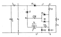
- the terminals 1 of a DC voltage source, their inductance 2 and their capacitance 3 are shown symbolically: In particular, this can be a DC voltage supply network with a downstream input inductance and a smoothing capacitor.
- the consumer is symbolized by an inductor 4 with an ohmic component 5.
- the input terminal 6 is connected via a line 7 to one pole of the DC voltage source, the other load input 8 via a line 9 to the other pole of the DC voltage source.
- line 7 is the controllable main valve of the DC controller circuit, which is designed as a thyristor HT.
- the two connections of the main valve HT are through an extinguishing branch. connected with each other.
- the extinguishing branch consists of a controllable commutation valve which is poled parallel to the main valve and which serves as an extinguishing valve in the normal control range and is also designed as a thyristor LT.
- a commutation capacitor C is connected downstream of this commutation valve LT.
- One electrode of the commutation valve LT is therefore connected to an output of the DC voltage source together with an electrode of the main valve HT, the other electrode of the commutation valve LT is connected via capacitor C to the other electrode of the main valve and the load input 6.
- a swinging branch Parallel to the commutation capacitor is a swinging branch which is formed from a controllable swinging valve (swinging thyristor UT) and a swinging choke.
- This swing branch is in series with the combutation valve LT, ie it leads from the connection point between LT and C to the load input 6.
- the swing valve UT is polarized in the direction of current flow of the commutation valve LT.
- a return oscillation branch which contains a return oscillation valve with an upstream return oscillation choke which is polarized opposite to the direction of current flow of the commutation valve.
- the return valve can be a thyristor, but it can also be designed as a return diode RD. It is advantageous to use only one common throttle Lsw as the oscillating choke and swinging choke; In this case, the valves UT and RD are connected in anti-parallel and are located in series with the throttle L sw in the connecting line between points 10 and 6.
- a first freewheel valve (diode FD1) is arranged parallel to the load 4, 5.
- the arrangement of these components corresponds to the known circuits, but a reloading branch corresponding to the known arrangements is dispensed with.
- the arrangement can be supplemented by a protective inductance L LS for the valves HT and FD1 if the input inductance 2 is not sufficient for this. Care must be taken to ensure that this protective inductance lies outside the current path which is formed by the elements 2, LT, C, FD2 and the line 9.
- the circuit is supplemented by a further choke L ss , which is connected downstream of the connection of the commutation capacitor C leading to the load input 6 within the part of the quenching arm which is parallel to the resonant circuit, and by a second free-wheeling valve which connects the voltage source 1 to the other load input 8 leading connecting line with the load-side connection of the commutation capacitor C connects.
- This second one-way valve FD2 is poled in parallel to the first one-way valve FD1. If both valves are live, they release a line for bridging the other throttle L ss .
- the energy originally stored in the capacitor C is stored in the inductance in order to be fed back into the capacitor during the oscillation.
- the voltage returns to its original value after a sinusoidal oscillation. If the commutation valve LT is now ignited during this oscillation, the oscillating circuit is connected to the voltage of the voltage source until the free-wheeling valve FD1 extinguishes and thus there is a short-term increase in current through the commutation capacitor C.
- the oscillating circuit energy is thus increased briefly when LT is ignited. After the end of the swing back, the capacitor is therefore charged more than before the start of the swing.
- the capacitor voltage thus increases with each ignition pulse and is ultimately only limited by the ohmic resistances of the circuit. However, these should be kept low with a view to high efficiency.
- the FD2 cathode becomes negative with respect to the FD1 cathode, so that FD1 blocks and FD2 takes over the load current.
- the current commutates from FD2 to FD1.
- This commutation is relatively slow, so that Lss is short-circuited for a while and the resonant circuit inductance is only formed by L sw .
- the capacitor voltage also rises more slowly, which corresponds to a reduction in the energy in the resonant circuit.
- This energy reduction is caused by the fact that the energy to be dissipated is stored outside the resonant circuit, namely in the inductance L ss , without ohmic losses occurring. It can be achieved by optimizing the throttle dimensions that just as much energy is withdrawn from the resonant circuit as is supplied after the commutation valve has been ignited. This results in a minimal capacitor overload where J A is the load current. This overload was only 10% of the DC input voltage in a first laboratory system, while it was 60% in a same system without a second freewheeling diode. Furthermore, most valves are stressed less because of the voltage division at the chokes L sw and Lss. The quenching voltage peak in the output voltage is also reduced, by 50% in the aforementioned laboratory system. The consequence of this is that not only can a reloading branch be dispensed with, but the other components can also be designed for a lower maximum load.
- the optimal division of the resonant circuit inductance into the inductances L ss and L sw results from a consideration of the resonant circuit.
- the resonant circuit damping can be detected by parameter h, which represents the ratio of the capacitor voltage 0 before ignition of the return valve to the capacitor voltage U i8o ° after half the period of oscillation .
Landscapes
- Engineering & Computer Science (AREA)
- Power Engineering (AREA)
- Dc-Dc Converters (AREA)
- Lock And Its Accessories (AREA)
- Ignition Installations For Internal Combustion Engines (AREA)
- Power Conversion In General (AREA)
- Control Of Electrical Variables (AREA)
Claims (2)
caractérisé par


Priority Applications (1)
| Application Number | Priority Date | Filing Date | Title |
|---|---|---|---|
| AT81101417T ATE6111T1 (de) | 1980-03-07 | 1981-02-26 | Gleichstromstellerschaltung. |
Applications Claiming Priority (2)
| Application Number | Priority Date | Filing Date | Title |
|---|---|---|---|
| DE3008907 | 1980-03-07 | ||
| DE19803008907 DE3008907A1 (de) | 1980-03-07 | 1980-03-07 | Gleichstromstellerschaltung |
Publications (3)
| Publication Number | Publication Date |
|---|---|
| EP0035710A2 EP0035710A2 (fr) | 1981-09-16 |
| EP0035710A3 EP0035710A3 (en) | 1982-03-03 |
| EP0035710B1 true EP0035710B1 (fr) | 1984-02-01 |
Family
ID=6096597
Family Applications (1)
| Application Number | Title | Priority Date | Filing Date |
|---|---|---|---|
| EP81101417A Expired EP0035710B1 (fr) | 1980-03-07 | 1981-02-26 | Circuit de réglage de courant continu |
Country Status (5)
| Country | Link |
|---|---|
| US (1) | US4358811A (fr) |
| EP (1) | EP0035710B1 (fr) |
| JP (1) | JPS56139076A (fr) |
| AT (1) | ATE6111T1 (fr) |
| DE (2) | DE3008907A1 (fr) |
Families Citing this family (4)
| Publication number | Priority date | Publication date | Assignee | Title |
|---|---|---|---|---|
| US4394724A (en) * | 1981-10-30 | 1983-07-19 | Westinghouse Electric Corp. | Propulsion motor control apparatus and method |
| GB8402629D0 (en) * | 1984-02-01 | 1984-03-07 | Mcewan P M | Circuit breakers |
| ES2071730T3 (es) * | 1990-12-10 | 1995-07-01 | Asea Brown Boveri | Procedimiento y dispositivo para la eliminacion o reduccion de armonicas y/o de oscilaciones de resonancia. |
| EP0489947B1 (fr) * | 1990-12-10 | 1995-03-22 | Asea Brown Boveri Ag | Circuit d'extinction |
Family Cites Families (6)
| Publication number | Priority date | Publication date | Assignee | Title |
|---|---|---|---|---|
| US3414797A (en) * | 1966-05-20 | 1968-12-03 | Gen Electric | Power converter employing integrated magnetics |
| GB1239734A (fr) * | 1969-01-13 | 1971-07-21 | ||
| BE775787A (fr) * | 1971-11-25 | 1972-05-25 | Acec | Dispositif electronique de reglage d'un courant continu. |
| FR2320658A1 (fr) * | 1975-08-07 | 1977-03-04 | Jeumont Schneider | Perfectionnement aux hacheurs de courant a frequence constante susceptibles d'alimenter a faible debit une charge inductive |
| FR2345760A1 (fr) * | 1976-03-26 | 1977-10-21 | Cem Oerlikon Traction | Dispositif regleur de courant continu |
| DE2831752A1 (de) * | 1978-07-19 | 1980-01-31 | Siemens Ag | Umrichter mit einem gleichspannungszwischenkreis |
-
1980
- 1980-03-07 DE DE19803008907 patent/DE3008907A1/de not_active Withdrawn
-
1981
- 1981-02-26 EP EP81101417A patent/EP0035710B1/fr not_active Expired
- 1981-02-26 AT AT81101417T patent/ATE6111T1/de not_active IP Right Cessation
- 1981-02-26 DE DE8181101417T patent/DE3162073D1/de not_active Expired
- 1981-03-03 US US06/239,977 patent/US4358811A/en not_active Expired - Fee Related
- 1981-03-06 JP JP3236081A patent/JPS56139076A/ja active Pending
Also Published As
| Publication number | Publication date |
|---|---|
| DE3008907A1 (de) | 1981-09-17 |
| ATE6111T1 (de) | 1984-02-15 |
| US4358811A (en) | 1982-11-09 |
| EP0035710A3 (en) | 1982-03-03 |
| JPS56139076A (en) | 1981-10-30 |
| EP0035710A2 (fr) | 1981-09-16 |
| DE3162073D1 (en) | 1984-03-08 |
Similar Documents
| Publication | Publication Date | Title |
|---|---|---|
| DE69803521T2 (de) | Verfahren und apparat zur unterdrückung reflektierter energie aufgrund von stufenfehlanpassung in einem nichtlinearen magnetischen kompressionsmodul | |
| DE3734989A1 (de) | Gleichstromleitungsunterbrecher und verfahren zu dessen kommutierung | |
| DE102006029475A1 (de) | Effiziente Einschaltstrom-Begrenzungsschaltung mit bidirektionellen Doppelgate-HEMT-Bauteilen | |
| DE2320128C3 (de) | Zerhacker | |
| DE2936063A1 (de) | Dimmerschaltkreis | |
| DE1763411C3 (de) | Thyristor-Stromrichteranordnung | |
| DE2639944A1 (de) | Gleichspannungswandler | |
| DE4421249C2 (de) | Schaltstromversorgungsgerät mit Snubber-Schaltung | |
| DE2644715C2 (de) | Einrichtung zur Befreiung elektrischer oder elektronischer Einwegschalter von hoher Verlustleistungsbeanspruchung während des Einschaltens - bei welchem ein, zuvor in einem anderen Schaltungspfad fließender, von Null verschiedener Strom auf den betreffenden Einwegschalter überwechselt - und von überhöhter Sperrspannungsbeanspruchung zum Ende des Ausschaltens | |
| DE2357925A1 (de) | Schaltung zur begrenzung des ladestromanstiegs | |
| DE3405793A1 (de) | Verfahren und vorrichtung zum kurzschlussschutz eines stromrichtergeraetes mit gto-thyristoren | |
| EP2992598A1 (fr) | Convertisseur élévateur ou abaisseur à condensateur de décharge | |
| DE2348952B2 (de) | Kommutierungseinrichtung fuer eine gleichstrom-zerhackerschaltung | |
| DE1638311A1 (de) | Stromkreis mit steuerbaren Gleichrichtern | |
| EP0035710A2 (fr) | Circuit de réglage de courant continu | |
| EP0009225B1 (fr) | Circuit de protection | |
| DE1638962A1 (de) | Stromkreis mit steuerbaren Gleichrichtern | |
| DE2716367C2 (de) | Schutzbeschaltung für im Wechselschaltbetrieb gegen induktive Last arbeitende Transistoren | |
| DE2632785C3 (de) | Gleichstromzerhacker | |
| DE2541687C3 (de) | Umrichter und Verfahren zu seinem Betrieb | |
| DE3612524C2 (fr) | ||
| DE3049020C2 (de) | Regelbarer Gleichspannungswandler für Leistungsschaltnetzteile | |
| DE3717488C2 (fr) | ||
| DE69007761T2 (de) | Schaltungsanordnung für Stromversorgung einer Last wie Magnetron. | |
| EP0539902A2 (fr) | Circuit électrique de dégagement au blocage pour un convertisseur de tension continu |
Legal Events
| Date | Code | Title | Description |
|---|---|---|---|
| PUAI | Public reference made under article 153(3) epc to a published international application that has entered the european phase |
Free format text: ORIGINAL CODE: 0009012 |
|
| AK | Designated contracting states |
Designated state(s): AT CH DE |
|
| PUAL | Search report despatched |
Free format text: ORIGINAL CODE: 0009013 |
|
| 17P | Request for examination filed |
Effective date: 19811028 |
|
| AK | Designated contracting states |
Designated state(s): AT CH DE |
|
| GRAA | (expected) grant |
Free format text: ORIGINAL CODE: 0009210 |
|
| AK | Designated contracting states |
Designated state(s): AT CH DE LI |
|
| REF | Corresponds to: |
Ref document number: 6111 Country of ref document: AT Date of ref document: 19840215 Kind code of ref document: T |
|
| REF | Corresponds to: |
Ref document number: 3162073 Country of ref document: DE Date of ref document: 19840308 |
|
| PGFP | Annual fee paid to national office [announced via postgrant information from national office to epo] |
Ref country code: DE Payment date: 19840329 Year of fee payment: 4 |
|
| PGFP | Annual fee paid to national office [announced via postgrant information from national office to epo] |
Ref country code: CH Payment date: 19840524 Year of fee payment: 4 |
|
| PLBE | No opposition filed within time limit |
Free format text: ORIGINAL CODE: 0009261 |
|
| STAA | Information on the status of an ep patent application or granted ep patent |
Free format text: STATUS: NO OPPOSITION FILED WITHIN TIME LIMIT |
|
| 26N | No opposition filed | ||
| PGFP | Annual fee paid to national office [announced via postgrant information from national office to epo] |
Ref country code: AT Payment date: 19870128 Year of fee payment: 7 |
|
| PG25 | Lapsed in a contracting state [announced via postgrant information from national office to epo] |
Ref country code: AT Effective date: 19890226 |
|
| PG25 | Lapsed in a contracting state [announced via postgrant information from national office to epo] |
Ref country code: LI Effective date: 19890228 Ref country code: CH Effective date: 19890228 |
|
| REG | Reference to a national code |
Ref country code: CH Ref legal event code: PL |
|
| PG25 | Lapsed in a contracting state [announced via postgrant information from national office to epo] |
Ref country code: DE Effective date: 19891101 |