EP0035767A1 - Dispositif semiconducteur - Google Patents
Dispositif semiconducteur Download PDFInfo
- Publication number
- EP0035767A1 EP0035767A1 EP81101619A EP81101619A EP0035767A1 EP 0035767 A1 EP0035767 A1 EP 0035767A1 EP 81101619 A EP81101619 A EP 81101619A EP 81101619 A EP81101619 A EP 81101619A EP 0035767 A1 EP0035767 A1 EP 0035767A1
- Authority
- EP
- European Patent Office
- Prior art keywords
- semiconductor
- control element
- component
- current
- monitoring
- Prior art date
- Legal status (The legal status is an assumption and is not a legal conclusion. Google has not performed a legal analysis and makes no representation as to the accuracy of the status listed.)
- Granted
Links
Images
Classifications
-
- H—ELECTRICITY
- H10—SEMICONDUCTOR DEVICES; ELECTRIC SOLID-STATE DEVICES NOT OTHERWISE PROVIDED FOR
- H10W—GENERIC PACKAGES, INTERCONNECTIONS, CONNECTORS OR OTHER CONSTRUCTIONAL DETAILS OF DEVICES COVERED BY CLASS H10
- H10W42/00—Arrangements for protection of devices
-
- H—ELECTRICITY
- H02—GENERATION; CONVERSION OR DISTRIBUTION OF ELECTRIC POWER
- H02H—EMERGENCY PROTECTIVE CIRCUIT ARRANGEMENTS
- H02H7/00—Emergency protective circuit arrangements specially adapted for specific types of electric machines or apparatus or for sectionalised protection of cable or line systems, and effecting automatic switching in the event of an undesired change from normal working conditions
- H02H7/20—Emergency protective circuit arrangements specially adapted for specific types of electric machines or apparatus or for sectionalised protection of cable or line systems, and effecting automatic switching in the event of an undesired change from normal working conditions for electronic equipment
- H02H7/205—Emergency protective circuit arrangements specially adapted for specific types of electric machines or apparatus or for sectionalised protection of cable or line systems, and effecting automatic switching in the event of an undesired change from normal working conditions for electronic equipment for controlled semi-conductors which are not included in a specific circuit arrangement
-
- H—ELECTRICITY
- H03—ELECTRONIC CIRCUITRY
- H03K—PULSE TECHNIQUE
- H03K17/00—Electronic switching or gating, i.e. not by contact-making and –breaking
- H03K17/08—Modifications for protecting switching circuit against overcurrent or overvoltage
- H03K17/082—Modifications for protecting switching circuit against overcurrent or overvoltage by feedback from the output to the control circuit
- H03K17/0826—Modifications for protecting switching circuit against overcurrent or overvoltage by feedback from the output to the control circuit in bipolar transistor switches
-
- H—ELECTRICITY
- H03—ELECTRONIC CIRCUITRY
- H03K—PULSE TECHNIQUE
- H03K17/00—Electronic switching or gating, i.e. not by contact-making and –breaking
- H03K17/08—Modifications for protecting switching circuit against overcurrent or overvoltage
- H03K2017/0806—Modifications for protecting switching circuit against overcurrent or overvoltage against excessive temperature
Definitions
- the invention relates to a semiconductor arrangement with at least one semiconductor component and with a control element monitoring its function.
- the operating parameters in particular the load current and the temperature, must be monitored.
- bimetallic switches or PPC resistors or NTC resistors are used as thermal sensors, which are attached to the semiconductor component and cause the latter to be switched off when the maximum permissible operating temperature of the latter is reached.
- control elements cannot be attached directly to the semiconductor body of the components. As a result of the thermal resistances present between the semiconductor body and the control element, there is a delay in response, which often prevents effective protection of the semiconductor components by such thermal sensors.
- the invention was therefore based on the object of specifying a monitoring device for semiconductor components which in any case enables the electrical or thermal operating behavior of semiconductor components to be checked reliably and as quickly as possible.
- the invention is based on the knowledge that when current flows through a semiconductor body, so-called recombination radiation arises, that this radiation is infrared radiation, and that this infrared radiation is proportional to the current flow.
- the control element is provided at the same time for monitoring the load current and the temperature of the semiconductor component.
- transition pn control elements based on semiconductors both with transition pn least one, and for temperature monitoring with the aid of their D urchlledge s or with the aid of its dark-current behavior, or control elements on semiconductor basis without and for temperature monitoring with the aid of its dark resistance change in each case in the blocking phase of the semiconductor component, be provided.
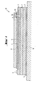
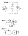
- the subject matter of the invention is shown and explained on the basis of the exemplary embodiments illustrated in FIGS. 1-4.
- FIG. 1 shows in cross section the semiconductor body of a thyristor to be monitored with a control element directly attached to it.
- FIG. 2 schematically shows the semiconductor arrangement according to the invention and a circuit arrangement suitable for evaluating the function of the control element.
- FIG. 3 shows partly in cross section and partly in side view the structure of a semiconductor component with parts of its housing and with a control element thermally attached to the housing.
- FIG. 4 schematically shows a photoresistor connected to a monitoring circuit, which is to be fastened in a corresponding manner to a semiconductor component.
- the semiconductor body 10 according to FIG. 1 forming a thyristor structure consists of a high-resistance, n-conducting central zone 1, of a higher-doped p-conducting zone 2 or 3 adjacent to each side thereof, and of a highly doped, n introduced into the upper zone conductive zone 5, and from the outer zones 2 and 5 applied contact electrodes 4 and 7 for the load current connection and from the p-conductive zone 3 applied control electrode 6 for the control connection.
- This layer structure is fixed between conductor parts 15 and 17.
- the semiconductor body 10 has an opening 8 which extends from a surface, for example from the contact electrode 7, into the p-type zone 3 and serves as a radiation window for the recombination radiation which arises in the semiconductor body when current flows. Because of the tendency of highly doped semiconductor material to absorb the recombination radiation, it is not sufficient to only to expose the semiconductor surface for producing a radiation surface, but an opening with a depth into one of the higher-resistance zones is required.
- the cross section of the opening 8 is adapted to the exposure surface of the control element provided.
- the position of the opening 8 is essentially arbitrary. For technological reasons, however, it is preferably located on the edge of the area determined by the contact electrode 7, for example in a cutout in the current conductor 17. In principle, the recombination radiation must emerge from the semiconductor material and strike the surface of the control element to be exposed. Accordingly, the control element with the surface section provided for the exposure is also attached in a corresponding manner to the semiconductor body.
- the control element is attached to the correspondingly prepared surface section of the semiconductor body 10 via an electrically insulating layer 20.
- Both the insulating material body 20 and the control element 30 can be attached, for example, by gluing or by soldering.
- an insulating body e.g. serve an adapted annular disc made of oxide ceramic, which is connected at its surfaces to the adjacent components and has a recess in its central area for the passage of the radiation onto the surface of the monitoring element to be exposed.
- a disk made of quartz can also be provided as the insulating material body 20, since quartz is completely permeable to the recombination radiation.
- Another possibility is to provide a corresponding socket for the arrangement of the control element 30, . Which can be attached to the insulating body 20 in the desired manner, and in which the control element is held.
- the entire exposed surface of the opening 8 can be provided with a layer of the oxide of the semiconductor material as a protective coating.
- the opening 8 can be produced by etching or by other known ablation processes.
- the control element 30 is thermally coupled to the semiconductor body 10 as described. This optimally allows both the current monitoring in the semiconductor component and the monitoring of the operating temperature thereof, which can increase undesirably, for example, due to failure of the cooling of the semiconductor component or due to deterioration in heat transfer in the structure of the latter.
- control elements without a pn junction, i.e. so-called photoresistors, and those based on semiconductors with at least one pn junction, i.e. Photodiodes and phototransistors are provided.
- the recombination radiation in the semiconductor body is proportional to the current flow through it over a wide range.
- the invention advantageously makes use of this fact, as well as the fact that control elements with a pn junction, the transmission behavior thereof and their dark current and, in the case of photoresistors, their dark resistance can be related to the operating temperature of the control element and thus also of the semiconductor component to be monitored.
- it is surprisingly easy to achieve essentially performance-free, inertia-free and phase-accurate monitoring of parameters in semiconductor components.
- a photodiode 30 is connected via a switch 31 on the one hand to a measuring circuit 32 for determining the forward voltage drop of the photodiode and on the other hand to a measuring circuit 33 for measuring the photocurrent.
- the switch can preferably be switched over with the help of a grid-synchronous clock generator in time with the grid frequency half-waves.
- a constant forward current of the latter is impressed by a current generator in the measuring circuit 32 of the photodiode 30, and the forward voltage drop of the photodiode is determined as a function of the thermal coupling of the photodiode to the component to be protected. This changes inversely proportional to the ambient temperature, so that a direct comparison of the measured values with the operating temperature to be monitored is possible.
- the photodiode 30 is acted on in the reverse direction with the aid of a voltage source in the measuring circuit 33, and the photocurrent is represented as a function of the illuminance on the exposed surface of the control element.
- the circuits as such. And the measures for measuring electrical quantities of the control element 30 and if necessary to reinforce the same are well known and not the subject of the invention.
- the dark current can also be represented as a function of the ambient temperature, it is possible to carry out temperature monitoring with the aid of the dark current in view of the usability of the control elements provided, even at high frequencies.
- a suitable error message can also be connected, for example, and a signal for an ignition lock can also be given for the ignition circuit of the component to be monitored, if it is a thyristor.
- the measurement results can thus be evaluated in a manner known per se and known from electronics.
- the block circuit shown in Figure 2 is not limited to the connection with only one control element. Rather, for a semiconductor rectifier circuit with six rectifier components, for example, all six control elements can be connected to the monitoring circuit shown.
- FIG. 1 Another possibility for the attachment of a control element is shown in FIG.
- the latter is provided with an opening 8.
- the control element 30 is attached via an insulating body 20 to a holding device 15 a in such a way that the recombination radiation emerging from the opening 8 of the semiconductor body 10 hits the surface of each control element to be exposed. It goes without saying that the assembly of such an arrangement requires special identifications of the housing parts for their position of certain mutual spatial assignment to ensure the functionality of the control element.
- the bracket 15 a is preferably made of a good heat-conducting metal for optimal thermal coupling of the control element to the housing 15 and is mounted so that the control element is as close as possible to the semiconductor body 10.
- control element 30 can also be attached at a suitable location on the base body 24.
- the connecting lines of the control element can be inserted through the housing at the top, for example with the aid of a ceramic tube.
- a photoresistor 30 is exposed to radiation of the semiconductor body, which is indicated only by arrows.
- the so-called light resistance of the control element 30 is a function of the illuminance.
- a base voltage is impressed on the photoresistor 30 from a battery 35 in the base circuit.
- the photocurrent generated by radiation in the photoresistor produces a change in resistance, which is evaluated with the aid of the voltage drop across the measuring resistor 36 and the circuit 37, which is not essential to the invention, which is connected in parallel with this.
- the dark resistance of the control element 30 can also serve as a function of the operating temperature of the latter and that of the semiconductor component for monitoring it.
- the semiconductor body 10 is first attached in a manner known per se to the pretreated carrier body 24 and the upper connecting conductor thereon, only a part of which is indicated by the component 17.
- the holding device 15 a carrying the control element 30 can be firmly connected to the upper housing part 15, for example by soldering or welding or with the aid of a metal adhesive.
- the housing upper part 15 is then attached to the carrier body 24 with the aid of a suitable marking.
- the advantage of the subject matter of the invention is an essentially powerless and inertia-free, phase-accurate and frequency-independent monitoring of parameters in semiconductor components by using known components with a photoelectric effect.
Landscapes
- Engineering & Computer Science (AREA)
- Power Engineering (AREA)
- Thyristors (AREA)
- Light Receiving Elements (AREA)
- Photo Coupler, Interrupter, Optical-To-Optical Conversion Devices (AREA)
- Power Conversion In General (AREA)
- Testing Of Individual Semiconductor Devices (AREA)
Applications Claiming Priority (2)
| Application Number | Priority Date | Filing Date | Title |
|---|---|---|---|
| DE3009192A DE3009192C2 (de) | 1980-03-11 | 1980-03-11 | Überlastschutzanordnung |
| DE3009192 | 1980-03-11 |
Publications (2)
| Publication Number | Publication Date |
|---|---|
| EP0035767A1 true EP0035767A1 (fr) | 1981-09-16 |
| EP0035767B1 EP0035767B1 (fr) | 1986-06-18 |
Family
ID=6096791
Family Applications (1)
| Application Number | Title | Priority Date | Filing Date |
|---|---|---|---|
| EP81101619A Expired EP0035767B1 (fr) | 1980-03-11 | 1981-03-06 | Dispositif semiconducteur |
Country Status (4)
| Country | Link |
|---|---|
| US (1) | US4744672A (fr) |
| EP (1) | EP0035767B1 (fr) |
| JP (1) | JPS56142668A (fr) |
| DE (1) | DE3009192C2 (fr) |
Cited By (1)
| Publication number | Priority date | Publication date | Assignee | Title |
|---|---|---|---|---|
| FR2686449A1 (fr) * | 1992-01-17 | 1993-07-23 | Legrand Sa | Commutateur mixte a moyen de commutation mecanique et moyen de commutation statique. |
Families Citing this family (19)
| Publication number | Priority date | Publication date | Assignee | Title |
|---|---|---|---|---|
| DE3415764A1 (de) * | 1984-04-27 | 1985-10-31 | Siemens AG, 1000 Berlin und 8000 München | Schaltungsanordnung zur temperaturueberwachung integrierter schaltungen |
| US5021981A (en) * | 1988-12-22 | 1991-06-04 | North Carolina State University | Thermal memory cell and thermal system evaluation |
| US5159564A (en) * | 1988-12-22 | 1992-10-27 | North Carolina State University | Thermal memory cell and thermal system evaluation |
| GB9026034D0 (en) * | 1990-11-29 | 1991-01-16 | Rolls Royce Plc | A fluid temperature measuring device |
| US5154514A (en) * | 1991-08-29 | 1992-10-13 | International Business Machines Corporation | On-chip temperature sensor utilizing a Schottky barrier diode structure |
| IL131242A0 (en) * | 1999-08-04 | 2001-01-28 | Given Imaging Ltd | A method for temperature sensing |
| US7140766B2 (en) * | 1999-08-04 | 2006-11-28 | Given Imaging Ltd. | Device, system and method for temperature sensing in an in-vivo device |
| US20040019459A1 (en) * | 2002-07-29 | 2004-01-29 | Paul Dietz | Auto-characterization of optical devices |
| US6974973B2 (en) * | 2002-11-08 | 2005-12-13 | Micron Technology, Inc. | Apparatus for determining temperature of an active pixel imager and correcting temperature induced variations in an imager |
| WO2004112567A2 (fr) * | 2003-06-26 | 2004-12-29 | Given Imaging Ltd. | Procedes, dispositif et systeme destines a la detection in vivo |
| USRE48955E1 (en) | 2013-08-20 | 2022-03-01 | Lutron Technology Company Llc | Interference-resistant compensation for illumination devices having multiple emitter modules |
| USRE48956E1 (en) | 2013-08-20 | 2022-03-01 | Lutron Technology Company Llc | Interference-resistant compensation for illumination devices using multiple series of measurement intervals |
| US9578724B1 (en) | 2013-08-20 | 2017-02-21 | Ketra, Inc. | Illumination device and method for avoiding flicker |
| US9769899B2 (en) * | 2014-06-25 | 2017-09-19 | Ketra, Inc. | Illumination device and age compensation method |
| US9736903B2 (en) * | 2014-06-25 | 2017-08-15 | Ketra, Inc. | Illumination device and method for calibrating and controlling an illumination device comprising a phosphor converted LED |
| US9557214B2 (en) | 2014-06-25 | 2017-01-31 | Ketra, Inc. | Illumination device and method for calibrating an illumination device over changes in temperature, drive current, and time |
| US9392660B2 (en) | 2014-08-28 | 2016-07-12 | Ketra, Inc. | LED illumination device and calibration method for accurately characterizing the emission LEDs and photodetector(s) included within the LED illumination device |
| US9510416B2 (en) | 2014-08-28 | 2016-11-29 | Ketra, Inc. | LED illumination device and method for accurately controlling the intensity and color point of the illumination device over time |
| US11272599B1 (en) | 2018-06-22 | 2022-03-08 | Lutron Technology Company Llc | Calibration procedure for a light-emitting diode light source |
Citations (1)
| Publication number | Priority date | Publication date | Assignee | Title |
|---|---|---|---|---|
| DE2740539A1 (de) * | 1976-09-22 | 1978-03-23 | Cutler Hammer World Trade Inc | Halbleitervorrichtung mit leistungs- und temperaturschalter |
Family Cites Families (15)
| Publication number | Priority date | Publication date | Assignee | Title |
|---|---|---|---|---|
| US2504628A (en) * | 1946-03-23 | 1950-04-18 | Purdue Research Foundation | Electrical device with germanium alloys |
| US3102201A (en) * | 1958-12-15 | 1963-08-27 | Rca Corp | Semiconductor device for generating modulated radiation |
| US3026469A (en) * | 1959-11-13 | 1962-03-20 | Avco Corp | Voltage regulator and overload protection system |
| NL260956A (fr) * | 1961-02-07 | |||
| BE639434A (fr) * | 1962-10-15 | |||
| DE1238506B (de) * | 1963-03-14 | 1967-04-13 | Philips Nv | Anordnung zur Verstaerkung breitbandiger elektrischer Signale |
| US3303431A (en) * | 1964-02-10 | 1967-02-07 | Ibm | Coupled semiconductor injection laser devices |
| US3427460A (en) * | 1964-09-10 | 1969-02-11 | Rca Corp | Beam-of-light transistor utilizing p-n junctions which are non-abrupt and non-tunneling with a base region of degenerate material |
| GB1112411A (en) * | 1965-01-21 | 1968-05-08 | Mullard Ltd | Improvements in and relating to semiconductor devices |
| DE1489518A1 (de) * | 1965-07-07 | 1969-04-03 | Siemens Ag | Lumineszenzdiode und Verfahren zu ihrer Herstellung |
| US3398311A (en) * | 1965-12-29 | 1968-08-20 | Westinghouse Electric Corp | Electroluminescent device |
| US3575645A (en) * | 1969-07-17 | 1971-04-20 | Gen Motors Corp | Power zener package |
| US3622849A (en) * | 1970-06-23 | 1971-11-23 | Gen Electric | Thyristor junction temperature monitor |
| US4125777A (en) * | 1977-08-17 | 1978-11-14 | Rca Corporation | Radiation emitter-detector package |
| DE2755081A1 (de) * | 1977-12-10 | 1979-06-13 | Ristow Kg Dr Alfred | Transistor-ueberlastungssicherung |
-
1980
- 1980-03-11 DE DE3009192A patent/DE3009192C2/de not_active Expired
-
1981
- 1981-03-06 EP EP81101619A patent/EP0035767B1/fr not_active Expired
- 1981-03-10 US US06/242,251 patent/US4744672A/en not_active Expired - Fee Related
- 1981-03-10 JP JP3323981A patent/JPS56142668A/ja active Granted
Patent Citations (1)
| Publication number | Priority date | Publication date | Assignee | Title |
|---|---|---|---|---|
| DE2740539A1 (de) * | 1976-09-22 | 1978-03-23 | Cutler Hammer World Trade Inc | Halbleitervorrichtung mit leistungs- und temperaturschalter |
Cited By (1)
| Publication number | Priority date | Publication date | Assignee | Title |
|---|---|---|---|---|
| FR2686449A1 (fr) * | 1992-01-17 | 1993-07-23 | Legrand Sa | Commutateur mixte a moyen de commutation mecanique et moyen de commutation statique. |
Also Published As
| Publication number | Publication date |
|---|---|
| JPS56142668A (en) | 1981-11-07 |
| EP0035767B1 (fr) | 1986-06-18 |
| US4744672A (en) | 1988-05-17 |
| DE3009192A1 (de) | 1981-09-24 |
| DE3009192C2 (de) | 1984-05-10 |
| JPH026231B2 (fr) | 1990-02-08 |
Similar Documents
| Publication | Publication Date | Title |
|---|---|---|
| EP0035767B1 (fr) | Dispositif semiconducteur | |
| DE69124256T2 (de) | Selbstregulierende ptc-anordnungen mit laminar geformten leitenden anschlüssen | |
| DE60030619T2 (de) | Schutzvorrichtung | |
| DE69220653T2 (de) | Halbleiterleistungsmodul | |
| DE2619312A1 (de) | Halbleiter-heizelement | |
| DE3785835T2 (de) | Chip-sicherung. | |
| DE69218828T2 (de) | Durch Wärme ausgelöste Sicherung mit Schmelzglied | |
| DE69125307T2 (de) | Kleinstsicherung für niedere Stromstärke | |
| DE2235783C2 (de) | Metalloxid-Varistorelement | |
| DE69520867T2 (de) | Schutzeinrichtung | |
| DE3338718C2 (fr) | ||
| DE3725438A1 (de) | Verfahren zur herstellung einer verdrahteten mikrosicherung | |
| DE3780564T2 (de) | Oberflaechenmontierungsdiode. | |
| DE2748567C2 (de) | Leistungshalbleiterbauelement | |
| DE4036109A1 (de) | Widerstandstemperaturfuehler | |
| DE69224689T2 (de) | Leistungsschichtwiderstand | |
| EP0809094A1 (fr) | Méthode de fabrication d'un élément capteur pour la mesure de température | |
| DE69206579T2 (de) | Verfahren zur Herstellung einer elektrischen Verbindung für eine integrierte Schaltung. | |
| DE69215442T2 (de) | Überspannungschutzvorrichtung und -system | |
| DE29621154U1 (de) | Elektrische Sicherung | |
| DE68919263T2 (de) | Halbleiteranordnung mit Zuleitungen. | |
| WO2003054892A2 (fr) | Etrier de fixation et ensemble coupe-circuit de tension equipe dudit etrier de ressort | |
| DE4343706B4 (de) | Hitzeempfindlicher Kondensator | |
| DE19848823A1 (de) | NTC-Thermistor | |
| DE69200330T2 (de) | Festelektrolytkondensator in Chipbauweise mit Schmelzsicherung. |
Legal Events
| Date | Code | Title | Description |
|---|---|---|---|
| PUAI | Public reference made under article 153(3) epc to a published international application that has entered the european phase |
Free format text: ORIGINAL CODE: 0009012 |
|
| AK | Designated contracting states |
Designated state(s): CH FR GB IT |
|
| 17P | Request for examination filed |
Effective date: 19820226 |
|
| GRAA | (expected) grant |
Free format text: ORIGINAL CODE: 0009210 |
|
| AK | Designated contracting states |
Kind code of ref document: B1 Designated state(s): CH FR GB IT LI |
|
| REG | Reference to a national code |
Ref country code: CH Ref legal event code: PFA Free format text: SEMIKRON ELEKTRONIK GMBH |
|
| ITF | It: translation for a ep patent filed | ||
| ET | Fr: translation filed | ||
| RAP2 | Party data changed (patent owner data changed or rights of a patent transferred) |
Owner name: SEMIKRON ELEKTRONIK GMBH |
|
| PLBE | No opposition filed within time limit |
Free format text: ORIGINAL CODE: 0009261 |
|
| STAA | Information on the status of an ep patent application or granted ep patent |
Free format text: STATUS: NO OPPOSITION FILED WITHIN TIME LIMIT |
|
| 26N | No opposition filed | ||
| PGFP | Annual fee paid to national office [announced via postgrant information from national office to epo] |
Ref country code: CH Payment date: 19900309 Year of fee payment: 10 |
|
| PGFP | Annual fee paid to national office [announced via postgrant information from national office to epo] |
Ref country code: FR Payment date: 19900327 Year of fee payment: 10 |
|
| ITTA | It: last paid annual fee | ||
| PGFP | Annual fee paid to national office [announced via postgrant information from national office to epo] |
Ref country code: GB Payment date: 19900906 Year of fee payment: 10 |
|
| PG25 | Lapsed in a contracting state [announced via postgrant information from national office to epo] |
Ref country code: GB Effective date: 19910306 |
|
| PG25 | Lapsed in a contracting state [announced via postgrant information from national office to epo] |
Ref country code: LI Effective date: 19910331 Ref country code: CH Effective date: 19910331 |
|
| GBPC | Gb: european patent ceased through non-payment of renewal fee | ||
| PG25 | Lapsed in a contracting state [announced via postgrant information from national office to epo] |
Ref country code: FR Effective date: 19911129 |
|
| REG | Reference to a national code |
Ref country code: CH Ref legal event code: PL |
|
| REG | Reference to a national code |
Ref country code: FR Ref legal event code: ST |