EP0035778A2 - Modulares Steuersystem für eine Übergangsmaschine - Google Patents
Modulares Steuersystem für eine Übergangsmaschine Download PDFInfo
- Publication number
- EP0035778A2 EP0035778A2 EP81101657A EP81101657A EP0035778A2 EP 0035778 A2 EP0035778 A2 EP 0035778A2 EP 81101657 A EP81101657 A EP 81101657A EP 81101657 A EP81101657 A EP 81101657A EP 0035778 A2 EP0035778 A2 EP 0035778A2
- Authority
- EP
- European Patent Office
- Prior art keywords
- status
- data
- indications
- eligibility
- application programs
- Prior art date
- Legal status (The legal status is an assumption and is not a legal conclusion. Google has not performed a legal analysis and makes no representation as to the accuracy of the status listed.)
- Withdrawn
Links
Images







Classifications
-
- G—PHYSICS
- G06—COMPUTING OR CALCULATING; COUNTING
- G06F—ELECTRIC DIGITAL DATA PROCESSING
- G06F9/00—Arrangements for program control, e.g. control units
- G06F9/06—Arrangements for program control, e.g. control units using stored programs, i.e. using an internal store of processing equipment to receive or retain programs
- G06F9/46—Multiprogramming arrangements
- G06F9/52—Program synchronisation; Mutual exclusion, e.g. by means of semaphores
- G06F9/526—Mutual exclusion algorithms
-
- G—PHYSICS
- G06—COMPUTING OR CALCULATING; COUNTING
- G06F—ELECTRIC DIGITAL DATA PROCESSING
- G06F9/00—Arrangements for program control, e.g. control units
- G06F9/06—Arrangements for program control, e.g. control units using stored programs, i.e. using an internal store of processing equipment to receive or retain programs
- G06F9/46—Multiprogramming arrangements
- G06F9/50—Allocation of resources, e.g. of the central processing unit [CPU]
- G06F9/5005—Allocation of resources, e.g. of the central processing unit [CPU] to service a request
- G06F9/5027—Allocation of resources, e.g. of the central processing unit [CPU] to service a request the resource being a machine, e.g. CPUs, Servers, Terminals
-
- G—PHYSICS
- G06—COMPUTING OR CALCULATING; COUNTING
- G06F—ELECTRIC DIGITAL DATA PROCESSING
- G06F2209/00—Indexing scheme relating to G06F9/00
- G06F2209/50—Indexing scheme relating to G06F9/50
- G06F2209/503—Resource availability
-
- Y—GENERAL TAGGING OF NEW TECHNOLOGICAL DEVELOPMENTS; GENERAL TAGGING OF CROSS-SECTIONAL TECHNOLOGIES SPANNING OVER SEVERAL SECTIONS OF THE IPC; TECHNICAL SUBJECTS COVERED BY FORMER USPC CROSS-REFERENCE ART COLLECTIONS [XRACs] AND DIGESTS
- Y10—TECHNICAL SUBJECTS COVERED BY FORMER USPC
- Y10S—TECHNICAL SUBJECTS COVERED BY FORMER USPC CROSS-REFERENCE ART COLLECTIONS [XRACs] AND DIGESTS
- Y10S707/00—Data processing: database and file management or data structures
- Y10S707/99951—File or database maintenance
- Y10S707/99952—Coherency, e.g. same view to multiple users
- Y10S707/99953—Recoverability
-
- Y—GENERAL TAGGING OF NEW TECHNOLOGICAL DEVELOPMENTS; GENERAL TAGGING OF CROSS-SECTIONAL TECHNOLOGIES SPANNING OVER SEVERAL SECTIONS OF THE IPC; TECHNICAL SUBJECTS COVERED BY FORMER USPC CROSS-REFERENCE ART COLLECTIONS [XRACs] AND DIGESTS
- Y10—TECHNICAL SUBJECTS COVERED BY FORMER USPC
- Y10S—TECHNICAL SUBJECTS COVERED BY FORMER USPC CROSS-REFERENCE ART COLLECTIONS [XRACs] AND DIGESTS
- Y10S707/00—Data processing: database and file management or data structures
- Y10S707/99951—File or database maintenance
- Y10S707/99952—Coherency, e.g. same view to multiple users
- Y10S707/99954—Version management
Definitions
- Transition machines are general purpose computers with extensive multiprocessing capabilities. The basic architectural philosophy and design of such machines is described in European Patent Application No. 80 102 598.2, Publication No. 19 246. A related invention for providing increased data security utilizing a transition machine is described in European Patent Application No. 80 106 855.2 filed November 6, 1980, and entitled "Secure Implementation of Transition Machine Computer". The whole of both of these aforementioned applications is incorporated herein by reference.
- the System Controller is a hardware device which performs the basic control function for the transition machine.
- the System Controller contains all data constructs and logic required to control the multiprocessing system.
- multiprocessor access contention over the System Controller results in reducing some of the overall system throughput since usable processor time is wasted in waiting for access contention to be resolved.
- the larger the number of data processors the more significant are the access contention problems.
- the size and dimensions of the System Controller's data constructs for a given system are not easily determined prior to the software development and vary considerably from system to system. In addition, these capacities must be increased commensurably with modular increases in processing capacity.
- a fixed size data construct memory within the System Controller provides considerable constraints to the programmer and inhibits software development and-maintenance.
- the invention may be characterized as a modular hardware executive apparatus for use in a multiprocessing system to achieve concurrent operation of a plurality of data processors for solving computational problems defined by a plurality of application programs and corresponding control programs.
- the data processors access the plurality of application programs which are stored in application program memory storage means and further access data which is stored in data memory storage means.
- the data memory storage means have at least a common data memory area which is accessible by the plurality of data processors.
- the hardware executive apparatus executes the control programs and comprises at least one status storage means for storing binary status indications Sj corresponding to data conditions on a data set appropriate for determining eligibility of the application programs solving the computational problem; a plurality of modular units, each unit including a relevance storage means for storing groups, i, of binary relevance indications Rij, each group corresponding to the relevance of at least some of the status indications to the i th one of the application programs, where i is an integer designating one of the groups and corresponding one of the application programs and j is an integer designating one of the binary status indications; means for updating the status indications stored in the status storage means at the completion of execution of i th application program; means responsive to at least one of the relevance storage means and at least one status storage means for determining the eligibility of at least some of the application programs for execution by the plurality of processors; and means for enabling execution of eligible application programs by the plurality of processors. In this manner at least some of the application progarms which are determined eligible may be executed concurrently.
- the computing system is utilized for solving a plurality of disjoint computational problems.
- the computing system comprises a plurality of data processors, a plurality of system controller modular units and an interface means connected between the plurality of data processors and the plurality of system controller modular units.
- the plurality'of data processors access application programs stored in application program memory storage means and access data stored in data memory storage means.
- the application programs correspond to the disjoint computational problems and the data memory storage means has at least a data memory area which is commonly accessible by the plurality of data processors.
- the plurality of system controller modular units are each operable for controlling execution of a plurality of application programs which correspond to different ones of the disjoint computational problems.
- Each modular unit comprises (1) a status register for storing binary status indications Sj of a plurality of unary predicates of data conditions appropriate for the disjoint computational problem, (2) a relevance matrix store for storing binary indications Rij of the relevance of each unary predicate j to each application program i of the corresponding plurality of application programs, (3) means for updating the binary status indications of the status register in response to changes of the binary status of the unary predicates upon execution of each application program i, (4) means for storing a plurality of application program designation addresses corresponding to each application program i, (5) means for determining the eligibility of each application program i for execution by the plurality of data processors and for generating designation addresses from the application program designation address storage means for application programs determined to be eligible, and (6) synchronization and control logic means for synchronizing and controllling operation of the system controller modular units.
- a modular computing system comprises (a) a plurality of data processors accessing application programs stored in application program memory storage means and data stored in data memory storage means wherein the data memory storage means has at least a data memory area commonly accessible by the plurality of data processors, (b) a plurality of Z modular units, wherein each modular unit includes a status register for storing M binary status indications of M data conditions appropriate for partially determining the eligibility of the application programs stored in the application program memory storage means ( Z and M being integers), a relevance matrix store for storing binary indications of the relevance of each of the M data conditions to each of the application programs, and means for updating the M binary status indications of the status register in response to changes of the binary status of the data conditions upon execution of the application programs, (c) means for storing a plurality of application program designation addresses'corresponding to the application programs, (d) means for determining the eligibility of the application programs for exeuction by the plurality of data processors, wherein the eligibilty determining means is responsive to
- the interface means receives the designation addresses and stores them for access by the plurality of data processors whereby a plurality of eligible programs may be executed concurrently and whereby Z modular units may be utilized in the computing system for increasing the number of data conditions for a computational problem to be solved by the computing system.
- a modular computing system comprises a plurality of data processors, a system controller and interface means.
- the plurality of data processors accesses application programs stored in application program memory storage means and data stored in data memory storage means.
- the data memory storage means has at least a data memory area commonly accessible by the plurality of data processors.
- the system controller comprises a status register, a plurality of Z modular units, means for determining eligibility of the application programs and logic circuit means for synchronizing and controlling the modular units.
- the status register stores M binary status indications of a plurality of M data conditions appropriate for determining the eligibility of up to ZN application programs which are stored in the application program memory storage means.
- Z, M and N are integers and Z.N is greater than or equal to the number of application programs stored in the application program memory storage means and utilized for solving a computational problem.
- the plurality of Z modular units each include a relevance matrix, updating means and designation address storing means.
- the relevance matrix stores binary indications of the relevance of each of the M data conditions to each of as many as N application programs.
- the relevance indications are different from one modular unit to another and correspond to different groups of application programs wherein each group has as many as N application programs.
- the updating means updates the binary status indications of the status register in response to changes of the binary status of the data conditions upon execution of the application programs.
- the storing means stores up to ' ZN application program designation addresses corresopnding to the ap- lication programs.
- the eligibility determining means determines the eligibility of the up to ZN application programs for execution by the plurality of data processors.
- the eligibiilty determining means is resopnsive to the M binary status indications of the status register and the M corresponding binary relevance indications of the relevance matrix store.
- the synchronizing and controlling logic means synchronizes and controls the modular units.
- the logic circuit means is operative in cooperation with the application program designation address storing means for generating designation addresses for application programs which are determined to be eligible.
- the interface means interconnects the Z modular units and the logic circuit means with the plurality of data processors.
- the interface means receives the designation address and stores them for access by the plurality of data processors. In this manner, a plurality of eligible programs may be executed concurrently, and any number of Z modular units may be utilized in the computing system for increasing the number-of application programs utilized for solving a computational problem.
- the transition machine 1 is seen to comprise a plurality of processors 2a, 2b, 2c each connected to a common memory 4. While only three processors are shown, a large number of processors may be used including I/O controllers and other special purpose processors.
- the common.memory 4 is typically composed of a plurality of memory modules 6a, 6b, 6c, 6d of which only four are illustrated. Each memory module may provide storage means for data as well as for application programs, or additional memory modules may be provided for such purposes as desired. For the multiprocessor embodiment, however, at least some data storage areas are made commonly accessible to the plurality of data processors. It is also understood that some of the processors may in fact be I/O processors or controllers connected in conventional fashion to one or more I/O devices.
- a System Controller 10 is shown connected to the processors 2 via a processor/system controller interface 12.
- the System Controller 10 forms the heart of the invention and is more fully described hereinafter.
- the processors 2 and common memory 4 may be of conventional hardware design.
- the System Controller 10 is utilized, together with interface 12, to dispatch activities to the processors 2 and to achieve concurrent operation of the processors 2, in a multiprocessor system.
- the System Controller 10 is thus similar in function to a multiprocessor software system executive.
- the modular expansion of the System Controller 10 described herein enables the transition machine to achieve a high degree of versatility together with extremely low overhead.
- Figure 2 illustrates the primary data constructs used in the System Controller.
- the mathematical treatment of transition machines is set forth in the appendices and is given in detail in European Patent Application No. 80 102 598.2, Publication No. 19245.
- the present discussion of Figure 2 is only a summary for ease of explanation of the modular expandability concepts of the invention.
- a system status vector S is defined to have binary status indications Sj on a global set of data conditions, e.g. unary predicates such as "the data element A is available" or "A>B".
- a relevance matrix Rij is defined to indicate the relevance of the data condition j to the i t h procedure (hereinafter, subsystem).
- the eligibility Ei of subsystem i is determined by the dot product of R and S, namely, a subsystem is eligible only if all of the data conditions (defined by Sj) which are relevant (defined by Rij) for the subsystem i are met. Only eligible subsystems may be executed by processors 2.
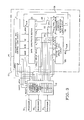
- FIG. 3 illustrates a block diagram of a specific implementation of the System Controller 10 and interface 12 of the transition machine 1 as described in European Patent Application No. r80 102 598.2, Publication No. 19 246.
- the System Controller 10 is seen to comprise a synchronization and control logic circuit 14, a data constructs section 16, a procedure eligibility determination logic circuit 18 and a system status update logic circuit 20.
- Figure 3 also shows the interconnection of each of these major circuit blocks with each other and with the processor/system controller interface 12.
- the processor/system controller interface 12 consists of a number of data and control registers accessible to both the processors 2 and the System Controller 10. The structure and use of these registers are set forth in the following Table 1.
- STATUS - a 4-bit read/write register whose bits are labeled L, I, X and O,and which contains the following synchronization,protocol and mode request information:
- each System Controller there is one set of interface data and control registers as described above. To insure proper operation of each System Controller, no processor may modify these registers while the System Controller is active (i.e., if the L bit in the STATUS re g is- ter is true).
- the processors also must be synchronized so that only one processor modifies these registers at a time. This can be accommodated in various ways, for example, a binary semaphore can be employed to avoid the critical section problem and synchronize the processors.
- a multiport organization can be employed where each processor has a dedicated set of interface registers and a multiport controller resolves multiple processor access contention.
- the multiport controller performs the actual data transfer between the dedicated processor interface registers and the actual system controller registers (similar to the operation of a multiport memory controller). Because of this the processor interface procedures do not require synchronization precautions.
- the multiport controller implementation therefore accommodates a simpler interface description, and is utilized in the following description.
- processors/System Controller interactions There are basically three types of allowed processors/System Controller interactions, namely entry, exit and load transitions. For each type of interaction specific processor actions and System Controller responses are described below.
- a processor When a processor is in an idle state requesting an activity, it will first wait until the logic segment of the System Controller is not busy which is indicated by the L bit in the STATUS register being set false. At that time it will store its processor type identification into the register, TYPEp (if not previously initialized). The X bit in the STATUS register will be set false to indicate a procedure entry is being requested, and the L discrete in the STATUS register will be set true to signal the System Controller to initiate a transition. The processor will then wait until the System Controller has completed its operation which is indicated by the L discrete in the STATUS register being reset false by the System Controller.
- the System Controller When the System Controller detects that a transition is to be initiated (by the L bit in the STATUS register having been set), it will determine whether the entry, exit, or load transition has been specified. If the entry transition is specified, the matrix dot product is performed with the S vector and the R matrix to obtain the next eligible procedure of a type compatible with the processor TYPEp register. If such an eligible procedure is determined its index is stored in the INDEX register, the procedure access pointer is stored in the register EXECUTE, and the data access pointer is stored in the registers READ and WRITE.
- the active protection specification for the procedure (the A vector) is used to update the system status vector to preclude inappropriate simultaneous execution of the same procedure in another processor. If no eligible procedure exists for the processor, the System Controller will set the 0 bit in the STATUS register true. In this case the system status vector remains unchanged. Access authorization to the interface registers is returned to the processor by resetting the L discrete in the STATUS register.
- the processor When the processor detects that access authorization has been given by the L bit of the STATUS register being set false, it first checks to see if any procedures are eligible. This is accomplished by examining the 0 bit in the status register. If the 0 bit is true, indicating no procedures are currently eligible, the processor puts itself into procedure entry mode and reinitiates the entry sequence. If the 0 bit is false, indicating a procedure is eligible, the READ and WRITE registers are obtained to set up the data access linkages, and the EXECUTE register is obtained to set up control linkages. Control is passed to the specified procedure using the EXECUTE register value. The procedure may (in addition to whatever data processing activities are appropriate to it) compute a V register value.
- the processor When a procedure exits, the processor will copy its V register value into the V register of the system controller interface, and set the exit discrete, X, in the STATUS register true to indicate a procedure is being exited. The processor will then activate the System Controller by setting the L discrete in the STATUS register true, and set itself into an entry request mode.
- the System Controller When the System Controller detects that a transition is to be initiated (by the L discrete in the STATUS register having been set) , it will determine whether the entry, exit, or load transition has been specified. If the exit transition is specified, the value in the INDEX register is used to index into the data constructs, providing the data to incorporate the change in the system status vector caused by the exit procedure. The V register is accessed to perform this update. Then the System Controller indicates its readiness to honor further requests by resetting the L discrete in the STATUS register.
- the processor When a load transition is initiated under software control, the processor will first wait until the logic segment of the System Controller is not busy (indicated by the L discrete in STATUS being set false). At that time the processor will store in the INDEX register the number of the row in the System Controller matrices which is to be loaded. The data to be loaded into each of the EXECUTE, READ, WRITE TYPEi, A, T, F, and R matrices will be placed into the corresponding interface registers and the initial S vector will be placed in the V register.
- the load procedure is essentially an application program that transfers the System Controller data constructs from processor main memory to the System Controller.
- the processors sets the I discrete in the STATUS register true to indicate a load transition is being initiated and then activates the System Controller logic by setting the L discrete true in the STATUS register.
- the System Controller 10 is comprised of a synchronization and control logic circuit 14, a data constructs section 16, a procedure eligiblity determination logic circuit 18, and a system status update logic circuit 20. A specific detailed design for each of these four components is described below.
- the data constructs section 16 of the System Controller 10 contains the System Controller memory.
- the memory may comprise eight random access memory modules, one for each of the R, A, F, T, TYPEi, EXECUTE, READ, and WRITE arrays.
- Each element (row) of the R, A, F, and T arrays contains the same number of bits, which is equal to the number of bits which comprise the system status register.
- memory word widths and individual array word-widths can be identical as will become apparent.
- these memories can be either read only (ROM, PROM, etc.) or read/write.
- read/write memories are utilized which are loaded by the processors.
- the procedure eligibility determination logic circuit 18 is contained within the System Controller 10 and contains the combinational logic necessary to determine procedure eligiblity during entry transitions.
- a subsystem is eligible if the type of processor making the request (content of the TYPE interface register) is equivalent to the processor type required by the selected subsystem (content of the TYPEi data bus), and all data conditions in the S vector relevant to enabling the subsystem are true (i.e., the vector resulting from forming the logical "OR" of the ith row of the R array and the current system status vector, S, contains all ones).
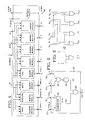
- Figure 5 is a block diagram of the procedure eligibility determination logic.
- line 30 represents a multiple bit data bus which contains the current contents of the TYPEp register in the processor/system controller interface 12.
- Line 32 is a multiple bit data bus which contains the processor type associated with the subsystem currently indexed, namely, TYPEi.
- Line 34 represents a multiple bit data bus which contains the R vector associated with the subsystem currently indexed, namely, Ri.
- Line 36 is a multiple bit data bus from the S register of the data constructs section 16 ( Figure 4) which feeds the current contents of the S register to the procedure eligibility determination logic circuit 18.
- the output of the circuit 18 is a single data bit representative of a single component of the eligibility vector E along output line 38.
- E is logical "1" when the indexed subsystem is eligible and logical "0" otherwise.
- the logical expression for E may be written as follows: Where the symbol ⁇ is used to denote logical equivalence, and j ⁇ 1 denotes the logical "AND" of each element of the vector operated on resulting in a single signal that will be true (i.e., logical "1") if and only if all elements in the vector are true, e.g.,
- the logic circuitry of Figure 5 implements the above equation.
- the signal along data bus lines 30 and 32 are fed to a multibit comparator 40 which produces a single output bit along line 42.
- the output bit is a logical 1 only if the data on the TYPEp data bus (line 30) is idential to the data on the data bus (line 32) corresponding to TYPEi (all bits equivalent), and otherwise the output along line 42 is a logical 0.
- the data bits along bus lines 34 and 36 are input to an OR gate which is represented in Figure 5 by a single conventional OR symbol. It is understood, however, that each of the corresponding bits along lines 34 and 36 are separately OR'ed similar-to the circuit shown in Figure 6.
- the system status update logic-circuit 20 contains the combinational logic required to perform updates to the system status vector, S, appropriate to the transition being initiated. During an entry transition, the logical expression for the S NEW vector generated is:
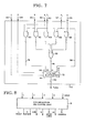
- FIG 7 is a block diagram of the system status update logic circuit 20.
- the system status update logic circuit 20 comprises a plurality of OR and AND logic circuits (See Figure 6 for clarification) identified by numbers 60, 62, 64, 66, 68 and 70.
- AND gates 64, 66, and 68 have one group of inverting input terminals and one group of non-inverting input terminals.
- Element 70 is a multiple input/output OR gate (see Figure 6) wherein each input/output line is a multiple bit data bus.
- the output of OR gate 70 is fed to an input terminal of a 3-to-l multiplexer 72 along lines 74.
- a second group of inputs to multiplex 72 is fed in along lines 76 from the output of AND gate 60.
- a third input is fed to multiplexer 72 along lines 78.
- the output of multiplex 72 is a data bus 80 representative of the new status vector SNEW and is fed to the S register of the data constructs section 16 (see Figures 3 and 4).
- the inputs (generally data buses) to update circuit 20 are fed in along lines 82, 84, 86, 88, 90, 92 and 94.
- Line 82 carries the single bit I discrete value from the system STATUS register of the interface 12.
- Line 84 carries the single X bit from the STATUS register.
- Associated logic circuits include input lines 86, 88, 90, 92 and 94, AND gates 60, 62, 64, 66, 68 and OR gate 70.
- the synchronization and control logic circuit 14 contains the clocked sequential logic required to control the operation and internal connections of all the components of the
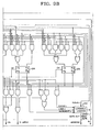
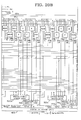
- the various input and output lines associated with the logic circuit 14 are generally shown in Figures 3 and 8 with a detailed schematic diagram illustrated in Figures 9A and 9B.
- the function of the L, I and X bits of the STATUS register and the INDEX register of the interface 12 have been set forth above (see Table I for example).
- ADDRESS, CE, R/W and S LATCH have already been defined (see, for example, Table II). These latter signals are all generated by the synchronization and control logic circuit 14 and fed primarily to the data constructs section 16.
- the ADDRESS bus is also latched into the INDEX register of the interface 12 during entry transitions when an eligible subsystem is detected.
- An ENTRY LATCH signal is a one bit control signal output by the synchronization and control logic circuit 14 to the processor interface registers. This signal causes the current values of the EXECUTE, READ, WRITE and the ADDRESS data buses to be latched into the EXECUTE, READ, WRITE and INDEX register in the processor interface 12. This signal is enabled only during entry transitions when an eligible subsystem is detected.
- the L RESET is a one bit control signal output by the synchronization and control logic circuit 14 to the processor interface registers. When enabled, this signal causes the L discrete of the processor interface STATUS register to be set false (i.e., logical "0").
- the synchronization and control logic circuit 14 enables this signal at the completion of each transition.
- FIG. 9 A specific embodiment of the synchronization and control logic is shown in Figure 9. Other logic combinational arrangements are possible with the design criteria simply being to reproduce the various outputs of Figure 8 with the various possible combinations of the input variables L, I, X, E and INDEX.
- the state diagram is shown in Figure 10. In Figure 10, the symbol ⁇ indicates a "don't care" condition.
- the design of the logic circuit from the state diagram may be done in accordance with well known techniques as set forth, for example, by M. M. Mano, Computer Logic Design, Prentice - Hall, Inc., (1972), pp. 200-236.
- the state assignments utilized in the logic design are as follows:
- the System Controller has three internal modes of operation, one for each of the entry, exit and load transitions.
- the synchronization and control logic circuit 14 begins accessing successive rows (i.e., each successive element of the eight memory modules) of the data construct matrix arrays, causing them to be output on their respective data buses.
- the subsystem eligibility determination logic circuit 18 computes the eligibility of the associated subsystems, and the system status update logic circuit 20 generates the S NEW vector based on the current system status vector and the A vector associated with the subsystem indexed. It will be recalled that the A vector is used to preclude inappropriate simultaneous execution of the same subsystem in another processor.
- the synchronization and control logic circuit 14 causes the S register to latch the S NEW vector, transfers access and control information (i.e., EXECUTEi: READi; WRITER; and ADDRESS) from the associated data buses to the processor interface registers (i.e., into the EXECUTE, READ, WRITE and INDEX registers respectively), and returns access authorization to the processor by resetting the L busy discrete in the interface STATUS register. If no subsystem is found eligible the synchronization and control logic circuit 14 notifies the processor by setting the 0 discrete in the interface STATUS register and returns access authorization to the processor. In this instance, no system status vector update occurs.
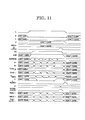
- Figure 11 represents the timing diagram of the control and data signals in the System Controller during an entry transition resulting in an eligible subsystem being detected which is associated with the address row three of the data constructs. It is assumed for the purpose of illustration that each memory array of the data constructs contains only four rows.
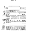
- Figure 12 represents a similar timing diagram for an'entry transition where no subsystem is detected as eligible.
- the synchroniz- tion and control logic circuit 14 accesses one row (i.e., one element from each of the eight memory modules) in the data constructs section 16.
- the value stored in the INDEX register is used as the address to select the appropriate row.
- the system status updated logic circuit 20 generates the S NEW vector from the current S vector, the T, F and A vectors associated with row indexed, and the V vector returned by the processor in the V register of the interface 12.
- the synchornization and control logic circuit 14 causes the S register to latch the S NEW vector and returns access authorization to the processor by resetting the L discrete in the STATUS register.
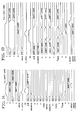
- Figure 13 represents the timing diagram of the control and data signals in the System Controller durng an exit transition.
- the synchronization and control logic circuit 14 first causes .the content of each of the interface data registers, R, A, T, F, EXECUTE, READ, WRITE, V, and TYPEi to be transferred to the associated data buses.
- a row i.e., one element from each of the eight memory modules
- the value stored in the INDEX register of interface 12 is used to select the row accessed. This causes the content of each data bus to be written into the addressed element of the associated memory module.
- the synchronization and control logic circuit 1-4 latches the SNEW vector which is input from the interface 12 V register and returns access authorization to the processor by resetting the L discrete in the STATUS register.
- Figure 14 represents the timing diagram of the control and data signals in the System Controller during a load transition.
- a modular disjoint expansion of the System Controller may be utilized.
- a plurality of System Controllers 10a, 10b, lOc may be utilized each with its associated multiport controller interface 12a, 12b, 12c as shown in Figure 15.
- the configuration is particularly appropriate for batch processing wherein many disjoint computations may be running contemporaneously across all processors. If a processor is locked out of one System Controller, e.g., 10a, it may still be provided access to a subsystem through another System Controller, e. g . 10b.
- Each of the System Controllers 10a, lOb, 10c etc. is configured as shown in Figure 3 and operates to enable subsystems specified within its data construct section independently of the other System Controllers.
- Each data construct section within the System Controllers 10a, lOb, lOc etc. is configured as shown in Figure 4 having its own separate READ, EXECUTE, WRITE, TYPE, A, T, F and R registers independent of the comparable registers in other data construct sections of other System Controllers.
- the complete disjoint configuration of the transition machine of Figure 15 effectively prevents interprocessor access contention. Any convenient number of disjoint System Controllers and corresponding interface registers may be utilized depending upon the size of the processing required.
- the disjoint configuration requires a slight modification to the standard processor/ system controller interface procedure. Specifically, a means of indicating the specific System Controller that contains the data constructs for each active subsystem must be provided. This is required to ensure that when the subsystem exits, the-exit transition is performed by only the System Controller that dispatched the subsystem originally. These are numerous methods to incorporate this capability. For example, with the configuration shown in Figure 15, the processor can maintain an indicator of the specific System Controller which contains the data constructs for the procedure currently being executed. This is facilitated by the fact each set of system controller interface registers are uniquely addressable. The operational flow diagram of the processor interface procedure for this configuration is shown in Figure 15a. This approach requires only a very minor modification to the standard processor/system controller interface logic 12 as shown in Figure 16.
- An additional method of expanding the capability of the System Controller in accordance with the teachings of the invention is to expand the effective size of the data constructs section either horizontally or vertically.
- a horizontal expansion of the data construct capacity enables more data conditions to be utilized, and a vertical expansion of the data construct capacity enables a greater number of subystems to be included within the system, effectively incresing the number of programming steps possible in solving the algorithm.
- modularity is achieved using a plur- laity of fixed word-length conventional memory sections 16, procedure eligibility determination logic circuits 18, system status- update logic circuits 20 and a single synchronization and control logic circuit 14.
- the data constructs section 16 comprises a memory component 1000 in which any one of the various data constructs R, A, T, F, TYPEi, READ, WRITE and EXECUTE can be stored and a separate register component 1002 in which the S vector can be stored.
- the procedure eligiblity determination logic circuit 18 is seen to comprise a type comparison component 1004 and a dot product component 1006.
- the type comparison component compares the two type indicator inputs (TYPEi and TYPEp) for logical equivalence, generating one component of the procedure eligiblity indicator.
- the dot product component 1006 generates another component of the procedure eligibility indicator based on the system status vector (S) and the requirements vector (Ri) which are input thereto.
- a horizontally expandable System Controller 210 and modified interface 212 is illustrated in Figures 19A to 19 C .
- the System Controller 210 is seen to comprise a synchronization and control logic circuit 214, a plurality of data constructs memory components 216a-216t (where at least the memories within each modular unit such as 216e-216h will have compatable characteristics, such as word-width), a plurality of data constructs register components 217a, 217b, 217c, and 217d, a procedure eligibility determination logic type comparison component 219, a plurality of procedure eligibility determination logic dot product components 218a, 218b, 218c, and 218d, and a plurality of status update logic circuits 220a, 220b, 220c and 220d.
- the synchronization and control logic circuit 214 is configured as shown in Figures 9A and 9B; each of the data construct memory components 216 and 217 is configured as shown in Figure 17; each procedure eligibility determination logic circuit component 218 and 219 is configured as shown in Figure 18; and each system status update logic circuit 220 is configured as shown in Figure 7.
- Data construct section components 216e, 2l6f, 216g, 216h, and 217a, procedure eligibility determination logic circuit 218a and the system status update logic circuit 220a form a modular unit 225a as shown by the dotted line in Figure 19A.
- a second modular unit 225b is formed by the data construct section componetns 216i, 216j, 216k, 2161, and 217b, procedure eligibiity determination logic circuit 218b and the system status update logic circuit 220b.
- Additional modular units 225c-and 225d are made up from their elements 216m, 216n, 216 0 , 216p, 217c, 2181c, 220c, and elements 216q, 216r, 216s, 216t, 217d, 218d, and 220d, respectively.
- any number of modular units 225 may be employed as will become clear with respect to the operation of the circuit of Figure 19.
- each of the modular units 225a-225d is identical, the following description is applicable to any one unit, and consequently, no suffix is utilized unless a particular unit is intended.
- the data construct section components 216 and 217, procedure eligibility determination logic circuit component 218 and status update logic circuit 220 are interconnected with one another in a similar fashion as shown in Figure 3.
- the primary difference between the interconnection of the elements between Figure 3 and Figure 19 is the utilization of a multiple input AND gate 227.
- the inputs of AND gate 227 are connected to receive the outputs of the procedure eligibilty determination logic circuit components 218 and 219 along the lines 238a-238e.
- the output of AND gate 227 is fed along a line 239 to the input of a synchronization and control logic circuit 214.
- This input signal to the synchronization and control logic circuit 214 functions the same as the input E signal to synchronization and control logic circuit 14 of Figure 3.
- ANDing all of the outputs of the procedure eligibility determination logic circuit components 218 and 219 of the individual modular units is required inasmuch as each modular unit operates with only a part of the system status vector (a component group of data conditions) , and eligibility of a particular subsystem is only appropriate if each of the partial dot products of the system status vector S and the relevance matrix R indicates a true eligibility. Additionally, the type of processor making the request must be equivalent to the processor type requirement for the indexed subsystem.
- a given subsystem is eligible only if all of the outputs of the procedure eligibility determination logic circuit components 218a-218d and the type comparison component 219 are ANDed together.
- the R, T, F and A matrices as well as the S vector are partitioned by the modular unit arrangement into multiple groups of columns modulo M.
- M is the number of columns available in a modular unit 225, i.e. the number of columns in each of the R, T, F, and A matrices and the S and V vectors within the data construct section components 216 and 217 and is determined by the word-width of the memories that are selected for the particular implementation.
- the interface 212 is configured similar to the interface of Figure 3 but has been expanded to accommodate the modifications as required by the horizontal expansion of the System Controller.
- the interface 212 is seen to comprise a STATUS register 240 and an INDEX register 252 utilized in all entry, exit and load transitions and a READ register 244, WRITE register 246 and EXECUTE register 248 utilized during entry and load transitions. All these registers are used in a similar fashion as described in relation to Figure 3. Additional registers are also utilized such as V registers 250-253 (exit and load transition) and the TYPEp register 255 (entry transition).
- the V register is composed of four separate registers, one for each of the four modular units 225 as illustrated.
- the V vector is effectivley broken down into components modulo M. Components V 0 , V 1 , V 2 , and V 3 are stored respectively in registers 250, 251, 252, and 253. Each component is fed to a separate one of the modular units 225.
- registers of the interface 212 are utilized only during the load transition. These registers comprise the A, T, F, R, and TYPE; registers of Figure 3. For the horizontally expanded System Controller of Figure 19, however, the first four of these registers are likewise broken down modulo M so that again one component of each of these data constructs is fed to each of the modular units 225. For example, the A construct is broken up into components A 0 , A 1' A 2 and A3. Each component is fed to a separate one of the modular units 225. Likewise, the constructs T, F and R are also broken up in a similar fashion. These load registers of the processor/system controller interface must thus be expanded in accordance with the number of modular units 225 utilized in forming the entire System Controller.
- register 260 stores component A 0
- register 261 stores component T 0
- register 262 stores component F O
- register 263 stores component R O .
- a single TYPE i register 264 is connected to the data constructs section memory component 216d that is dedicated for storing the processor type requirements for each subsystem. The TYPE i register 264 is to be distinguished from the entry TYPE register 255.
- a multiplexing arrangement may be utilized where a single interface register would be employed for the run time (entry transition) and load operations. The multiplexing unit would be responsive to the I bit of the status register 240 for example to switch data within the single TYPE register as appropriate for entry or load operations.
- each of these registers may be contiguous as is the V register (contiguous register 250-253 storing components V 0 , V I , V2 and V 3 ).
- the component groups of the modular units 225 generate component procedure eligibility indicators -E 0 , E 1 , E2 and E3 based on the four groups of M data conditions maintained by the entire System Controller.
- the type comparison component 219 also generates a component, designated Et, of the procedure eligibility indicator. For a given subsystem to become eligible for execution it must be found eligible in all component groups. Consequently, each component of. the eligibility indicator E is connected to AND gate 227 and fed to the synchronization and control logic circuit 214 along the line 239.
- the synchronization and control logic circuit 214 operates as in figures 9A and 9B to control the output of the data construct section 216.
- the procedure entry transition continues until an eligible procedure is detected, or it is detected that no procedures are currently eligible. Assuming a subsystem is found eligible, the interface 212 is loaded with the appropriate values of the READ register 216a, WRITE register 216b, and EXECUTE register 216c, the updated S vector is generated and latched in each of the component groups of the modular units 225, and the L busy discrete in the STATUS register 240 is reset.
- V vector returned by any individual processor to the interface 212 may be transferred sequentially into the registers 250-253 by the processor during an exit transition.
- the complete V vector, V 0 , V 1 , V 2 andV3 is then fed in parallel to the modular units 225.
- the data from the load registers namely registers 260-263, 270-273, 280-283 and 290-293 are transferred simultaneously to the appropriate data construct section 216 of the modular units 225.
- the TYPE i register 264 is loaded simultaneously into the TYPE data construct section 216d.
- Data from the registers 244, 246, 248, 250-253 are also transferred simultaneously to the appropriate data constructs sections 216 of the modular units 225.
- the registers 250-253 are used to load the status vector S whose components S 0 , S l , S 2 and S 3 are stored in registers 217a-217d. This loading is achieved via the logic circuit of Figure 7.
- the L bit of the STATUS register 240 is reset.
- the worst case transition time depends only upon the number of rows (N) in the modular unit 225. Effectively, the time required to perform an entry, exit or load transition remains constant and is independent of the horizontal size of the System Controller once the interface registers have been loaded.
- Figures 20-22 illustrate a vertically expanded embodiment of a System Controller 310 and associated interface 312.
- the vertically expanded System Controller comprises a plurality of modular units 325 designated as 325a, 325b, 325c and 325d.
- Each modular unit 325 comprises a plurality of data construct memory components 316, a procedure eligibility determination logic 318 and a system status update logic circuit 320.
- a single synchronization and control logic circuit 314 and a single data constructs register component 317 are employed and are interconnected to the modular units 325 as shown.
- the four circuits 314, 316, 317 and 320 are the same as their counterpart circuits 214, 216, 217 and 220 previously described in relation to Figure 19.
- Circuit 318 is the same as its counterpart circuit 18 shown in Figure 6.
- the matrices A, T, F and R as well as the TYPEp, READ, WRITE and EXECUTE arrays are partitioned into multiple groups of rows modulo N.
- N is the number of rows supported by the standardized component or the modular unit 325.
- Each of these data constructs, modulo N is loaded into a separate data construct memory component 316a1...316a8, 316bl...316b8, 316cl- ...316c8, and 316d1...316d8 through the processor interface registers 312.
- a single system status vector S is maintained in the data. constructs section register component 317 on which each modular unit 325 operates.
- the interface 312 is seen to comprise a STATUS register 340, INDEX register 342, and a plurality of registers identified as READ registers 344, WRITE register 346, EXECUTE register 348, V register 350 and TYPE P register 355.
- the interface 312 also comprises a plurality of registers used only during the load transition. These registers comprise TYPE i registef 360, R register 364, A register 365, T register 366 and F register 367.
- the prime difference between the interface 312 and the previously described interface 212 of Figure 19 or interface 12 of Figure 3 is the utilization of a two-field INDEX register 342.
- the first field of the INDEX register is a group selection field 380
- the second field of the INDEX register 342 is a displacement field 382.
- the group selection' field 380 designates which component group, namely which modular unit 325 contains the row in question (the subsystem being indexed).
- the displacement field 382 designates which row within the selected modular unit 325 actually contains the desired information.
- the group selection field 380 is embodied herein by a two-bit field designation H l and H 2 . Additional logic circuitry is described for selecting the particular modular unit 325 designated by the bits H 1 and H 2 and to multiplex data and control signals appropriately to and from the selected modular unit. In general there will be ⁇ log2N ⁇ bits allocated to the group selection function.. (The nomenclature [ y ] indicates the first integer value greater than or equal to y.)
- the System Controller of Figure 20 further comprises a status selection logic circuit 400, a load control logic circuit 402, an entry/load bidirectional multiplexer 404 and a load multiplexer 406.
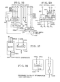
- the status selection logic circuit 400 is shown in detail in Figure 21, and the load control logic circuit 402 is shown in detail in Figure 22.
- the status selection logic circuit 400 is seen to comprise a priority encoder 410, OR gate 412, a two-to-one multiplexer 414, a NOR gate 416 and a status multiplexer 418.
- the priority encoder 410 has input lines 420a-420d connected to receive the outputs E 0 , E l , E 2 , E 3 of the corresponding procedure eligibility determination logic circuits 318a-318d. Liens 420a-420d are also connected to the inputs of the multiple input OR gate 412 which provides a single output E mas ter along a line 422. Line 422 is in turn interconnected as an input to the synchronization and control logic circuit 314 of Figure 20A.
- the output of the priority encoder 410 depends upon the particular values along its input lines 420a-420d.
- the truth table for the priority encoder 410 is shown in the following Table III.
- the binary output of the priority encoder 410 effectively establishes a coded priority sequence such that assuming simultaneous eligibility of subsystems within each modular unit 325, priority is assigned to the first unit, namely modular unit 325a. Absent an eligible subsystem within modular unit 325a the next priority is given to modular unit 325b etc.
- the output of the priority encoder is connected via lines 424a and 424b to multiplexer 414 ( Figure 21) as well as entry/load bidirectional multiplexer 404 ( Figure 20).
- the binary coded output from the priority encoder which feeds the multiplexer 404 effectively routes the address designation values of interest to the READ register 344, WRITE register 346 and EXECUTE register 348 from the approprpiate one of the modular units 325.
- Further inputs to the multiplexer 414 are provided by the multiple input NOR gate 416 along a select line 426.
- the two inputs to the NOR gate 416 are provided by the I and X bits from the STATUS register 340.
- the output of NOR gate 416 is high during an entry transition and low during either an exit or load transition.
- the four data inputs to the multiplexer 414 are provided by the most significant bits of the INDEX register 342, namely, the H l and H 2 bits of the group selection field 380 and the coded output of the priority encoder 410.
- An entry transition provides a high output along the select line 426 effectively passing the signals along the input lines 424a and 424b to the output of the multi- pelxer 414 along lines 428a and 428b.
- the low output signal along the select line 426 effectively feeds the group selection field H 1 , H 2 from the input of the multiplexer 414 to its output along the output lines 428a and 428b.
- lines 428a and 428b are interconnected to the status multiplexer 418.
- Status multiplexer 418 has a plurality of input lines: 430a-430d and a single output line 432.
- the select inputs along lines 428a and 428b determine which of the input lines 430a-430d is fed to the output line 432.
- the truth table for designating operation of the multiplexer 418 is shown below in Table IV.
- the input lines 430a-430d of the multiplexer 418 are fed from the corresponding'outputs of the modular units 325a-325d.
- input lines 430a-430d are fed from the outputs of the system status update logic circuits 320a-320d providing updated system status output signals S 0 , S 1 , S 2 and S 3 respectively.
- the output of the multiplexer 418 is fed as a S new master signal along line 432 ( Figure 20) as an input signal to the data construct register component 317.
- a circuit diagram of the load control logic circuit 402 is shown in Figure 22.
- the load control logic circuit 402 is seen to comprise a binary decoder 440 and a load multiplexer 442.
- the input to the binary decoder 440 is taken from the high order bits of the INDEX register, mainly the group selection field 380. These bits H 1 and H 2 are the same as those utilized in the multiplexer 414 of Figure 21.
- the binary decoder 440 provides output signals along the four lines 44a-444d which are fed to the inputs of the load multiplexer 442.
- the operation of the binary decoder 440 is defined by Table V below.
- the load multiplexer 442 effectively selects between two groups of input lines, each group having four lines therein as determined by the input along a select line 446.
- the operation of the circuits illustrated in Figures 20-24 may be understood in reference to a description of the entry, exit and load transitions.
- all of the component groups namely, the modular units 325 are enabled simultaneously by the common synchronization and control logic circuit 314.
- the modular units 324 generate procedure eligibility indicators E O -E 3 in parallel for the particular row indexed by the synchronization and control logic circuit 314.
- the system status update logic circuits 320a-320d of the modular units 325 generate the updated system status signals Sj-S 3 in parallel for the particular row indexed.
- the synchronization and control logic circuit 314 causes the S new vector for the modular unit 325 containing the eligible subsystem to be latched into the common S register of the data constructs register component 317.
- the selection of which of the vectors SO-S 3 will in fact be passed on as the new system status vector is determined by the priority encoder 410 as per truth Table III.
- multiplexer 414 selects the input lines 424a and 424b (since the output of NOR gate 416 is high) and passes signals generated thereon to its output along lines 428a and 428b. These output lines are, in effect, the select lines for the status multiplexer 418 and are utilized to select one of the status vectors S0 , Sl , S2 and S 3 .
- the synchronization and control logic circuit 314 also addresses each of the data construct memory components 316 for passing the appropriate data to the READ register 344, WRITE register 346 and EXECUTE register 348 of the interface 312.
- Appropriate multiplexing from the data construct sections 316a-316d into the interface READ, WRITE and EXECUTE registers is determined by the entry/load bidirectional multiplexer 404 utilizing again the output of the priority encoder 410.
- a status vector appropriate to that selected modular unit is calculated and the READ, WRITE and EXECUTE addresses are passed from that selected unit to the READ, WRITE and EXECUTE registers of the interface 312.
- the displacement field of the INDEX register 342 is loaded with the row number of the eligible procedure (i.e. ADDRESS) and the group selection field 380 is loaded with the output of the priority encoder 410 (i.e., lines 424a and 424b) which indicates the component group 325 that contains the eligible procedure.
- the 0 bit in the STATUS register 340 is set true, otherwise it is set false.
- the L bit is then set false to allow a subsequent access by processors to the interface 312 and System Controller 310.
- all component groups namely, all of the modular units 325 are enabled simultaneously and generate in parallel an updated system status vector, SO-S 3 , for the row specified by the displacement field 382 of the INDEX register 342.
- the status selection logic circuit 400 selects the appropriate one of the updated status vectors which is to be stored in the data construct register component 317.
- the selection of the status vector for the S new master signal along line 432 is now made by means of the group selection field 380 which provides inputs to the multiplexer 414 ( Figure 17).
- the output of NOR gate 416 is low thereby selecting the H 1 , H 2 bits forming the group selection field 380, and these bits in turn are utilized as the select inputs to the status multiplexer 418 thereby selecting one of the calculated outputs of the system status update logic circuits 320a-320d as the new system status vector.
- the selected calculated output of the system status update logic circuit 320 corresponds to the modular unit 325 being designated by the exiting processor.
- the L bit of the status interface register 340 is then reset to allow subsequent access by the data processors.
- the data from the processor/System Controller interface register 312 is transferred to the particular modular unit 325 specified by the group selection field 380 of the INDEX register 342 and into the particular row of the data construct memory components 316 as specified by the displacement field 382 of the INDEX register 342.
- This selection is performed by the load control logic 402.
- the select line 446 of the load multiplexer 442 is controlled by the I bit of the STATUS register 340.
- I is high (logical 1)
- the lines 444a-444d which feed the load multiplexer 442 are passed to the output lines 448a-448d.
- the code present on the input lines 444a-444d is generated by the binary decoder 440 in response to the code of the group selection field 380 as per Table V.
- the output of the load multiplexer 442 along the output lines 448a-448d control the CE terminals of the data construct section 416a-416d, respectively.
- the load control logic circuit 402 controls which of the data construct sections 416 will be enabled for loading data along its input lines.
- the data loaded into the data construct memory components 316 is fed by means of the registers of the interface 312. These registers include the TYPEi register 360, READ register 344, WRITE register 346, EXECUTE register 348, R register 364, A register 365, T register 366 and F register 367.
- the inputs from these registers are multiplexed into the modular units 325 by means of the load multiplexer 406 and the entry/load bidirectional multiplexer 404.
- the load multiplexer has its select lines controlled by the group selection field 380 of the INDEX register 342. This establishes a data path from the interface registers 360, 364, 365, 366 and 367 to only the data constructs memory components 316a-316d that are to be loaded.
- the select lines of the entry/load multiplexer 404 are also set equal to the group selection field 380 ' of the INDEX register during load transitions, as described previously in relation to the status selection logic of Figure 21.
- a data path is therefore, also established from the interface registers 344, 346 and 348 by the entry/load bidirectional multiplexer 404 to only the data constructs memory components 316a-316d that are to be loaded.
- only the appropriate data construct sections 316a-316d is enabled and loaded by the load registers of the interface 312.
- the L bit of the status interface register 340 is reset, completing the load transition. It is to be noted that during the load transition, the status selection logic circuit 400 permits the current value of the V interface register to be fed as an output S new master along line 432 therefore providing an input to the data construct section register component 317 for loading the initial system status vector.
- the worst case transition time depends only upon the number of rows N in the modular unit 325.
- the time required to perform an entry or exit transition remains constant independent of the total number of rows maintained by the System Controller.
Landscapes
- Engineering & Computer Science (AREA)
- Software Systems (AREA)
- Theoretical Computer Science (AREA)
- Physics & Mathematics (AREA)
- General Engineering & Computer Science (AREA)
- General Physics & Mathematics (AREA)
- Multi Processors (AREA)
- Bus Control (AREA)
Applications Claiming Priority (2)
| Application Number | Priority Date | Filing Date | Title |
|---|---|---|---|
| US128878 | 1980-03-10 | ||
| US06/128,878 US4379326A (en) | 1980-03-10 | 1980-03-10 | Modular system controller for a transition machine |
Publications (2)
| Publication Number | Publication Date |
|---|---|
| EP0035778A2 true EP0035778A2 (de) | 1981-09-16 |
| EP0035778A3 EP0035778A3 (de) | 1982-09-01 |
Family
ID=22437423
Family Applications (1)
| Application Number | Title | Priority Date | Filing Date |
|---|---|---|---|
| EP81101657A Withdrawn EP0035778A3 (de) | 1980-03-10 | 1981-03-06 | Modulares Steuersystem für eine Übergangsmaschine |
Country Status (5)
| Country | Link |
|---|---|
| US (1) | US4379326A (de) |
| EP (1) | EP0035778A3 (de) |
| JP (1) | JPS57500396A (de) |
| CA (1) | CA1156766A (de) |
| WO (1) | WO1981002645A1 (de) |
Cited By (2)
| Publication number | Priority date | Publication date | Assignee | Title |
|---|---|---|---|---|
| EP0251584A3 (de) * | 1986-06-26 | 1990-04-25 | Nortel Networks Corporation | Synchronisationsverwaltung für ein verteiltes Betriebssystem oder ähnliche Systeme |
| WO1992004677A1 (en) * | 1990-09-12 | 1992-03-19 | Cray Research, Inc. | Fault tolerant networking architecture |
Families Citing this family (12)
| Publication number | Priority date | Publication date | Assignee | Title |
|---|---|---|---|---|
| US4814979A (en) * | 1981-04-01 | 1989-03-21 | Teradata Corporation | Network to transmit prioritized subtask pockets to dedicated processors |
| US4777590A (en) * | 1984-10-29 | 1988-10-11 | Pictorial, Inc. | Portable computer |
| US5021947A (en) * | 1986-03-31 | 1991-06-04 | Hughes Aircraft Company | Data-flow multiprocessor architecture with three dimensional multistage interconnection network for efficient signal and data processing |
| US5201057A (en) * | 1987-01-22 | 1993-04-06 | Uht Augustus K | System for extracting low level concurrency from serial instruction streams |
| US5010482A (en) * | 1987-07-02 | 1991-04-23 | Unisys Corp. | Multi-event mechanism for queuing happened events for a large data processing system |
| US4964042A (en) * | 1988-08-12 | 1990-10-16 | Harris Corporation | Static dataflow computer with a plurality of control structures simultaneously and continuously monitoring first and second communication channels |
| DE69024753T2 (de) * | 1989-10-31 | 1996-05-30 | Hewlett Packard Co | Tragbarer, Ressourcen teilender Datei-Server, der gemeinsame Routines benutzt |
| US5664192A (en) * | 1994-12-14 | 1997-09-02 | Motorola, Inc. | Method and system for accumulating values in a computing device |
| US6253228B1 (en) * | 1997-03-31 | 2001-06-26 | Apple Computer, Inc. | Method and apparatus for updating and synchronizing information between a client and a server |
| US6378029B1 (en) | 1999-04-21 | 2002-04-23 | Hewlett-Packard Company | Scalable system control unit for distributed shared memory multi-processor systems |
| US6597692B1 (en) | 1999-04-21 | 2003-07-22 | Hewlett-Packard Development, L.P. | Scalable, re-configurable crossbar switch architecture for multi-processor system interconnection networks |
| US6263415B1 (en) | 1999-04-21 | 2001-07-17 | Hewlett-Packard Co | Backup redundant routing system crossbar switch architecture for multi-processor system interconnection networks |
Family Cites Families (12)
| Publication number | Priority date | Publication date | Assignee | Title |
|---|---|---|---|---|
| USRE26171E (en) | 1962-03-02 | 1967-03-07 | Multiprocessing computer system | |
| US3343135A (en) * | 1964-08-13 | 1967-09-19 | Ibm | Compiling circuitry for a highly-parallel computing system |
| US3480914A (en) * | 1967-01-03 | 1969-11-25 | Ibm | Control mechanism for a multi-processor computing system |
| US3496551A (en) * | 1967-07-13 | 1970-02-17 | Ibm | Task selection in a multi-processor computing system |
| US3593300A (en) * | 1967-11-13 | 1971-07-13 | Ibm | Arrangement for automatically selecting units for task executions in data processing systems |
| US3560934A (en) * | 1969-06-10 | 1971-02-02 | Ibm | Arrangement for effecting vector mode operation in multiprocessing systems |
| US3643227A (en) * | 1969-09-15 | 1972-02-15 | Fairchild Camera Instr Co | Job flow and multiprocessor operation control system |
| US3648252A (en) * | 1969-11-03 | 1972-03-07 | Honeywell Inc | Multiprogrammable, multiprocessor computer system |
| US3648253A (en) * | 1969-12-10 | 1972-03-07 | Ibm | Program scheduler for processing systems |
| US4073005A (en) * | 1974-01-21 | 1978-02-07 | Control Data Corporation | Multi-processor computer system |
| US4189771A (en) * | 1977-10-11 | 1980-02-19 | International Business Machines Corporation | Method and means for the detection of deadlock among waiting tasks in a multiprocessing, multiprogramming CPU environment |
| US4319321A (en) * | 1979-05-11 | 1982-03-09 | The Boeing Company | Transition machine--a general purpose computer |
-
1980
- 1980-03-10 US US06/128,878 patent/US4379326A/en not_active Expired - Lifetime
-
1981
- 1981-03-06 EP EP81101657A patent/EP0035778A3/de not_active Withdrawn
- 1981-03-09 CA CA000372549A patent/CA1156766A/en not_active Expired
- 1981-03-10 JP JP56501188A patent/JPS57500396A/ja active Pending
- 1981-03-10 WO PCT/US1981/000297 patent/WO1981002645A1/en not_active Ceased
Cited By (3)
| Publication number | Priority date | Publication date | Assignee | Title |
|---|---|---|---|---|
| EP0251584A3 (de) * | 1986-06-26 | 1990-04-25 | Nortel Networks Corporation | Synchronisationsverwaltung für ein verteiltes Betriebssystem oder ähnliche Systeme |
| WO1992004677A1 (en) * | 1990-09-12 | 1992-03-19 | Cray Research, Inc. | Fault tolerant networking architecture |
| US5206952A (en) * | 1990-09-12 | 1993-04-27 | Cray Research, Inc. | Fault tolerant networking architecture |
Also Published As
| Publication number | Publication date |
|---|---|
| WO1981002645A1 (en) | 1981-09-17 |
| JPS57500396A (de) | 1982-03-04 |
| CA1156766A (en) | 1983-11-08 |
| EP0035778A3 (de) | 1982-09-01 |
| US4379326A (en) | 1983-04-05 |
Similar Documents
| Publication | Publication Date | Title |
|---|---|---|
| EP0035778A2 (de) | Modulares Steuersystem für eine Übergangsmaschine | |
| US5129077A (en) | System for partitioning a massively parallel computer | |
| Gottlieb et al. | Basic techniques for the efficient coordination of very large numbers of cooperating sequential processors | |
| US5535408A (en) | Processor chip for parallel processing system | |
| KR960016880B1 (ko) | 연관 병렬 처리 시스템 | |
| US4695943A (en) | Multiprocessor shared pipeline cache memory with split cycle and concurrent utilization | |
| US5142676A (en) | Separate content addressable memories for storing locked segment addresses and locking processor identifications for controlling access to shared memory | |
| US4709327A (en) | Parallel processor/memory circuit | |
| US5123109A (en) | Parallel processor including a processor array with plural data transfer arrangements including (1) a global router and (2) a proximate-neighbor transfer system | |
| US4598400A (en) | Method and apparatus for routing message packets | |
| US5586331A (en) | Duplicated logic and interconnection system for arbitration among multiple information processors | |
| US5212773A (en) | Wormhole communications arrangement for massively parallel processor | |
| EP0214718A2 (de) | Digitalrechner | |
| EP0132926A2 (de) | Parallel-Prozessor | |
| US6334177B1 (en) | Method and system for supporting software partitions and dynamic reconfiguration within a non-uniform memory access system | |
| EP0213694A2 (de) | Digitalrechner mit Cache-Speicher, welcher zur gleichzeitigen Mehrzugriffsverarbeitung aus parallelen Prozessoren geeignet ist | |
| US3943494A (en) | Distributed execution processor | |
| US4319321A (en) | Transition machine--a general purpose computer | |
| RU2042193C1 (ru) | Вычислительная система | |
| US4949243A (en) | Data processing system intended for the execution of programs in the form of search trees, so-called or parallel execution | |
| EP0363882B1 (de) | Multiprozessorsystem mit Verwendung von einem Kommunikationsregister mit den Prozessoren zugeordneten Speicherstellen | |
| US5465369A (en) | Network structure for parallel software processing | |
| EP0880740B1 (de) | Integrierte schaltung für multitaskingsunterstützung in einfach- oder mehrfachprozessornetzwerken | |
| Schanin | The design and development of a very high speed system bus—the encore Mutlimax nanobus | |
| EP0394362A4 (en) | Method and apparatus for aligning the operation of a plurality of processors |
Legal Events
| Date | Code | Title | Description |
|---|---|---|---|
| PUAI | Public reference made under article 153(3) epc to a published international application that has entered the european phase |
Free format text: ORIGINAL CODE: 0009012 |
|
| AK | Designated contracting states |
Designated state(s): AT BE CH DE FR GB IT LI LU NL SE |
|
| PUAL | Search report despatched |
Free format text: ORIGINAL CODE: 0009013 |
|
| AK | Designated contracting states |
Designated state(s): AT BE CH DE FR GB IT LI LU NL SE |
|
| 17P | Request for examination filed |
Effective date: 19830131 |
|
| STAA | Information on the status of an ep patent application or granted ep patent |
Free format text: STATUS: THE APPLICATION IS DEEMED TO BE WITHDRAWN |
|
| 18D | Application deemed to be withdrawn |
Effective date: 19850726 |
|
| RIN1 | Information on inventor provided before grant (corrected) |
Inventor name: ANASTAS, MARK STEVEN Inventor name: VAUGHAN, RUSSELL FREDRICK |