EP0036933A2 - Connecteur enfichable et son application à l'établissement d'une connexion électrique déconnectable - Google Patents
Connecteur enfichable et son application à l'établissement d'une connexion électrique déconnectable Download PDFInfo
- Publication number
- EP0036933A2 EP0036933A2 EP81100942A EP81100942A EP0036933A2 EP 0036933 A2 EP0036933 A2 EP 0036933A2 EP 81100942 A EP81100942 A EP 81100942A EP 81100942 A EP81100942 A EP 81100942A EP 0036933 A2 EP0036933 A2 EP 0036933A2
- Authority
- EP
- European Patent Office
- Prior art keywords
- elements
- contact elements
- contact
- elastic
- circuit board
- Prior art date
- Legal status (The legal status is an assumption and is not a legal conclusion. Google has not performed a legal analysis and makes no representation as to the accuracy of the status listed.)
- Withdrawn
Links
Images

Classifications
-
- H—ELECTRICITY
- H01—ELECTRIC ELEMENTS
- H01R—ELECTRICALLY-CONDUCTIVE CONNECTIONS; STRUCTURAL ASSOCIATIONS OF A PLURALITY OF MUTUALLY-INSULATED ELECTRICAL CONNECTING ELEMENTS; COUPLING DEVICES; CURRENT COLLECTORS
- H01R12/00—Structural associations of a plurality of mutually-insulated electrical connecting elements, specially adapted for printed circuits, e.g. printed circuit boards [PCB], flat or ribbon cables, or like generally planar structures, e.g. terminal strips, terminal blocks; Coupling devices specially adapted for printed circuits, flat or ribbon cables, or like generally planar structures; Terminals specially adapted for contact with, or insertion into, printed circuits, flat or ribbon cables, or like generally planar structures
- H01R12/70—Coupling devices
- H01R12/82—Coupling devices connected with low or zero insertion force
- H01R12/85—Coupling devices connected with low or zero insertion force contact pressure producing means, contacts activated after insertion of printed circuits or like structures
-
- H—ELECTRICITY
- H01—ELECTRIC ELEMENTS
- H01R—ELECTRICALLY-CONDUCTIVE CONNECTIONS; STRUCTURAL ASSOCIATIONS OF A PLURALITY OF MUTUALLY-INSULATED ELECTRICAL CONNECTING ELEMENTS; COUPLING DEVICES; CURRENT COLLECTORS
- H01R12/00—Structural associations of a plurality of mutually-insulated electrical connecting elements, specially adapted for printed circuits, e.g. printed circuit boards [PCB], flat or ribbon cables, or like generally planar structures, e.g. terminal strips, terminal blocks; Coupling devices specially adapted for printed circuits, flat or ribbon cables, or like generally planar structures; Terminals specially adapted for contact with, or insertion into, printed circuits, flat or ribbon cables, or like generally planar structures
- H01R12/70—Coupling devices
- H01R12/71—Coupling devices for rigid printing circuits or like structures
- H01R12/72—Coupling devices for rigid printing circuits or like structures coupling with the edge of the rigid printed circuits or like structures
- H01R12/721—Coupling devices for rigid printing circuits or like structures coupling with the edge of the rigid printed circuits or like structures cooperating directly with the edge of the rigid printed circuits
-
- Y—GENERAL TAGGING OF NEW TECHNOLOGICAL DEVELOPMENTS; GENERAL TAGGING OF CROSS-SECTIONAL TECHNOLOGIES SPANNING OVER SEVERAL SECTIONS OF THE IPC; TECHNICAL SUBJECTS COVERED BY FORMER USPC CROSS-REFERENCE ART COLLECTIONS [XRACs] AND DIGESTS
- Y10—TECHNICAL SUBJECTS COVERED BY FORMER USPC
- Y10T—TECHNICAL SUBJECTS COVERED BY FORMER US CLASSIFICATION
- Y10T29/00—Metal working
- Y10T29/49—Method of mechanical manufacture
- Y10T29/49002—Electrical device making
- Y10T29/49117—Conductor or circuit manufacturing
- Y10T29/49169—Assembling electrical component directly to terminal or elongated conductor
Definitions
- the invention relates to a connector for producing a releasable electrical connection between a plurality of mutually electrically insulated first contact elements and an equal number of second contact elements according to the preamble of claim 1 and the use of the connector.
- Metal springs for example made of spring bronze, serve as contact elements of the female connectors. At the same time, they fulfill the three functions of power conduction, contacting and generating the contact pressure necessary for contacting.
- the contact pressure required for perfect contacting is relatively large. In the case of longer plug strips, a total force for spreading the springs must therefore be applied when plugging in a circuit board, which is quite considerable. This force must be overcome when the circuit board is inserted by pressing the springs apart with the beveled circuit board edges.
- the circuit board material for example glass fiber reinforced epoxy resin
- the sharp edges of the conductor tracks due to the etching processes the contact surfaces of the springs wear out noticeably.
- the dimensions of the springs must be kept relatively large so that sufficient spring forces can be permanently guaranteed. This in turn prevents a reduction in the size of the connector strips or an increase in the contacts with the same size.
- zero force connectors for example from Cannon, DL series
- the contact pressure between the contact elements of the one and the other plug-in element required for contacting is generated externally by a force transmitter, for example by an eccentric, after the force-free insertion.
- the zero-force connectors are subject to minimal wear and tear and ensure a uniform contact force for all contact elements.
- the zero-force plug connectors must be accessible from two places, on the one hand for inserting the plate to be contacted and on the other hand for operating the force transmitter.
- Another disadvantage is that the contact surfaces do not or only slightly rub against each other during the production of the contact and the self-cleaning effect caused thereby is small.
- a connector is known from European patent application 0014511 (application no. 80 200 104.0), in which the contact elements only have the properties of current conduction and contacting, while the contact pressure required for contacting is applied by means of a force deflector during the insertion process.
- This force deflector is a permanently elastic element that is pressed together over profile surfaces when the circuit board to be contacted is inserted. Because of the profile surface shape, the force deflector deviates transversely to the plug-in direction and presses the one or other contact elements that are meanwhile adjacent to one another. A snap connection holds the arrangement in the pushed-together state against the restoring force of the permanently elastic element.
- the object of the invention is therefore to specify a plug connector "in which the plate to be contacted can be inserted via a plug-in opening as in a conventional female connector, but the contact elements do not exert any direct force against one another.
- the contact forces should instead be used during and by the The connector that fulfills this task is characterized by the characterizing part of the first claim.
- Claims 2 to 12 represent special embodiments.
- Claim 13 finally makes statements about the use of the connector.
- the connector thus has properties that combine the advantages of today's female connectors with the advantages of zero-force connectors. This means establishing the plug connection with a single handle, careful handling of the contact surfaces at the start of the plugging process, reduced and not suddenly changing plugging forces, sufficient grinding to ensure safe contact towards the end of the plugging process and secure mounting of the inserted plate without a complicated holding mechanism.
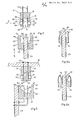
- FIG. 1 shows a perspective view of a plug connector, which is composed of a socket strip 11 and an associated, directly pluggable circuit board 23 to be contacted with the socket strip 11.
- the socket strip 11 forms a (first) carrier element for first contact elements and the printed circuit board 23 a (second) carrier element for second contact elements.
- connection pins 15 denotes a plurality of connecting pins arranged in two rows next to one another, of which only the four delimiting pins are drawn. These connection pins can be designed to connect plugged, soldered, crimped or other connections.
- Each connector pin 15 is connected to a (first) contact element in the interior of the base body 12 or forms a unit with the latter. The desired electrical connection between the connecting pins 15 and the printed conductor lines 29 of the printed circuit board 23 is established via these (first) contact elements.
- the circuit board 23 to be contacted can be inserted into the base body 12 from below via a plug-in opening 17 hidden in FIG. 1, corresponding to the position of the socket strip 11, the circuit board being guided through the plug-in opening.
- Each of the two longitudinal walls of the base body 12 has a slot opening 19 running parallel to the longitudinal edge, through which one or more elastic elements 31 protrude beyond the flat longitudinal sides 20 of the base body, which are oriented parallel to the plugging direction.
- the printed circuit board 23 carries on both sides conductor tracks 29 which, as in known, directly pluggable boards, each end in a row of parallel contact strips 30 on a projection 22 of the board 23. These contact strips 30 form the (second) contact elements of the printed circuit board. They are covered on both sides of the plate by a clamp element 37. These clamp elements are rigidly connected to the printed circuit board 23 via rivets or screws 36. During the insertion process, they slide over the elastic elements 3 1 , which - as described - protrude beyond the flat longitudinal sides 20 of the base body 12. Here, these elastic elements are pressed inwards and deformed elastically.
- Fig. 2 shows the socket strip 11 and the circuit board 23 in section transverse to their longitudinal directions.
- the designations correspond to those of Fig. L.
- the base body 12 of the socket strip 11 is hollow.
- the cavity 21 there are the already mentioned (first) contact elements 25 as an extension of the connection pins 15 in two rows. These can be individual contact lugs or combined conductors in the form of flexible, printed circuit boards, the contact surfaces facing each other and inwards.
- the contact elements 25 are weakly elastic. The elasticity serves to hold the contact elements in the rest position in the direction of the double arrow C, so that the cavity 21 is open in the width of the plug opening 17.
- the corner edges 28 of the base body 12 also help here. However, the elasticity does not serve to generate a pressing force when the printed circuit board 23 is inserted.
- 31 are elastic elements, for example elastic profile elements made of silicone rubber. They are captively stored in the suitably shaped slot openings 19 in the flat longitudinal walls of the base body 12 so that their areas 33 protrude clearly from the openings 19 over the long sides 20 and on the other hand lightly touch the (first) contact elements 25 inside the socket strip 11 .
- the circuit board 23 is designed as a conventional, two-sided, printed circuit board.
- the protrusion 22 carries - as described - the (second) contact elements 30. These are printed, parallel juxtaposed conductor lines which end at the protrusion 22. 37 are the mirror symmetry on the two sides of the circuit board 23 rigidly fastened clamp elements which have an L-shaped cross section.
- Each clamp element 37 forms, together with the associated (second) contact elements 30 and the projection 22, a U-shaped clamp.
- One leg of the clip is formed by the free area 39 of the clip element 37, the other, approximately the same length by the projection 22 with the contact strips 30 and the arc of the U through the attachment area 38 of the clip element 37.
- the open end of the clip points in the direction of insertion, which is indicated by an arrow S.
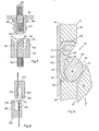
- Fig. 3 illustrates this on a larger scale.
- a (first) contact element 25 and an elastic element 31 touching it are shown, the total thickness of which is transverse to the insertion direction S has the "active thickness" D.
- D is significantly greater than the sum W of the wall thickness of the base body 12 plus the thickness of the contact element 25 or the distance of the plug opening from the outer wall.
- the clear width I transverse to the direction of insertion S between the wedge tip 41 and the (second) contact elements 30 is significantly larger than D.
- the clear width continuously decreases, becoming D at point P.
- the wedge tips 41 contactlessly touch the elastic elements 31, only touch them when the contact strips 30 lie next to the (first) contact elements 25, increasingly deform the elastic elements as the plugging process progresses, and push them across to the plugging direction S into the interior of the socket strip 11.
- the pressure on the elastic elements 31 increases, as a result of which they exert increasing pressure against the (first) contact elements 25.
- these are pressed against the contact strips 30, which rigidly absorb the pressure together with the projection 22.
- the elastic elements 31 are maximally deformed by the regions of constant internal width 43 and pressed into the interior of the socket strip 11.
- the force with which the contact surfaces of the first 25 and second 30 contact elements are pressed against one another depends on the dimensions D, I and II and the properties of the elastic elements 31.
- FIG. 4 shows some examples of cross-sectional shapes of the elastic elements 31, which are essentially in the form of strands.
- the cross section is circular, after b tubular, after c trapezoidal, after d triangular with rounded corners, after e circular, with notches at regular intervals from one side and after f such that the shape cannot be described in one word is.
- These strand-shaped profile materials are inserted into the slot openings 19 of the socket strip 11 in such a way that - as described - they protrude laterally from the flat longitudinal wall.
- the shape of the profile material is selected so that the elastic elements are held captively and essentially immovably in the slot openings 19. If an elastic element according to FIG. 4e is used, the slot openings 19 can be divided into a lattice shape, which increases the stability of the socket strip 11.
- the invention is not exhausted by this socket strip 11 and the circuit board 23 cooperating therewith. Rather, there is a significant number of other connectors that also meet the requirements mentioned.
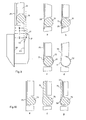
- FIG. 5 shows a socket and a connector strip for an indirectly pluggable printed circuit board.
- 12 is in turn the basic body of the socket strip 11, the connection pins 15 of which are mechanically and electrically connected, for example, to a supporting connecting plate 16 by soldering.
- In the interior of the base body 12 there are two rows (first) contact elements 25, the contact surfaces of which point inwards, as an extension of the connecting pins 15. Slit openings 19 are again contained in the side walls, in which strand-shaped elastic elements 31 are arranged.
- the socket strip of FIG. 2 the socket strip of FIG.
- FIG. 5 shows, as a counterpart to the socket strip 11, a printed circuit board 23 to which a knife strip 47 is fastened on the side.
- This carries two rows of individual pins 48 lying side by side, the contact surfaces of which point outwards and the ones located outside the bar. Terminal ends are bent at right angles and soldered to the circuit board 23.
- the individual pins 48 are on the side of one Surround U-shaped bracket element, which forms the base body of the male connector 47. Both legs 40 of the U are chamfered on the inside and each have a wedge tip 41, a wedge area 42 and then an area adjacent to this. constant clear width 43.
- each leg 40 forms a U-shaped bracket with the associated individual pins 48.
- the clear widths 1 and II transverse to the direction of insertion are larger or smaller than the active thickness D from the sum of the thicknesses of the first contact elements 25 and the elastic elements 31 of the socket strip 11.
- the rigid counterpressure is applied by the center piece 45, on which the individual pins 48 slide along when inserted and to which they are pressed by the deformation force of the elastic elements 31.
- the middle piece 45 can be transferred from the socket strip 11 into the male connector 47, where it is arranged between the two rows of pins 48 so that it touches the pins.
- the plug-in openings 46 of the socket strip 11 combine to form a single opening, the side walls of this opening being able to have small grooves and webs, which in turn provide exact guidance of the second contact elements, i.e. of the pins 48 accomplish.
- the rigid counterpressure is applied by the middle piece combined with the pins 48.
- FIGS. 1, 2 ; 3 and 5 show variants for bracket elements,. where the properties "clamp” is combined with the additional property “exert elastic pressure”.
- the clamp elements consist of springs 53 and 54, which replace the rigid U-legs of FIGS. 1, 2 ; 3 and 5 kick.
- the other U-leg is - as described with reference to FIG. 2 - formed by the projection 22 of the circuit board 23 and the contact strips 30 located thereon.
- the U-legs, ie the springs 53 and 54 and the printed circuit board 23, are connected by rigid block pieces 55.
- the shape of the inside of the springs 53 and 54 is designed in such a way that at the open end of each U-shaped bracket there is a clear width transversely to the direction of insertion, which is greater than the active thickness D, which is defined on the basis of FIG. 3, while the more inner area has a clear width that is smaller than D.
- This pushes the open end of the U-shaped clamps does not come into contact with the elastic elements of the assigned socket strip 11 during the plugging process of the springs 53 and 54. Since these springs can be constructed with a relatively long stroke, the requirements for the mechanical tolerances can be reduced in this way.
- the round socket 80 can be fastened to a support, for example a sheet metal, by means of a flange 81.
- 82 are connection pins which end in the interior of the round socket in weakly elastic contact tabs 83, the contact surfaces of which point inwards.
- the contact lugs 83 are surrounded on the outside by a tubular, rubber-elastic elastic element 85, which is thickened like a bead at the height of the contact surfaces and which is ring-shaped and clamped at the height of the flange by the collar 86 of the flange 81.
- the circular connector 90 can be plugged together with the circular socket 80. It consists of a central, cylindrical middle part 91, which is surrounded on its circumference by second contact elements 92 running parallel to the axis. The Contact surfaces of these second contact elements 92 point outwards and the extension of the contact elements form connecting pins 94.
- the central part 91 is surrounded concentrically by a clamp element 95, which is chamfered inwards at its free end in a wedge shape. This results in a circular wedge tip -96 and a corresponding wedge area 97, to which an area 98 of constant diameter adjoins on the inside.
- the round plug 90 beaks with its middle part 91 and its wedge tip 96 without force at the start of the plugging process.
- the wedge region 97 deforms the bead of the tubular elastic element 85 and presses it inwards.
- the contact tabs 83 are pressed against the second contact elements 92.
- the region of constant diameter 98 deforms the elastic element 85 to a maximum, in such a way that no force component occurs on the circular connector 90 against the direction of insertion.
- FIG. 8 shows, as a further example of a plug connector, two identical socket strips 100 which can be plugged together.
- These carry contact elements 101 which, when pushed into one another, touch with their contact surfaces.
- the elastic elements 102 and the clamp elements 103 mutually absorb the respective counter pressure in such a way that no force component results; which could cause the two socket strips 100 to be pushed apart.
- the pushing together of the two socket strips 100 is made possible by the wedge-shaped design of the clamp elements 103, which have wedge regions 104 at their free end, which enable the two socket strips to be snapped on without force.
- Fig. 9 is a section - enlarged compared to the other figures - a section of the longitudinal wall of a female connector 11 with the slot opening 19 is shown.
- an elastic element 60 is clamped in concave recesses 58 and 59 of the side wall under slight prestress.
- the elastic element has a cross section which has the shape of an approximate oval, with which oval part 61 a comet-like linear part 62, which widens outward in a wedge shape, is homogeneously connected.
- the elastic element 60 braces with the end of the linear part 62 in the concave recess 58 and with the connecting region 70 'between the linear part 62 and the oval part 61 at the recess 59.
- the linear part 62 also closes in this way from its approximately flat outside 63 the slot opening 19 to the inside 64 of the socket strip 11 and touches the contact element 25 on the back.
- the oval part 61 protrudes with its pressure region 65 clearly beyond the outer wall 66 of the socket strip 11. Between the inside 67 of the oval part 61 and the inside 68 of the linear part 62 there is a wedge-shaped slot 69 which is open to the outside.
- the rolling movement of the oval part can be additionally secured or slipping can be avoided by designing the inner sides 67 and 68 to be toothed, so that a toothed, play-free connection is produced during the rolling movement. Accordingly, a possible sliding movement between the pressure region 65 of the oval part 61 and the clamp element 37 can be prevented by making the surface of the clamp element 37, ie the wedge region 42 and the region 43 of constant internal width slightly toothed or roughened, also matched to a corresponding one Design of the surface of the oval part 61.
- the oval part 61 rolls in the opposite direction and in turn lies against the concave recess 59 at the lower end of the slot opening 19 with slight pretension.
- the elastic element 60 can be designed such that when the oval part 61 rolls on the inside 68 of the linear part 62, the sum of the active diameter of the oval part 61 and the active width of the linear part 62 remains constant. In this case, the deformation necessary for the application of the contact force takes place by reducing the clear width of the clamp element 37. With less variation of the clear width of the clamp element 37, the production of an elastic deformation of the elastic element 60 is also possible in that by suitable shaping of the Oval part 61 and / or the linear part 62 increases the active total diameter of both parts during the rolling process.
Landscapes
- Coupling Device And Connection With Printed Circuit (AREA)
Applications Claiming Priority (2)
| Application Number | Priority Date | Filing Date | Title |
|---|---|---|---|
| CH2461/80 | 1980-03-28 | ||
| CH246180 | 1980-03-28 |
Publications (2)
| Publication Number | Publication Date |
|---|---|
| EP0036933A2 true EP0036933A2 (fr) | 1981-10-07 |
| EP0036933A3 EP0036933A3 (fr) | 1981-12-02 |
Family
ID=4234342
Family Applications (1)
| Application Number | Title | Priority Date | Filing Date |
|---|---|---|---|
| EP81100942A Withdrawn EP0036933A3 (fr) | 1980-03-28 | 1981-02-11 | Connecteur enfichable et son application à l'établissement d'une connexion électrique déconnectable |
Country Status (2)
| Country | Link |
|---|---|
| US (1) | US4373764A (fr) |
| EP (1) | EP0036933A3 (fr) |
Cited By (5)
| Publication number | Priority date | Publication date | Assignee | Title |
|---|---|---|---|---|
| FR2662862A1 (fr) * | 1990-05-29 | 1991-12-06 | Kel Kk | Connecteur, notamment pour circuits en forme de pellicules. |
| EP0999613A1 (fr) * | 1998-11-06 | 2000-05-10 | Framatome Connectors International | Prise de connexion sur circuit imprime, comprenant une fiche et une embase |
| US6919111B2 (en) | 1997-02-26 | 2005-07-19 | Fort James Corporation | Coated paperboards and paperboard containers having improved tactile and bulk insulation properties |
| EP2634864A3 (fr) * | 2012-03-02 | 2014-05-21 | Robert Bosch GmbH | Dispositif à plaquettes et agencement électrique correspondant |
| CN113875093A (zh) * | 2019-03-25 | 2021-12-31 | 哈廷电子有限公司及两合公司 | 插接连接器 |
Families Citing this family (27)
| Publication number | Priority date | Publication date | Assignee | Title |
|---|---|---|---|---|
| US4653823A (en) * | 1985-09-13 | 1987-03-31 | At&T Information Systems, Inc. | Electrical connector apparatus |
| CA1306025C (fr) * | 1988-02-15 | 1992-08-04 | Itt Industries Limited | Connecteurs pour conducteurs isoles |
| TW238431B (fr) * | 1992-12-01 | 1995-01-11 | Stanford W Crane Jr | |
| US5435735A (en) * | 1993-02-22 | 1995-07-25 | The Whitaker Corporation | Catalytic converter sensor connector |
| US5391089A (en) * | 1993-08-26 | 1995-02-21 | Becton, Dickinson And Company | Cam action electrical edge connector |
| JP2814446B2 (ja) * | 1994-01-11 | 1998-10-22 | ヒロセ電機株式会社 | 回路基板用電気コネクタ |
| US5431578A (en) * | 1994-03-02 | 1995-07-11 | Abrams Electronics, Inc. | Compression mating electrical connector |
| KR970701885A (ko) * | 1994-03-11 | 1997-04-12 | 크레인, 스탠포드 더블유 | 고대역폭 컴퓨터를 위한 모듈 구조(modular architecture for high bandwidth computers) |
| US5564931A (en) * | 1994-05-24 | 1996-10-15 | The Whitaker Corporation. | Card edge connector using flexible film circuitry |
| JPH09129324A (ja) * | 1995-10-31 | 1997-05-16 | Whitaker Corp:The | 電気コネクタ |
| US6241544B1 (en) * | 1998-06-09 | 2001-06-05 | Fujitsu Takamisawa Component Limited | Connector |
| FR2780558B1 (fr) * | 1998-06-26 | 2000-09-08 | Mather Et Platt Wormald | Ensemble connecteur a force d'insertion nulle |
| US6346012B1 (en) * | 1998-08-15 | 2002-02-12 | Delta Electronics, Inc. | Locking cartridge for conveniently locking very thin connector with near-zero inductance onto PC board |
| EP1009068A1 (fr) * | 1998-10-16 | 2000-06-14 | Molex Incorporated | Connecteur de bord pour circuits plats |
| US6371781B1 (en) * | 2000-09-01 | 2002-04-16 | Hon Hai Aprecision Ind. Co., Ltd. | ZIF memory module assembly |
| US6618942B2 (en) * | 2001-10-04 | 2003-09-16 | International Business Machines Corporation | Method for insertion of inserting printed circuit card into socket connectors |
| CN201477501U (zh) * | 2009-08-26 | 2010-05-19 | 冯林 | 一种内存紧固装置、计算机主板和计算机 |
| US9252528B2 (en) | 2013-07-02 | 2016-02-02 | Germane Systems, Llc | Printed circuit board, method of manufacturing same, and method of mounting the circuit board in a connector socket |
| US10128594B2 (en) * | 2015-12-22 | 2018-11-13 | Biosense Webster (Israel) Ltd. | Connectors having three-dimensional surfaces |
| US9853381B1 (en) | 2016-08-31 | 2017-12-26 | Germane Systems, Llc | Apparatus and method for mounting a circuit board in a connector socket |
| DE102016217667B4 (de) * | 2016-09-15 | 2020-04-02 | Te Connectivity Germany Gmbh | Elektrischer Kontakt mit Wälzkontaktkörpern an sich gegenüberliegenden Seiten sowie Steckverbindung mit einem solchen Kontakt |
| US10014607B1 (en) * | 2017-03-13 | 2018-07-03 | Bionsense Webster (Israel) Ltd. | PCB sub-connectors |
| US11189949B2 (en) * | 2019-10-10 | 2021-11-30 | Rolls-Royce Corporation | Electrical connection devices for high power applications |
| CN115670438A (zh) * | 2021-07-30 | 2023-02-03 | 华为技术有限公司 | 一种可穿戴设备及功能固定带 |
| CN113659376B (zh) * | 2021-09-15 | 2024-12-10 | 深圳特思嘉工业电子有限公司 | 一种高压微电流微型连接器 |
| JP7686353B2 (ja) * | 2021-12-28 | 2025-06-02 | 日本航空電子工業株式会社 | コネクタ |
| US12585611B1 (en) | 2024-09-12 | 2026-03-24 | International Business Machines Corporation | Peripheral component interconnect express slot v-guide modification |
Family Cites Families (11)
| Publication number | Priority date | Publication date | Assignee | Title |
|---|---|---|---|---|
| US2857577A (en) * | 1955-11-01 | 1958-10-21 | Hughes Aircraft Co | Electrical connector |
| DE1203340B (de) * | 1962-12-01 | 1965-10-21 | Standard Elektrik Lorenz Ag | Steckverbindung fuer gedruckte Schaltungen |
| US3218599A (en) * | 1963-03-06 | 1965-11-16 | Albert & J M Anderson Mfg Co | Electrical connector |
| US3389370A (en) * | 1966-01-04 | 1968-06-18 | Bell Telephone Labor Inc | Electrical connector |
| US3731252A (en) * | 1971-03-22 | 1973-05-01 | Bendix Corp | Printed circuit board connector |
| US3831133A (en) * | 1972-05-11 | 1974-08-20 | M Grundfest | Electrical connector with modular grooves |
| GB1382691A (en) * | 1972-06-17 | 1975-02-05 | Amp Inc | Electrical connectors and their method of manufacture |
| AT339988B (de) * | 1973-03-23 | 1977-11-25 | Electrovac | Kontaktleiste |
| US3858957A (en) * | 1973-08-27 | 1975-01-07 | Amp Inc | Electrical connecting members requiring lower insertion and retraction forces and providing for low contact wear |
| GB1503313A (en) * | 1975-05-05 | 1978-03-08 | Murrell N | Electrical edge connector |
| US4200349A (en) * | 1979-01-10 | 1980-04-29 | Fairchild Camera And Instrument Corporation | Low force printed circuit board connector apparatus |
-
1981
- 1981-02-11 EP EP81100942A patent/EP0036933A3/fr not_active Withdrawn
- 1981-03-03 US US06/239,892 patent/US4373764A/en not_active Expired - Fee Related
Cited By (7)
| Publication number | Priority date | Publication date | Assignee | Title |
|---|---|---|---|---|
| FR2662862A1 (fr) * | 1990-05-29 | 1991-12-06 | Kel Kk | Connecteur, notamment pour circuits en forme de pellicules. |
| US6919111B2 (en) | 1997-02-26 | 2005-07-19 | Fort James Corporation | Coated paperboards and paperboard containers having improved tactile and bulk insulation properties |
| EP0999613A1 (fr) * | 1998-11-06 | 2000-05-10 | Framatome Connectors International | Prise de connexion sur circuit imprime, comprenant une fiche et une embase |
| FR2785723A1 (fr) * | 1998-11-06 | 2000-05-12 | Framatome Connectors France | Prise de connexion sur circuit imprime, comprenant une fiche et une embase |
| US6234822B1 (en) | 1998-11-06 | 2001-05-22 | Framatome Connectors International | Connector on a printed circuit, comprising a plug and a base |
| EP2634864A3 (fr) * | 2012-03-02 | 2014-05-21 | Robert Bosch GmbH | Dispositif à plaquettes et agencement électrique correspondant |
| CN113875093A (zh) * | 2019-03-25 | 2021-12-31 | 哈廷电子有限公司及两合公司 | 插接连接器 |
Also Published As
| Publication number | Publication date |
|---|---|
| EP0036933A3 (fr) | 1981-12-02 |
| US4373764A (en) | 1983-02-15 |
Similar Documents
| Publication | Publication Date | Title |
|---|---|---|
| EP0036933A2 (fr) | Connecteur enfichable et son application à l'établissement d'une connexion électrique déconnectable | |
| EP0793313B1 (fr) | Connecteur d'insérage à angle droit à insérer en force dans les trous d'un circuit imprimé | |
| DE69300865T2 (de) | Elektrischer verbinder mit blech als steckkontaktmaterial. | |
| DE3709903C3 (de) | Elektrischer verbinder | |
| DE60133514T2 (de) | Elektrische Anschlussbuchse und Verbinderstruktur zum zugehörigen Kontaktstift | |
| DE102008026805B4 (de) | Einzelklemme | |
| DE69602306T2 (de) | Elektrischer Verbinder | |
| EP1503457B1 (fr) | Connecteur femelle pour fiche plate | |
| DE2245982A1 (de) | Elektrischer verbinder fuer flachleiterkabel | |
| DE2500556A1 (de) | Elektrischer kontakt und elektrische verbindung zwischen diesem und dem flachleiter eines flachkabels | |
| DE102016108825B4 (de) | Klemmanordnung und Anschlussklemme | |
| DE102018102090A1 (de) | Anordnung aus einer Steckverbindung mit einer Schirmauflage und einer Wanddurchführung | |
| DE68909804T2 (de) | Elektrischer Steckverbinder. | |
| DE2800161C2 (de) | Kontaktelement für den Anschluß eines isolierten Leiters | |
| DE7801569U1 (de) | Vielfachsteckverbinder | |
| DE4318509A1 (de) | Anschlußteil für Steckverbinder mit Kontaktmechanismus | |
| DE2731001B2 (de) | Elektrische Steckkontaktbuchse | |
| EP0709922B1 (fr) | Organe de contact pour des connexions électriques | |
| DE10308586B4 (de) | Verbinder zur Verbindung eines Paares parallel angeordneter Schaltplatinen | |
| WO1991011041A1 (fr) | Connecteur rectiligne | |
| WO2021004893A1 (fr) | Connecteur direct | |
| DE4019524A1 (de) | Elektrischer steckverbinder | |
| EP1154521B1 (fr) | Connecteur et procédé de montage de connecteur | |
| DE69408184T2 (de) | Steckverbinder mit Verrieglungshebel | |
| DE10216915A1 (de) | Flexfolienkontaktanordnung |
Legal Events
| Date | Code | Title | Description |
|---|---|---|---|
| PUAI | Public reference made under article 153(3) epc to a published international application that has entered the european phase |
Free format text: ORIGINAL CODE: 0009012 |
|
| PUAL | Search report despatched |
Free format text: ORIGINAL CODE: 0009013 |
|
| AK | Designated contracting states |
Designated state(s): BE CH DE FR GB IT NL |
|
| AK | Designated contracting states |
Designated state(s): BE CH DE FR GB IT NL |
|
| 17P | Request for examination filed |
Effective date: 19820528 |
|
| STAA | Information on the status of an ep patent application or granted ep patent |
Free format text: STATUS: THE APPLICATION IS DEEMED TO BE WITHDRAWN |
|
| 18D | Application deemed to be withdrawn |
Effective date: 19840901 |