EP0037193A2 - Procédé de reprographie électrophotographique - Google Patents
Procédé de reprographie électrophotographique Download PDFInfo
- Publication number
- EP0037193A2 EP0037193A2 EP81301014A EP81301014A EP0037193A2 EP 0037193 A2 EP0037193 A2 EP 0037193A2 EP 81301014 A EP81301014 A EP 81301014A EP 81301014 A EP81301014 A EP 81301014A EP 0037193 A2 EP0037193 A2 EP 0037193A2
- Authority
- EP
- European Patent Office
- Prior art keywords
- layer
- toner particles
- optical screen
- photoconductive layer
- screen
- Prior art date
- Legal status (The legal status is an assumption and is not a legal conclusion. Google has not performed a legal analysis and makes no representation as to the accuracy of the status listed.)
- Withdrawn
Links
Images
Classifications
-
- G—PHYSICS
- G03—PHOTOGRAPHY; CINEMATOGRAPHY; ANALOGOUS TECHNIQUES USING WAVES OTHER THAN OPTICAL WAVES; ELECTROGRAPHY; HOLOGRAPHY
- G03G—ELECTROGRAPHY; ELECTROPHOTOGRAPHY; MAGNETOGRAPHY
- G03G13/00—Electrographic processes using a charge pattern
- G03G13/06—Developing
- G03G13/08—Developing using a solid developer, e.g. powder developer
- G03G13/09—Developing using a solid developer, e.g. powder developer using magnetic brush
Definitions
- This invention relates to xerography and more particularly to a method employing reflex exposure to obtain improved xerographic reproductions.
- Xerography as originally described in U.S. Patent 2,297,691 generally includes the steps of charging a photoconductive insulating member to sensitize it and then subjecting the photoconductive member to a light image or other pattern of activating electromagnetic radiation which serves to dissipate charge in -radiation-struck areas, thus leaving a charge pattern or latent electrostatic image on the photoconductor conforming to the radiation pattern.
- the exposure step is made utilizing an expensive lens system.
- the image is developed by the deposition of electrostatically-attractable, finely divided, colored material, referred to as toner, on the exposed photoconductor, thereby forming a toner image corresponding to the latent electrostatic image.
- the toner image is subsequently transferred to a copy sheet, which is generally plain paper.
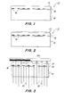
- Fig. 1 is a cross-sectional view of one embodiment of an imaging member 11 in accordance with this invention.
- the imaging member 11 comprises a substrate 13 which is either itself conductive or bears on one surface thereof a conductive film 15. Adjacent the conductive film 15 is disposed photoconductive layer 17.
- the photoconductive layer 17 has incorporated into the surface adjacent the conductive layer 15 an optical screen 19.
- the substrate 13 is of a material transparent to the energy to which the photoreceptor is sensitive.
- the substrate should have a transmissivity to such wavelengths of at least about 50%.
- Any suitable material having these characteristics may be used, such as, for example, Mylar, (trademark) glass, polyethylene, polypropylene, polyvinylfluoride, polycarbonate, polystyrene and the like.
- the general shape of the substrate may take the form of a flat plate, a continuous belt, a cylinder or the like depending upon the design characteristics of the device in which the method in accordance with this invention is to be carried out.
- the substrate must either be conducting in and of itself, or bear on one surface thereof a conductive transparent layer.
- the substrate can be conductive of itself by adding to any of the materials mentioned above suitable conductive particles which will not appreciably effect the transmissivity of the substrate.
- the substrate may be of a polymer which inherently has conductive characteristics such as some polymers known in the art which include within their molecular structure various salt-type groups which render them conductive.
- any suitable conductive material which also has sufficient transparent characteristics may be employed such as, for example, thin layers of metallic substances such as chromium, aluminum, gold, tin, copper, silver and the like. Any suitable thickness of metallic film which permits the transmission of energy to which the photoreceptor is sensitive may be employed. A thickness of from about 1 to about 200 angstroms is generally satisfactory for this purpose.
- a tin oxide, indium oxide layer or a copper iodide layer may be employed.
- a particularly suitable combination is a glass substrate having a tin oxide conductive layer disposed thereon manufactured by Pittsburgh Plate Glass Company under the name "Nesa" glass.
- optical screen 19 Adjacent the conductive layer 15, as shown in Fig. 1, is optical screen 19 and photoreceptor layer 17.
- the optical screen 19, while shown integral with photoreceptive layer 17 in Fig. 1 may comprise a separate layer positioned between the light source 23 (fig 4) and the photoreceptive layer 17 as close as possible to the photoreceptor.
- the optical screen 19 may have any desirable configuration, such as for example, parallel lines, crosshatched parallel lines which form a mesh screen pattern, dots, ellipses, squares, diagonally disposed parallel lines, and the like.
- the optical screen 19 may have a repetitive pattern to form from about 100 to 1,000 lines per lineal inch and preferably from about 250 to about 1,000 lines per lineal inch.
- the optical screen 19 should be such as to form from about 300 to about 500 lines per lineal inch.
- the ratio of transparent areas to opaque areas 0 1 the optical screen will vary from about 20% to about 90%, preferably from about 40% to about 60% and most preferably equal areas of opaque and clear areas will be present.
- the optical screen 19 may be fabricated of any suitable opaque material such as, for example, carbon black, aluminum, copper, gold, silver, chromium and the like.
- the optical screen 19 may be formed by any suitable technique well known in the art such as, for example, silver halide development, photoetching, silk screening, evaporating through a mask, machining and the like.
- a suitable commercially available electroformed copper, nickel or nickel plated copper grid available from C.O. Jelliff Mfg. Corp. under the trademark Lektromesh may be used herein as the optical screen 19. It is preferred that the optical screen 19 have sharply defined transparent and opaque areas and that it be of a reflective material in order to provide for multiple reflections within the photoreceptive material.
- Photoreceptive layer 17 may be fabricated of any suitable material that is both transmissive and sensitive to the wavelength of actinic energy employed to expose the photoreceptor to the information on the document to be reproduced.
- the photoreceptive material should have a transmissivity of from about 20 to about 95%, preferably from about 50 to about 90% of the actinic energy.
- Any suitable material having these characteristics may be employed, such as for example polyvinylcarbazole-trinitrofluorenone in the ratio of about 60:40 percent by weight phthalocyanine and the like.
- a polyvinylcarbazole-trinitrofluorenone (hereinafter referred to as PVK-TNF) in the ratio set forth above has a transmissivity of about 80% and is a preferred material.
- the photoreceptive layer is of a thickness of from about 5 to about 50 microns, preferably from about-10 to about 30 microns and most preferably from about 15 to about 25 microns.
- the photoconductive layer can be of any shape such as a flat plate, belt or drum as indicated above with regard to the substrate and it is preferred that it have a smooth surface in order to facilitate the transfer of the developed image and the cleaning thereof.
- the imaging member of Fig. 1 is uniformly charged by any suitable means well known in the xerographic art, such as, for example corona wire, bias roller, rubbing or the like, to achieve the charge pattern illustrated in Fig. 2.
- Any suitable charging voltage may be employed; however, it is preferred that the charging voltage produces internal fields from about 10 to about 60 volts per micron thickness and preferably from about 15 to about 40 volts per micron thickness of the photoconductive layer.
- the document 25 to be copied is now placed adjacent the free surface of the photoconductive layer 17 as shown in Fig. 3 ) and exposed to a suitable light source.
- the light source may be a point source, a line source or collimated light. Where a noncollimated light source is employed, the spacing between the original document and the photoreceptor should preferably be no greater than four times the cycling period ' of the screen, the period being defined as the distance between two adjacent opaque screen members (i.e. dots, lines, etc.). Because of the divergent nature of the light source the definition of the charge pattern resulting from the exposure will decrease as the distance between the original document and the photoreceptor 17 increases. As shown in Fig.
- the light rays 21 pass sequentially through the substrate 13, the conductive layer 15 and the photoreceptive layer 17 in the clear or open spaces of the screen 19. Where the light rays 21 impinge upon the opaque portions of screen 19, they are prevented from proceeding further into the imaging member.
- the white areas of the original document 25 the light rays are reflected in substantially all directions because of the microscopically rough surface of the document, which is usually paper, and in these white areas the photoconductive layer 17 is uniformly and completely discharged even behind the opaque areas of the optical screen 19.
- the image containing areas of the original document 25 shown as the black portion in Fig. 3, the light rays are substantially completely absorbed.
- the charge on the photoconductive layer 17 immediately behind the opaque areas of the optical screen remains and is present in the form of a periodic charge pattern.
- any suitable method of bringing polar or polarizable toner particles into contact with the periodic charge pattern may be used, such as, for example cascade development, magnetic brush development, powder cloud development, vibrating bed development, fluidized bed development, magnetic microfield donor and the like.
- Single component development is preferred, because two-component developers tend to triboelectrically charge the toner, contributing to background deposition and non-uniform development of the screen pattern of the latent image.
- a magnetic brush formed with magnetic toner only is preferred.
- the toner material must be polar or polarizable. That is, in the presence of the periodic charge pattern, the particles must become polarized in order to be subjected to the force due to the nonuniform field present.
- the toner particles should be of a material having a dielectric constant greater than 2 and a bulk resistivity of at least 10 11 ohm-cm and preferably from about 10 12 ohm-em or greater, there being no practical upper limit.
- Any suitable resinous material having these characteristics and capable of being fixed to the substrate can be employed, such as for example, polyvinyl copolymers, such as polyvinyl acetate, polyvinyl butyral, and the like; polystyrene and copolymers thereof, polyolefins, such as polyethylene, polypropylene and the like; acrylates such as polymethyl acrylate, polymethyl methacrylate, polymethacrylic acid, copolymers thereof and the like, polycarbonates, polyesters resins, epoxy resins and the like.
- the toner particles may have any suitable shape,including spherical, oval, granular, etc. and have a particle size of from about 5 to about 50 microns, preferably about 10 to about 35 microns and most preferably from about 15 to about 30 microns.
- a particularly suitable type of toner materials includes magnetically attractable particles within a resin binder such as those set forth above. The inclusion of the magnetically attractable particles permits the delivery of the toner particles to the periodic charge pattern- without the creation of triboelectric charges on the particles. The method of development should ensure that the toner particles do not become electrostatically charged, because utilizing electrostatically-charged particles limits the maximum density of the copy, particularly in solid areas.
- the developed visible image may be transferred by any suitable well known transfer technique.lincluding electrostatic transfer, pressure transfer, adhesive transfer and the like. Because the toner has no net charge, however, it is necessary to apply charge such as by corona charging prior to using electrostatic transfer to paper or the like. Further, the electrostatic latent image may be initially transferred by known procedures and this charged pattern subsequently developed.
- the image is fixed by any suitable technique, well known in the art, such as for example by heating, by applying solvent or a solvent vapors, pressure or the like.
- the imaging member if necessary, is then cleaned by any suitable technique, for example, fur brush, web cleaning, blade cleaning, magnetic brush or the like. Should the imaging member be fabricated for a single use, then cleaning is not required and it is discarded.
- the optical screen 19 is fabricated of chromium strips applied by evaporation and photoetched to prepare a screen having 1,000 lines per lineal inch and a ratio of clear area to opaque area of 50%.
- the optical screen 19 was applied to a glass substrate having a tin oxide conductive coating thereon.
- the photoreceptive layer 17 is polyvinylcarbazole-trinitrofluorenone in a ratio of 60:40 percent by weight respectively having a thickness of about 13.5 microns.
- This imaging member is positively corona charged in a Xerox (registered trademark) Model D Processor to a surface potential of 300 volts which provides a field of 22 volts per micron.
- the document to be copied is placed onto the flat plate imaging member and exposure is carried out by utilizing a 10 watt light source positioned 10 inches from the imaging member for one second.
- the original document is then removed and the image developed by uitilizing a magnetic brush operating at 0.7 inches per second, with a polarizable toner sold by 3M Company under the trade designation A-09, which has an average number diameter of about 24 microns and an average volume diameter of 36.7 microns, a resistivity of 3 times 10 13 ohm-cm and a dielectric constant of about 3.
- the toner image is transferred from the photoreceptive layer 17 to plain paper by corona charging, then using conventional electrostatic transfer techniques with the opposite polarity and fixed to the paper by fusing.
- the density of the transferred images is exceedingly good and the background exceptionally clean.
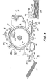
- FIG. 4 schematically depicts the various components of an illustrative electrophotographic printing machine incorporating the present invention therein. It will become evident from the following discussion that the method of this invention described hereinafter is equally well suited for use in a wide variety of electrostatographic printing machines and is not necessarily limited in its application to the particular embodiment shown herein.
- Drum 10 has the cross-sectional configuration shown in Fig. 1.
- Drum 10 rotates in the direction of arrow 12 to pass through the various processing stations disposed thereabout.
- drum 10 moves a portion of the imaging member U through charging station A.
- a corona-generating device indicated generally by the reference numeral 14, charges the photoconductive surface of drum 10 to a relatively high, substantially uniform potential.
- the exposure Station B includes a lamp 23 disposed within the drum 10. The light rays 21, on the initial pass through the imaging member 11 (see Fig. 1) and reflected from the original document, discharge the photoreceptive layer 17 of drum 10 in image configuration to establish on the drum 10 a periodic charge pattern.
- drum 10 advances the electrostatic latent image recorded on the photoconductive surface to development Station C.
- a magnetic brush development system indicated generally by the reference numeral 18, transports a polar or polarizable magnetic toner material as described above, into contact with the photoconductive surface of drum 10.
- the developer material, or a portion thereof, is attracted to the periodic charge pattern latent image forming a toner powder image corresponding to the informational areas of the original document.
- drum 10 advances the powder image to transfer station D.
- sheet-feeding apparatus 20 includes a feed roll 22 contacting the uppermost sheet of the stack 24 of sheets of support material. Feed roll 22 rotates in the direction of arrow 26 so as to advance the uppermost sheet from stack 24. Registration rollers 28, rotating in the direction of arrow 30, align and forward the advancing sheet of support material into chute 32. Chute 32 directs the advancing sheet of support material into contact with the photoconductive surface of drum 10 in a timed sequence. This ensures that the powder image contacts the advancing sheet of support material at transfer station D.
- Transfer station D includes a corona generating device 34, which applies a spray of ions (opposite in polarity to the charged toner) to the backside of the sheet. This attracts the powder image from the photoconductive surface of drum 10 to the sheet. After transfer, the sheet continues to move with drum 10 and is separated therefrom by a detack corona generating device (not shown) which reduces the charge causing the sheet to adhere to the drum. Conveyor 36 advances the sheet, in the direction of arrow 38, from transfer station D to fusing station E.
- Fusing station E indicated generally by the reference numeral 40, includes a back-up roller 42 and a heated fuser roller 44.
- the sheet of support material with the powder image thereon passes between back-up roller 42 and fuser roller 44.
- the powder image contacts fuser roller 44 and the heat and pressure applied thereto permanently bonds it to the sheet of support material.
- a heated pressure system has been described for permanently affixing the particles to a sheet of support material
- a cold pressure system may be utilized in lieu thereof.
- the particular type of fusing system employed depends upon the type of particles being utilized in the development system.
- forwarding rollers 46 advance the finished copy sheet to catch tray 48. Once the copy sheet is positioned in catch tray 48, it may be removed therefrom by the machine operator.
- Cleaning station F includes a cleaning mechanism 50 which may comprise a preclean corona generating device and a rotatably mounted fibrous brush in contact with the photoconductive surface of drum 10.
- the preclean corona generating device neutralizes the charge attracting the particles to the photoconductive surface.
- the particles are then cleaned from the photoconductive surface by the rotation of the brush in contact therewith.
- a discharge lamp floods the photoconductive surface with light to dissipate any residual charge remaining thereon prior to the charging thereof for the next successive imaging cycle.
Landscapes
- Physics & Mathematics (AREA)
- General Physics & Mathematics (AREA)
- Electrophotography Using Other Than Carlson'S Method (AREA)
- Combination Of More Than One Step In Electrophotography (AREA)
Applications Claiming Priority (2)
| Application Number | Priority Date | Filing Date | Title |
|---|---|---|---|
| US13542180A | 1980-03-31 | 1980-03-31 | |
| US135421 | 1987-12-21 |
Publications (2)
| Publication Number | Publication Date |
|---|---|
| EP0037193A2 true EP0037193A2 (fr) | 1981-10-07 |
| EP0037193A3 EP0037193A3 (fr) | 1981-12-30 |
Family
ID=22468032
Family Applications (1)
| Application Number | Title | Priority Date | Filing Date |
|---|---|---|---|
| EP81301014A Withdrawn EP0037193A3 (fr) | 1980-03-31 | 1981-03-11 | Procédé de reprographie électrophotographique |
Country Status (2)
| Country | Link |
|---|---|
| EP (1) | EP0037193A3 (fr) |
| JP (1) | JPS56151954A (fr) |
Family Cites Families (2)
| Publication number | Priority date | Publication date | Assignee | Title |
|---|---|---|---|---|
| US3754965A (en) * | 1971-04-05 | 1973-08-28 | Varian Associates | A method for making an electrophotographic plate |
| DE2718157A1 (de) * | 1977-04-23 | 1978-11-02 | Licentia Gmbh | Verfahren zum herstellen eines elektrophotographischen aufzeichnungsmaterials |
-
1981
- 1981-03-11 EP EP81301014A patent/EP0037193A3/fr not_active Withdrawn
- 1981-03-24 JP JP4308981A patent/JPS56151954A/ja active Pending
Also Published As
| Publication number | Publication date |
|---|---|
| EP0037193A3 (fr) | 1981-12-30 |
| JPS56151954A (en) | 1981-11-25 |
Similar Documents
| Publication | Publication Date | Title |
|---|---|---|
| US4545669A (en) | Low voltage electrophotography with simultaneous photoreceptor charging, exposure and development | |
| US4282303A (en) | Development method and apparatus | |
| US5202206A (en) | Process for simultaneous printing of fixed data and variable data | |
| US4289837A (en) | Development method and apparatus | |
| US3335003A (en) | Reflex xerographic process | |
| US3719481A (en) | Electrostatographic imaging process | |
| US3560205A (en) | Method of forming a phase modulating hologram on a deformable thermoplastic | |
| US3337339A (en) | Screen xerography | |
| GB2095416A (en) | Electrophotographic process and photosensitive member for use in said process | |
| EP0430703B1 (fr) | Procédé d'impression xérographique | |
| US3442645A (en) | Electrophotographic method | |
| US3589290A (en) | Relief imaging plates made by repetitive xerographic processes | |
| EP0120688B1 (fr) | Système de développement utilisant une couche mince de particules de marquage | |
| US4880715A (en) | Imaging system | |
| US4063945A (en) | Electrostatographic imaging method | |
| US3890040A (en) | Induction imaging apparatus | |
| US4572647A (en) | Hybrid development system | |
| US3414409A (en) | Particle transfer | |
| US3166420A (en) | Simultaneous image formation | |
| CA2079609C (fr) | Membre de transfert intermediaire | |
| CA1230915A (fr) | Methode et appareil d'electrophotographie | |
| US3794418A (en) | Imaging system | |
| JPS60103369A (ja) | 現像装置とこれを内蔵する電子写真複写機 | |
| JPH0362272B2 (fr) | ||
| EP0037193A2 (fr) | Procédé de reprographie électrophotographique |
Legal Events
| Date | Code | Title | Description |
|---|---|---|---|
| PUAI | Public reference made under article 153(3) epc to a published international application that has entered the european phase |
Free format text: ORIGINAL CODE: 0009012 |
|
| AK | Designated contracting states |
Designated state(s): DE FR GB |
|
| PUAL | Search report despatched |
Free format text: ORIGINAL CODE: 0009013 |
|
| AK | Designated contracting states |
Designated state(s): DE FR GB |
|
| 17P | Request for examination filed |
Effective date: 19820218 |
|
| STAA | Information on the status of an ep patent application or granted ep patent |
Free format text: STATUS: THE APPLICATION IS DEEMED TO BE WITHDRAWN |
|
| 18D | Application deemed to be withdrawn |
Effective date: 19830331 |
|
| RIN1 | Information on inventor provided before grant (corrected) |
Inventor name: GUNDLACH, ROBERT W. |