EP0037285A2 - Dispositif de mémoire, en particulier circuit amplificateur de ligne de mot pour un dispositif de mémoire - Google Patents
Dispositif de mémoire, en particulier circuit amplificateur de ligne de mot pour un dispositif de mémoire Download PDFInfo
- Publication number
- EP0037285A2 EP0037285A2 EP81301402A EP81301402A EP0037285A2 EP 0037285 A2 EP0037285 A2 EP 0037285A2 EP 81301402 A EP81301402 A EP 81301402A EP 81301402 A EP81301402 A EP 81301402A EP 0037285 A2 EP0037285 A2 EP 0037285A2
- Authority
- EP
- European Patent Office
- Prior art keywords
- word
- transistor
- word line
- power supply
- emitter
- Prior art date
- Legal status (The legal status is an assumption and is not a legal conclusion. Google has not performed a legal analysis and makes no representation as to the accuracy of the status listed.)
- Granted
Links
Images





Classifications
-
- G—PHYSICS
- G11—INFORMATION STORAGE
- G11C—STATIC STORES
- G11C11/00—Digital stores characterised by the use of particular electric or magnetic storage elements; Storage elements therefor
- G11C11/21—Digital stores characterised by the use of particular electric or magnetic storage elements; Storage elements therefor using electric elements
- G11C11/34—Digital stores characterised by the use of particular electric or magnetic storage elements; Storage elements therefor using electric elements using semiconductor devices
- G11C11/40—Digital stores characterised by the use of particular electric or magnetic storage elements; Storage elements therefor using electric elements using semiconductor devices using transistors
- G11C11/41—Digital stores characterised by the use of particular electric or magnetic storage elements; Storage elements therefor using electric elements using semiconductor devices using transistors forming static cells with positive feedback, i.e. cells not needing refreshing or charge regeneration, e.g. bistable multivibrator or Schmitt trigger
- G11C11/413—Auxiliary circuits, e.g. for addressing, decoding, driving, writing, sensing, timing or power reduction
- G11C11/414—Auxiliary circuits, e.g. for addressing, decoding, driving, writing, sensing, timing or power reduction for memory cells of the bipolar type
- G11C11/415—Address circuits
-
- G—PHYSICS
- G11—INFORMATION STORAGE
- G11C—STATIC STORES
- G11C8/00—Arrangements for selecting an address in a digital store
Definitions
- This invention relates to a memory device, more particularly word line drive circuitry for a memory device, for example a random access memory comprising a plurality of memory cells each of which has a flip-flop circuit in which a pair of transistors are cross-connected.
- a random access memory device wherein a plurality of memory cells, each having a basic structure comprising a flip-flop circuit in which a pair of bipolar transistors are cross-connected, are arranged in the form of matrix is generally known as providing a high speed RAM (Random Access Memory).
- Figure 1 shows the general form of a memory cell array in which memory cells MOO ... Mno, ..., Mom ... Mnm are arranged in the form of a (n + 1) x (m + 1) matrix.
- Each memory cell has, as indicated by way of example for cell MOO, a flip-flop circuit wherein the collectors and bases of a pair of bipolar transistors (Qcl, Qc2) are cross-connected.
- WO ... Wn are word lines
- HO ... Hn are hold lines
- BO ... Bm, BO ... Bm are bit lines.
- Word lines WO ... Wn are selected by means of word drivers WDO ... WDn, whilst bit line pairs (BO, BO) ...
- bit drivers BDO ... BDm are selected by bit drivers BDO ... BDm.
- the bit drivers BDO to BDm form current switch circuits in combination with constant current sources IBS.
- a current is applied to only a single pair of bit lines in dependence upon Y selection signals V YO to V Ym . Only one pair of bit lines is selected. It can also be provided that current is applied to all lines.
- a selection is made from amongst word drivers WDO to WDn in dependence upon X selection signals V XO to V Xn so as to make one word line "H" (high) level and to make the remaining word lines "L” (low) level.
- SA is a sense amplifier which forms the detecting system for detecting the contents stored in a memory cell in combination with transistors (Q S10 , Q S20 ) (Q S1m , Q S2m ) for the bit line pairs ((BO, BO) ... (Bm, Bm)).
- the sense amplifier SA has an output OUT and the transistor pairs (Q S10 , Q S20 ) to (Q Slm' Q S2m ) are connected to input lines S, S of SA.
- Constant current sources IH are provided on hold lines HO to Hn.
- Figure 2 shows in more detail a part of Figure 1, while the chart of Figure 3 shows potential relationships of terminals and circuit points indicated in Figure 2.
- the (selected) memory cell M SO (similiar to non-selected cell M NO ) is an emitter detection type cell consisting of a couple of load resistances R L2 Schottky barrier diodes SBD and multi-emitter transistors.
- the transistors Q H1 to Q H4 on the side of hold lines H S , H N , of the multi-emitter transistors of cells M SO , M SN are memory holding transistors, while transistors Q C1 to Q C4 on the side of bit lines Bl, B1 are driver transistors.
- V BS > V CS is obtained between the base voltage V BS of the transistor Q c1 and collector voltage V CS of Q c1 at the time of selection.
- voltage difference (V BS - V CS ) is taken to be V BCS (see Figure 3).
- the base voltage V BS is obtained by subtracting a voltage drop value (which is very small) expressed as the product of load resistance R L of Q c2 and base current of Q c1 from the word line voltage V WS , whilst the collector voltage V CS is obtained by subtracting a value of the forward direction voltage drop (V BE ) of SBD from V cc' because the collector current of Q c1 is sufficiently high so that the diode SBD becomes ON.
- V BE forward direction voltage drop
- V BS becomes low and the flip-flop of M SQ is inverted (not indicated in Figure 3).
- V BS ⁇ V D even if said V D remains at a potential equal to that in read operation, the transistor Q sl becomes ON, whilst transistor Q c1 becomes OFF.
- the.level of V D is generally boosted as indicated in Figure 3 incrder to speed-up the write operation. Therefore, turning to OFF is performed more quickly.
- V WN of the non-selected word line W N must be such that V WN ⁇ V D ( ⁇ V CS ). If the transistor Q H4 of the non-selected memory cell M NO is in ON state at the time of writing operation, the base voltage V BN is almost equal to V WN . If the relationship V WN > V D is established while V D is brought down for write operation, the transistor Q c4 becomes ON and the current I B of the bit line B1 is supplied from the transistor Q c4 . Now, the transistor Q c2 cannot turn sufficently ON or it requires an excessively long period for Q c2 to become ON. In order to avoid such a disadvantage, the relationship V CS > V D > V WN ⁇ V BN must be satisfied.
- the current I B of the bit line Bl is supplied from both transistors Q s2 and Q c4 .
- a difference of currents (I; - I D ) at the sense amplifier SA is reduced by half, and it becomes difficult to read the content of cell M SO .
- Such a disadvantage can be eliminated by changing the level difference between the selected word line and non-selected word line for read and write operations. Moreover, the same effect can be obtained by changing the single selected word line level for read and write operations.
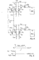
- FIG. 4 is a schematic circuit diagram.
- the circuit shown in Figure 4 includes decoders DEC O to DEC n and word drivers WD 0 to WD n .
- decoders DEC 0 to DEC n only a part thereof is shown.
- transistors (T 10 , T 20 , T30) to (T 1n , T 2n , T 3n ) respectively form current switches
- transistors (T 40 , T 50 ) to (T 4n , T 5n ) respectively form current switches.
- One of decoder signals S 0 to S n becomes low (L) level (S 0 for example) and the transistors (T 10 , T50) become OFF.
- one of the selection signal voltages V XO to V Xn becomes high (H) level.
- one of the word lines WL 0 to WL n becomes H level, namely one word line is selected.
- all of the remaining signals among S 0 to S n become H level, making the relevant transistors (T 10 , T50) to (T 1n , T5n) ON, and resultingly all of the remaining selection signal voltages among V X0 to V Xn become L level, so that the relevant word lines become L level.
- the level of a word line WL 0 to WL n is higher at a time at which the line is selected and it is at the time at which the line is non-selected. However, the selected level is higher during a write operation than it is during a read operation, as shown in Figure 5.
- write control signal WE becomes H during a read operation and becomes L during a write operation.
- the transistor T 20 becomes ON.
- the transistor T 4C becomes ON and a current of current source I X flows through said transistor T 40 , but not through the load resistance R X .
- the circuit shown in Figure 4 must provide current sources I X , I XW for each of the decoders DEC 0 to DEC which are provided for a word drivers WD 0 to WD n ; therefore, the / advantage of a large power consumption appears.
- multi-emitter type transistors are used, together with many other elements, in each of the decoders DEC 0 to DEC n , and therefore, the structure requires is complicated.
- a memory device having an array of memory cells with word lines connected to the memory cells, comprising word drivers, for driving respective word lines of the device, operable to cause the potential of a selected word line to differ from that of a non-selected word line in dependence upon selection signals supplied to input terminals of the respective word drivers from respective word decoders, the word decoders being operable so that the potential of a selection signal supplied to the input terminal of a word driver of a selected word line differs from the potential of a selection signal supplied to the input terminal of a word driver of a non-selected word line, wherein the memory device further comprises a word line selection level switching circuit so connected in common to the word drivers via respective switching parts and so arranged as to cause the potential of a selection signal supplied to the input terminal of a word driver of a selected word line to differ from the potential of a selection signal supplied to the input terminal of a word driver of a non-selected word line by a greater amount in a write operation than in a read operation
- An embodiment of the present invention can provide a RAM device wherein the amplitude of the potential of a word line is changed for write and read operations, so that a high speed read operation and accurate write operation are ensured.
- An embodiment of the present invention can provide a memory array driver circuit wherein non-selected word line voltage is of a constant value and selected word line voltage in write operation is higher than that in read operation.
- An embodiment of the present invention can provide a driver circuit which uses a lesser number of elements, involves a simple circuit structure and provides for lesser power consumption.
- An embodiment of the present invention provides a random access memory device comprising;
- word drivers WD S to WD N provided in correspondence to word lines W s to W N are connected in such a way that a collector of a word driver is connected to a higher voltage power supply V cc , an emitter of a word driver is connected to a word line (W s to W N ) and a base is connected to an input terminal.
- selection signals V XS to V XN are supplied from decoders (not illustrated). Therefore, a high voltage selection signal V XS (H) is supplied to the base of the selected word driver WD S , and the word line W S has thus a high voltage V WS .
- a low voltage selection signal V XN (L) is supplied and thereby the word line W N is kept at a low voltage V WN .
- word line selection level switching circuit SLS is provided.in common to the base points of the input terminals of the word drivers WD S to WD N via switching parts SW S to SW N , respectively.
- the word line selection level switching circuit SLS passes a current I XW from the input terminal of the selected word driver WD S in read operation, in accordance with write control signal WE. Namely, the current I XW flows through the route :- power supply V CC - load resistance R X - switching part; SW S - switching circuit SLS.
- rectifying elements can be used as the switching parts SW S to SW N so that the current I XW is applied from only that selected word driver WD S which has the highest voltage of the input terminals (bases) of the word drivers WD S to WD N .
- read operation selection signal V XS is reduced by R X I XW as compared with that in a write operation.
- amplitude ⁇ R of the difference in potentials of selected and non-selected word lines in a read operation is smaller than the amplitude ⁇ W of the difference in the potentials of selected and non-selected word lines in a write operation.
- ⁇ R is smaller than ⁇ W by R X I XW .
- ⁇ R in a read operation is set to a minimunvalue, the switching time of a selected word line in a read operation becomes short as compared with a conventional time as indicated by ⁇ t of Figure 7. This means that the access time of the RAM is reduced.
- the structure shown in Figure 6 is simpler and consumes less power for several reason.
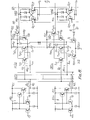
- Figure 8 is a schematic diagram indicating an embodiment of the present invention as'adopted to a logical decoder.
- the decoder DEC S generates signals A O to A and inverted signals A 0 to A m from address inputs A o to A , using address inverters AI 0 to AIm of current switch structure.
- n + 1 decoders DEC 0 to DEC n are provided and address signal groups AG 0 to AG n are provided for the decoders DEC 0 to DEC n respectively.
- Decoder DEC 0 provides a NOR gate composed of transistors T 01 to T 0m , receiving as inputs A 0 to A m , load resistance R X , transistor T OR which forms a current switch together with the NOR gate and a constant current source.
- Selection signal voltage V XO obtained from the decoder DEC Q is applied to an input terminal (base) of a word driver WD 0 (comprising transistor T WO ).
- Further word drivers (WD 1 to WD n ) and decoders are also structured in the same way. Operations are performed as well known. When all of A0 to A m become L level, the transistors T 01 to T 0m become OFF.
- V X (V XO ) becomes equal to V CC and word line W 0 has a selection level.
- current I X flows into load resistance R X
- V x (V XO ) becomes equal to V CC - R X I X and the word line W O has a non-selection level.
- diodes D 0 to D n are provided as rectifying elements of switching parts in order to change the amplitude of the potential of the word lines in read and write operations, and moreover a single word line selection level switching circuit SLS consisting of transistors T 1 and T 2 , and a constant current source I XW is provided in common to the decoders DEC 0 to DEC n .
- the first and second transistors T 1 , T 2 are emitter- connected and the common emitter side is connected to the current source I XW .
- a reference voltage V R is applied to the base of the second transistor T 2 and its collector is connected to a suitable voltage (V CC , for example).
- write control signal WE is applied to the base of the first transistor and its collector is connected in common to the cathodes of diodes D 0 to D n .
- the anodes of diodes D 0 to D n are connected to the points V x (V XO to V XN ) of the word drivers WD 0 to WD n respectively (in Figure 8, V X is as V XS when at a selected level, and as V XN when at a not-selected level).
- V XO is determined by a factor other than I X .
- the write control signal WE is H in a read operation, transistor T 1 becomes ON.
- current I XW flows on the route:-V CC - R X - V XO - D O - T 1 , and V XS (selected level of V XO ) becomes equal to (V CC - R X I XW ) (intermediate value).
- I XW flows from the highest point of V XO to V XN . Therefore, when I X >I XW , V XS is larger than V XN (V XS > V XN ). Thus, I XW flows only into load resistance R X (of the selected decoder DEC 0 ).
- Variation of the potential amplitude of the word lines thus obtained shows a characteristic similar to that obtained conventionally in Figure 5.
- a current switch is formed with rectifying element, diodes D 0 to D n and the word line selection level switching circuit SLS comprising current source I XW and transistors T 1 , T 2 is used in common for all word drivers, thus drastically simplifying circuit structure as compared with the conventional circuit shown in Figure 4 and providing high density integration.
- this embodiment of the invention does not use multi-emitter type transistors and therefore has a simplified circuit pattern and uses fewer current sources, thus consuming less electrical power.
- diodes D 0 to D n are used as the rectifying element of the switching parts.
- any suitable rectifying element can be used.
- a Schottky barrier diode SBD as shown in Figure 9A a transistor TD with base and collector connected as shown in Figure 9B, or a rectifying circuit consisting of resistances R 1 , R 2 and transistor TD' as shown in Figure 9C can also be used.
- Figure 10 is a schematic diagram illustrating another embodiment of the present invention.
- the present invention is adopted to a logical decoder of a type different from that of Figure 8.
- a 0 A 1 , A 0 A 1 , to A 2 A 3 are generated by combining non-inverted and inverted outputs of address inverters AI 0 to AI 3 which receive inputs A 0 to A3.
- a 0 A 1 becomes L level when both A 0 and A 1 are L but becomes H level when any one is H. This is also true of A 0 A 1 to A 2 A 3 .
- Respective pairs of these 2- bit combinations are used as inputs of decoders DEC O to DEC 15 .
- Decoder DEC 0 to which the other decoders are similar, is composed of transistors T 01 , T 02 which are controlled by the inputs A 0 A 1 , A 2 A 3 , load resistance R X , transistors T 05 , T 06 forming a current switch, and a current source I X .
- Word driver WD 0 is composed of a transistor T WO . Operation is the same as in the embodiment of Figure 8. When both A 0 A 1 and A 2 A 3 are L level and transistors T 01 , T 02 become OFF, the transistor T 06 becomes OFF, resulting in V X (V XO ) - V CC . Thus, the word line W O has a selection level.
- diodes D O to D 15 are provided as switching parts at input terminals V XO to V X15 (here selection signals are applied) of the transistors TWO to T W15 of the word drivers WD O to WD 15 and these diodes are connected in common to a single word line selection level switching circuit SLS.
- the operation is the same as Figure 8 and therefore explanation is omitted here.
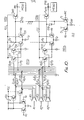
- FIG 11 shows a further embodiment of the present invention employing a general diode matrix type decoder.
- This decoder has current switches CS O to CS m in each of which one transistor receives one of address signals A 0 , A 1 ..., while another transistor receives a reference voltage V R .
- signals A O to A m and inverted signals A 0 to Amcan be obtained.
- desired selections of m + 1 signals from among the 2(m + 1) signals A 0 to A m are connected to the m + 1 emitters of respective multi-emitter transistors of diode matrixes DM O to DM n of decoders DEC O to DECn.
- diodes D O to D n are provided as switching parts connected to input terminals (to which selection signals V XO to V Xn are applied) of driver transistors TW 0 to T Wn of word drivers WD 0 to WD n as in the case of Figure 8, and these diodes are connected in common to one word line selection level switching circuit SLS.
- the operation is the same as that of Figure 8 and therefore explanation is omitted here.
- the word line selection level switching circuit SLS is configurated by a current switch consisting of the transistors T 1 , T 2 and a constant current source I XW , but other circuit configurations can be used.
- Figure 12 shows still another embodiment of the present invention adopted to a logical decoder of the kind seen in Figure 8.
- the word line selection level switching circuit SLS has switching parts comprising diodes D 0 to D n , transistors T 3 , T 4 , T 5 , resistors R 1 , R 2 and R 3 , and diode D'. Respective elements are connected as indicated in Figure 12.
- the collector of transistor T3,and resistor R 2 are connected to a suitable voltage (V CC for example), whilst the diode D', the emitter of transistor T 4 and resistor R 5 are connected to a low voltage.
- the base of transistor T 3 is connected to receive a write control signal WE.
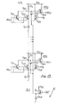
- FIG. 13 is a still further embodiment of the present invention, being adopted to a logical.decoder.
- switching parts comprising diodes D 0 to D n and word line selection level switching circuit SLS consisting of transistor T 6 and constant current source I XW are provided. Connections are as indicated in the Figure.
- the base of transistor T 6 is connected to receive an inverted write control signal WE, namely WE.
- WE is L level and the transistor T 6 turns OFF and thereby the current I XW flows from the highest voltage of the selection signal voltages V XO to V XN*
- WE achieves a sufficiently high level and current I XW flows into the transistor T 6 in the ON state.
- this embodiment can also be adopted to the diode matrix type decoder.
- an embodiment of the present invention can provide a circuit which changes the amplitude of the potential of a word line for write and read operations, and parricularly provides a driver circuit of a memory cell array of a simple circuit structure, which facilitates realization of high speed read and accurate write operation by making the selected word line potential higher during write operation than during read operation, while the potential of non-selected word lines is kept at a constant value. Therefore, a reduction in the number of elements required makes possible higher integration density or pattern simplification and, moreover, reduction in current sources brings about less power consumption. This represents real advantage.
- a random access memory device embodying the present invention has a memory cell matrix array comprising a plurality of memory cells each having a flip-flop circuit wherein a pair of transistors are cross-connected and has word driver transistors provided in correspondence to a plurality of word lines of the memory device.
- Each word driver transistor has its collector connected to a high power supply voltage and its emitter connected to a word line.
- the bases of the word driver transistors are connected in common to a word line selection level switching circuit via respective diodes.
- the word line selection level switching circuit supplies a current in write operation to the common connecting point of diodes and forms a current switch together with the diodes.
- the voltage of a selected word line in write operation is lower than that in read operation.
- An embodiment of the present invention can offer a random access memory device which has a simplified structure, consumes less current and assures high speed read operation.
Landscapes
- Engineering & Computer Science (AREA)
- Microelectronics & Electronic Packaging (AREA)
- Computer Hardware Design (AREA)
- Static Random-Access Memory (AREA)
Applications Claiming Priority (2)
| Application Number | Priority Date | Filing Date | Title |
|---|---|---|---|
| JP55042489A JPS598913B2 (ja) | 1980-04-01 | 1980-04-01 | 記憶装置 |
| JP42489/80 | 1980-04-01 |
Publications (3)
| Publication Number | Publication Date |
|---|---|
| EP0037285A2 true EP0037285A2 (fr) | 1981-10-07 |
| EP0037285A3 EP0037285A3 (en) | 1983-05-18 |
| EP0037285B1 EP0037285B1 (fr) | 1988-06-08 |
Family
ID=12637468
Family Applications (1)
| Application Number | Title | Priority Date | Filing Date |
|---|---|---|---|
| EP81301402A Expired EP0037285B1 (fr) | 1980-04-01 | 1981-03-31 | Dispositif de mémoire, en particulier circuit amplificateur de ligne de mot pour un dispositif de mémoire |
Country Status (5)
| Country | Link |
|---|---|
| US (1) | US4536860A (fr) |
| EP (1) | EP0037285B1 (fr) |
| JP (1) | JPS598913B2 (fr) |
| DE (1) | DE3176784D1 (fr) |
| IE (1) | IE54461B1 (fr) |
Cited By (1)
| Publication number | Priority date | Publication date | Assignee | Title |
|---|---|---|---|---|
| EP0399240A3 (fr) * | 1989-05-20 | 1991-07-03 | Kabushiki Kaisha Toshiba | Dispositif de mémoire à semi-conducteur |
Families Citing this family (4)
| Publication number | Priority date | Publication date | Assignee | Title |
|---|---|---|---|---|
| JPS61104394A (ja) * | 1984-10-22 | 1986-05-22 | Mitsubishi Electric Corp | 半導体記憶装置 |
| US4730275A (en) * | 1985-11-22 | 1988-03-08 | Motorola, Inc. | Circuit for reducing the row select voltage swing in a memory array |
| JPH0442495A (ja) * | 1990-06-07 | 1992-02-13 | Mitsubishi Electric Corp | 半導体記憶装置 |
| US6452858B1 (en) * | 1999-11-05 | 2002-09-17 | Hitachi, Ltd. | Semiconductor device |
Family Cites Families (5)
| Publication number | Priority date | Publication date | Assignee | Title |
|---|---|---|---|---|
| US3541531A (en) * | 1967-02-07 | 1970-11-17 | Bell Telephone Labor Inc | Semiconductive memory array wherein operating power is supplied via information paths |
| US3703711A (en) * | 1971-01-04 | 1972-11-21 | Honeywell Inf Systems | Memory cell with voltage limiting at transistor control terminals |
| JPS5736670B2 (fr) * | 1974-04-24 | 1982-08-05 | ||
| US3986178A (en) * | 1975-07-28 | 1976-10-12 | Texas Instruments | Integrated injection logic random access memory |
| JPS5833634B2 (ja) * | 1979-02-28 | 1983-07-21 | 富士通株式会社 | メモリセルアレイの駆動方式 |
-
1980
- 1980-04-01 JP JP55042489A patent/JPS598913B2/ja not_active Expired
-
1981
- 1981-03-31 EP EP81301402A patent/EP0037285B1/fr not_active Expired
- 1981-03-31 DE DE8181301402T patent/DE3176784D1/de not_active Expired
- 1981-04-01 IE IE748/81A patent/IE54461B1/en unknown
-
1984
- 1984-01-06 US US06/568,952 patent/US4536860A/en not_active Expired - Fee Related
Cited By (2)
| Publication number | Priority date | Publication date | Assignee | Title |
|---|---|---|---|---|
| EP0399240A3 (fr) * | 1989-05-20 | 1991-07-03 | Kabushiki Kaisha Toshiba | Dispositif de mémoire à semi-conducteur |
| US5119337A (en) * | 1989-05-20 | 1992-06-02 | Kabushiki Kaisha Toshiba | Semiconductor memory device having burn-in test function |
Also Published As
| Publication number | Publication date |
|---|---|
| JPS56140586A (en) | 1981-11-02 |
| IE54461B1 (en) | 1989-10-25 |
| IE810748L (en) | 1981-10-01 |
| JPS598913B2 (ja) | 1984-02-28 |
| DE3176784D1 (en) | 1988-07-14 |
| US4536860A (en) | 1985-08-20 |
| EP0037285A3 (en) | 1983-05-18 |
| EP0037285B1 (fr) | 1988-06-08 |
Similar Documents
| Publication | Publication Date | Title |
|---|---|---|
| US4125877A (en) | Dual port random access memory storage cell | |
| US3675218A (en) | Independent read-write monolithic memory array | |
| US4193127A (en) | Simultaneous read/write cell | |
| EP0297571B1 (fr) | Mémoire aléatoire extensible à multi-accès | |
| US4156941A (en) | High speed semiconductor memory | |
| EP0031488A2 (fr) | Cellule de mémoire et son application dans un système de mémoire utilisant une matrice à accès aléatoire | |
| US4348747A (en) | System for driving bipolar ram | |
| US4369503A (en) | Decoder circuit | |
| US4164791A (en) | Semiconductor memory with equal word line and reference line voltage drop | |
| EP0023792A2 (fr) | Mémoire à semi-conducteurs comprenant des cellules intégrées à injection logique | |
| EP0025316A2 (fr) | Circuit de fin de ligne de mot pour dispositif de mémoire à semi-conducteurs | |
| EP0024894A1 (fr) | Circuit de décodage | |
| US4122548A (en) | Memory storage array with restore circuit | |
| US3781828A (en) | Three-dimensionally addressed memory | |
| EP0037285B1 (fr) | Dispositif de mémoire, en particulier circuit amplificateur de ligne de mot pour un dispositif de mémoire | |
| US4464735A (en) | Semiconductor memory | |
| EP0202892B1 (fr) | Dispositif de mémoire à semi-conducteur avec décodeur matriciel à diode et configuration de redondance | |
| EP0182305A2 (fr) | Mémoire morte | |
| JPH0217876B2 (fr) | ||
| EP0078223B1 (fr) | Cellule de mémoire translinéaire alimentée par une ligne de bit | |
| EP0082961A2 (fr) | Réseau de mémoire à accès aléatoire | |
| EP0117646B1 (fr) | Dispositif de mémoire semi-conductrice avec un circuit de commande à lecture-écriture | |
| JPS6037555B2 (ja) | メモリ装置 | |
| US4592023A (en) | Latch for storing a data bit and a store incorporating said latch | |
| US4298961A (en) | Bipolar memory circuit |
Legal Events
| Date | Code | Title | Description |
|---|---|---|---|
| PUAI | Public reference made under article 153(3) epc to a published international application that has entered the european phase |
Free format text: ORIGINAL CODE: 0009012 |
|
| AK | Designated contracting states |
Designated state(s): DE FR GB NL |
|
| RBV | Designated contracting states (corrected) |
Designated state(s): DE FR GB NL |
|
| PUAL | Search report despatched |
Free format text: ORIGINAL CODE: 0009013 |
|
| RHK1 | Main classification (correction) |
Ipc: G11C 11/40 |
|
| AK | Designated contracting states |
Designated state(s): DE FR GB NL |
|
| 17P | Request for examination filed |
Effective date: 19831109 |
|
| GRAA | (expected) grant |
Free format text: ORIGINAL CODE: 0009210 |
|
| AK | Designated contracting states |
Kind code of ref document: B1 Designated state(s): DE FR GB |
|
| REF | Corresponds to: |
Ref document number: 3176784 Country of ref document: DE Date of ref document: 19880714 |
|
| ET | Fr: translation filed | ||
| PLBE | No opposition filed within time limit |
Free format text: ORIGINAL CODE: 0009261 |
|
| STAA | Information on the status of an ep patent application or granted ep patent |
Free format text: STATUS: NO OPPOSITION FILED WITHIN TIME LIMIT |
|
| 26N | No opposition filed | ||
| PGFP | Annual fee paid to national office [announced via postgrant information from national office to epo] |
Ref country code: GB Payment date: 19910215 Year of fee payment: 11 |
|
| PGFP | Annual fee paid to national office [announced via postgrant information from national office to epo] |
Ref country code: FR Payment date: 19910328 Year of fee payment: 11 |
|
| PG25 | Lapsed in a contracting state [announced via postgrant information from national office to epo] |
Ref country code: GB Effective date: 19920331 |
|
| GBPC | Gb: european patent ceased through non-payment of renewal fee | ||
| PG25 | Lapsed in a contracting state [announced via postgrant information from national office to epo] |
Ref country code: FR Effective date: 19921130 |
|
| REG | Reference to a national code |
Ref country code: FR Ref legal event code: ST |
|
| PGFP | Annual fee paid to national office [announced via postgrant information from national office to epo] |
Ref country code: DE Payment date: 19930521 Year of fee payment: 13 |
|
| PG25 | Lapsed in a contracting state [announced via postgrant information from national office to epo] |
Ref country code: DE Effective date: 19941201 |