EP0037301A2 - Verkapselungsgehäuse für Leistungsmodul in Hybridschaltung - Google Patents
Verkapselungsgehäuse für Leistungsmodul in Hybridschaltung Download PDFInfo
- Publication number
- EP0037301A2 EP0037301A2 EP81400393A EP81400393A EP0037301A2 EP 0037301 A2 EP0037301 A2 EP 0037301A2 EP 81400393 A EP81400393 A EP 81400393A EP 81400393 A EP81400393 A EP 81400393A EP 0037301 A2 EP0037301 A2 EP 0037301A2
- Authority
- EP
- European Patent Office
- Prior art keywords
- substrate
- cover
- box according
- hybrid circuit
- encapsulation box
- Prior art date
- Legal status (The legal status is an assumption and is not a legal conclusion. Google has not performed a legal analysis and makes no representation as to the accuracy of the status listed.)
- Granted
Links
Images


Classifications
-
- H—ELECTRICITY
- H10—SEMICONDUCTOR DEVICES; ELECTRIC SOLID-STATE DEVICES NOT OTHERWISE PROVIDED FOR
- H10W—GENERIC PACKAGES, INTERCONNECTIONS, CONNECTORS OR OTHER CONSTRUCTIONAL DETAILS OF DEVICES COVERED BY CLASS H10
- H10W72/00—Interconnections or connectors in packages
-
- H—ELECTRICITY
- H10—SEMICONDUCTOR DEVICES; ELECTRIC SOLID-STATE DEVICES NOT OTHERWISE PROVIDED FOR
- H10W—GENERIC PACKAGES, INTERCONNECTIONS, CONNECTORS OR OTHER CONSTRUCTIONAL DETAILS OF DEVICES COVERED BY CLASS H10
- H10W40/00—Arrangements for thermal protection or thermal control
- H10W40/10—Arrangements for heating
-
- H—ELECTRICITY
- H10—SEMICONDUCTOR DEVICES; ELECTRIC SOLID-STATE DEVICES NOT OTHERWISE PROVIDED FOR
- H10W—GENERIC PACKAGES, INTERCONNECTIONS, CONNECTORS OR OTHER CONSTRUCTIONAL DETAILS OF DEVICES COVERED BY CLASS H10
- H10W40/00—Arrangements for thermal protection or thermal control
- H10W40/60—Securing means for detachable heating or cooling arrangements, e.g. clamps
- H10W40/611—Bolts or screws
-
- H—ELECTRICITY
- H10—SEMICONDUCTOR DEVICES; ELECTRIC SOLID-STATE DEVICES NOT OTHERWISE PROVIDED FOR
- H10W—GENERIC PACKAGES, INTERCONNECTIONS, CONNECTORS OR OTHER CONSTRUCTIONAL DETAILS OF DEVICES COVERED BY CLASS H10
- H10W70/00—Package substrates; Interposers; Redistribution layers [RDL]
- H10W70/60—Insulating or insulated package substrates; Interposers; Redistribution layers
- H10W70/67—Insulating or insulated package substrates; Interposers; Redistribution layers characterised by their insulating layers or insulating parts
- H10W70/69—Insulating materials thereof
- H10W70/692—Ceramics or glasses
-
- H—ELECTRICITY
- H10—SEMICONDUCTOR DEVICES; ELECTRIC SOLID-STATE DEVICES NOT OTHERWISE PROVIDED FOR
- H10W—GENERIC PACKAGES, INTERCONNECTIONS, CONNECTORS OR OTHER CONSTRUCTIONAL DETAILS OF DEVICES COVERED BY CLASS H10
- H10W72/00—Interconnections or connectors in packages
- H10W72/30—Die-attach connectors
-
- H—ELECTRICITY
- H10—SEMICONDUCTOR DEVICES; ELECTRIC SOLID-STATE DEVICES NOT OTHERWISE PROVIDED FOR
- H10W—GENERIC PACKAGES, INTERCONNECTIONS, CONNECTORS OR OTHER CONSTRUCTIONAL DETAILS OF DEVICES COVERED BY CLASS H10
- H10W90/00—Package configurations
-
- H—ELECTRICITY
- H10—SEMICONDUCTOR DEVICES; ELECTRIC SOLID-STATE DEVICES NOT OTHERWISE PROVIDED FOR
- H10W—GENERIC PACKAGES, INTERCONNECTIONS, CONNECTORS OR OTHER CONSTRUCTIONAL DETAILS OF DEVICES COVERED BY CLASS H10
- H10W40/00—Arrangements for thermal protection or thermal control
- H10W40/20—Arrangements for cooling
- H10W40/231—Arrangements for cooling characterised by their places of attachment or cooling paths
- H10W40/235—Arrangements for cooling characterised by their places of attachment or cooling paths attached to package parts
Definitions
- the invention relates to an encapsulation box for a power module produced using hybrid circuit technology. It relates more particularly to an assembly architecture, which comprises new means of power connections and to means for evacuating the heat released by the module as well as to the housing itself which is adapted to these new means.
- hybrid power circuits are not entirely satisfactory since the maximum power according to current technologies is limited.
- Either the hybrid circuits are produced on a single substrate, and the maximum power is limited by the fact that the use of conventional hybrid technology for the elements. control (alumina substrate, integration of thick film resistors, soldering of components at 180 ° C) is not compatible with mounting at 300 ° C and no longer necessary for power pads.
- Either the hybrid circuits are split into a control part on a substrate, and a power part whose components are each mounted in its power box such as for example the boxes of so-called power diodes. D04 or the power transistor boxes called T03. But the fact that the circuit has been split into a part on a substrate and one or more power components in their own housing, it is no longer strictly speaking, a hybrid circuit, and we lose a lot in integration.
- the architecture of the power module according to the invention comprises a single flat substrate on which the signal components and the power components which form the circuit are grouped, and which is closed by a concave cover made of a ceramic material such as alumina.
- the power connections are ensured by pins, supporting an intensity of several amperes, which pass through the cover in which they are sealed, while the calories released by the power components are evacuated directly by a radiator on which the substrate is fixed in thermal coupling via a distributor which has a dual thermal and mechanical function.
- the invention relates to an encapsulation box for a power module, in a hybrid circuit, comprising a planar substrate, on which the components of the hybrid circuit are fixed, and a cover, characterized in that, apart, the external connections of the circuit are constituted by pins, of dimensions able to support the passage of a current which can exceed ten amperes, welded on the circuit, and directed perpendicular to the substrate, and which pass, through holes, through the cover, and on the other hand in that the substrate is fixed, in thermal coupling, on a distributor, ensuring the functions thermal and mechanical interface with a heat exchanger.
- FIG. 1 very schematically represents a conventional hybrid circuit.
- a flat substrate 1 generally made up of a plate of alumina, ceramic, glass or enamelled sheet, are fixed a certain number of components 2 which are active components, transistors, integrated circuits, and passive components, diodes, resistances, capacities.
- FIG. 2 represents a medium power hybrid circuit according to the known art. Like the previous one, it includes a number of active and passive components 2 supported by a substrate plate 1, but the connections with the external circuits are ensured by means of a plug-in connector.
- This plug-in connector comprises, maintained by a rigid insulating part 4, one or two pins 5 which are mainly used for guiding, and an adequate number of pins 6 which are used for the electrical connection with the rest of the circuit.
- the output pins 6 of the medium power hybrid circuit of FIG. 2 are larger and can if necessary evacuate a small number of calories. However, the power released by this type of circuit is still very limited.
- FIG. 3 represents an encapsulation box according to the known art for medium power hybrid circuits. This case is seen from its underside. It comprises a base 7 consisting of a thick metal plate, which essentially serves to evacuate the calories released by the hybrid circuit. Through this base 7, pass, sealed by glass beads, a number of output pins 8 which allow the passage of a certain intensity.
- a box which has the dimensions of a box of a power transistor, has the disadvantage of being limited in volume and of not admitting a hybrid circuit of large area; consequently, it is less and less used in view of the increase in complexity and the dimensions of current hybrid circuits.
- the housing is closed by a cover 9 which is electrically welded to the base 7, which prevents any subsequent interventions or adjustments after the electric welding.
- Such a box can therefore only correspond to an average dissipated power, all other things being equal and with regard to the powers that could currently be dissipated if one had adequate boxes.
- the figure represents a view in space of an encapsulation box for a power module which solves both the problem of connections for high currents, that is to say several amperes per connection, as well as the problem of the dissipation of calories corresponding to a strong power.
- the housing represented by FIG. 4 has a substantially square shape but this is in no way limiting since any other shape adapted to the circuit design or to the configuration of the system to be produced, such as a shape which would be round for example, enters the field of the invention.
- this housing comprises a cavity, sealed and sealed, which protects the components of the hybrid circuit proper.
- This box therefore consists of a flat substrate 10, made of ceramic, but more generally of an electrical insulating material having a good coefficient of heat transfer such as beryllium oxide, boron nitride or sapphire.
- a concave cover 11 On this flat substrate 10 is welded a concave cover 11, the depth of which corresponds to that of the elements arranged in the hybrid circuit.
- the output connections are constituted by pins 12, the diameter of which makes it possible to convey intensities of several amperes, that is to say, for example ten amperes.
- These metal pins 12 pass through the cover of the housing and are held by metallizations 13 which ensure their welding.
- the substrate 10 is also joined in thermal coupling with a metal base (14) (Cu, Al ...) to facilitate the fixing of the micro-component on a radiator element which is here represented in the form of a radiator element with cast aluminum fins, but which can also consist of a part of the chassis of the more complex electronic system, which dissipates heat.
- the housing thus briefly described in this figure, and which will be explained in more detail on the occasion of the following figures, provides a solution to a number of problems.
- One of the current problems with power boxes is that of the cover 11, also called the cover.
- Hybrid circuits dissipating powers of the order of several tens of watts are currently relatively uncommon because of the problems which have been mentioned previously.
- Their use is developed mainly in military or space or professional equipment, that is to say that the number of such cases manufactured is relatively small compared to the series of consumer equipment, and that, very often, such hybrid power circuits are made on demand. Consequently, the production of hoods such as those made of metal is quite expensive, for small series.
- the solution adopted under the invention is both economical, accepted by military or space standards, and easy to implement: it involves making covers 11 or covers made of ceramic material such as alumina which are easily implemented for small series, are electrically insulating and of sufficient thickness so that the sealing at 13 of the output pins 12 is effective and not very fragile.
- FIG. 5 represents a partial section of a power box according to the invention.
- Pin 12 is electrically connected to the patch of power component 15, such as a diode or transistor, by means of a conductive tab 16.
- the electrical and thermal chain from pin 12 to distributor 14, not shown in this figure, which is in thermal coupling with substrate 10, is composed of a part relating to the power components 15, and a part relative to the output pin 12.
- the power component 15 is welded to the substrate 10 by means of a thick layer metallization 17 deposited on the substrate and a preform 18 which ensures the welding between component and thick metallization.
- the active component 15 is also joined to the output pin 12 by means of a metallic and conductive tab 16 on which it is welded by means of a second solder preform 18.
- the pin outlet 12 is welded in its lower part to the substrate 10 by means of a second thick metallization 17; but the metallic conductive tab 16 being sandwiched between the thick metallization 17 and the lower part of the pin 12, between two other solder preforms 18.
- the pin 12 is made integral with the substrate 10 on the one hand, the component of power 15 is also made integral with substrate 10 else part, and a metal tab 16 provides the connection between the two.
- the metal tab consists not of a wire as is generally the case for semiconductors, but of a metal strip whose section allows the passage of several amps.
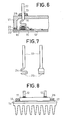
- FIG. 6 represents a sectional view of part of the housing according to the invention, this sectional view making it possible to highlight three details in the welds.
- the box is composed of a substrate 10 and a cover 11. Inside the box, various components are fixed forming a hybrid circuit in the details of which we will not enter.
- the output pin 12 which passes through the cover 11 of the housing, through a hole 19 is fixed by welding. This welding is carried out when the hybrid circuit in its power box is finished, by fusion of a welding preform 13 on a metallized area 20, which welding area had been previously made on the cover.
- the dimensions and the machining precision are sufficient and allow the metallized area 20 to be sufficiently close to the spindle 12, so that the weld preform 13, by melting, wets the spindle 12 without flowing through the hole 19.
- the case is closed by a tin-lead solder under an atmosphere of hydrogenated nitrogen, which makes it airtight and meets the most stringent standards for military or space equipment.
- the cover 11 is metallized on its part 21 which comes into contact with the substrate 10 when these two parts are brought together, the substrate 10 itself being metallized on its corresponding part 22.
- the housing is closed by means of a soft solder preform 23 by reflow in a hydrogen furnace in an atmosphere hydrogenated nitrogen. This closure, which takes place simultaneously with the welding of the outlet connections 12 by means of the preforms 13, seals the housing at the joint between these two main parts and at the outlet connections.
- the method of closing in an oven in a slightly reducing atmosphere simultaneously ensures that the hybrid circuit is sealed in a housing which is itself filled with a neutral atmosphere of nitrogen and hydrogen.
- Figure 6 also shows another method of internal connection to the housing according to the invention. While in FIG. 5, the pin 12 was soldered to the substrate 10, next to the component 15 to which it was connected by a metal tab 16 capable of withstanding a high current, the component 15, is, in FIG. 6. , soldered between the substrate 10 and the pin 12.
- a sandwich structure makes it possible to reduce the contact resistances and to increase the current carried, all the more since it corresponds to the shortest path between an external connection pin 12 and the substrate 10, through which the heat is dissipated.
- This type of mounting is completed by a metal tab 16, sandwiched between the pin 12 and the component 15, and which establishes contact with the rest of the hybrid circuit.
- FIG. 7 represents a front and side view of one of the outlet connections of the housing according to the invention.
- Such an output pin made of copper or of a conductive material, comprises a linear part 12 with a diameter of the order of 1 mm, that is to say much larger than the connections made at the output of the circuits. standard hybrids.
- This linear part 12 is extended, on the side of the connection which is inside the housing according to the invention, by a part of which the metal has first been flattened as shown in the front view, then then bent one or more times, as shown in 24 in the side view, so as to give this metallic part a some flexibility so that it exerts pressure on the metallization or on the component against which it is welded.
- the end of the flexible part 24 of this connection comprises a flat 25 whose edges are chamfered, this flat being the part of the connection pin which is welded to the components and its chamfer being intended not to injure the surface layers of the active components.
- Figure 8 shows an elevational view of a housing according to the invention fixed on a radiator.
- the entire housing is fixed by its substrate 10 to a thermal distributor 14 which is itself mounted on a radiator shown here in the form of a fin radiator.
- a thermal distributor 14 which is itself mounted on a radiator shown here in the form of a fin radiator.
- the shape of this radiator is not limiting of the invention, the important thing being that the radiator has sufficient surface area and calorific mass to absorb the calories released through the oxide substrate. of berylur 14 and dissipate them.
- This radiator can therefore be a part such as the chassis or the body containing an electronic device much more complex than the single hybrid circuit box described.
- the housing can be fixed by two nuts 26 provided with elastic washers so as not to break the substrate during tightening.
- a second method of fixing consists of a layer of adhesive 27 placed between the substrate and the radiator: in this case, it is necessary to provide that the adhesive does not constitute a heat shield. That is why, in some cases it is preferable to replace the adhesive layer 27 with a layer of silicone grease for example, which transmits heat fairly well, and to join the housing and the radiator by means of a number of clips which enclose them both around their perimeter.
- the electronic device such as, for example, the low-voltage switching power supply or inverter, thus encapsulated in a power box according to the invention, constitutes what is called a macro-component in the sense that it forms a whole which receives a certain supply voltage, delivers a current or a voltage meeting precise specifications and that it is autonomous with regard to the dissipated power.
Landscapes
- Cooling Or The Like Of Semiconductors Or Solid State Devices (AREA)
- Wire Bonding (AREA)
Applications Claiming Priority (2)
| Application Number | Priority Date | Filing Date | Title |
|---|---|---|---|
| FR8006689 | 1980-03-26 | ||
| FR8006689A FR2479564A1 (fr) | 1980-03-26 | 1980-03-26 | Boitier d'encapsulation pour module de puissance en circuit hybride |
Publications (3)
| Publication Number | Publication Date |
|---|---|
| EP0037301A2 true EP0037301A2 (de) | 1981-10-07 |
| EP0037301A3 EP0037301A3 (en) | 1981-10-14 |
| EP0037301B1 EP0037301B1 (de) | 1984-05-16 |
Family
ID=9240116
Family Applications (1)
| Application Number | Title | Priority Date | Filing Date |
|---|---|---|---|
| EP81400393A Expired EP0037301B1 (de) | 1980-03-26 | 1981-03-13 | Verkapselungsgehäuse für Leistungsmodul in Hybridschaltung |
Country Status (4)
| Country | Link |
|---|---|
| EP (1) | EP0037301B1 (de) |
| JP (1) | JPS5717156A (de) |
| DE (1) | DE3163581D1 (de) |
| FR (1) | FR2479564A1 (de) |
Cited By (11)
| Publication number | Priority date | Publication date | Assignee | Title |
|---|---|---|---|---|
| EP0098028A3 (de) * | 1982-06-25 | 1985-09-18 | National Aeronautics And Space Administration | Hermetisch versiegelbare Packung für elektronische Hybrid-Festkörperanordnungen und ähnliche Anordnungen |
| DE3505086A1 (de) * | 1985-02-14 | 1986-08-28 | Brown, Boveri & Cie Ag, 6800 Mannheim | Leistungshalbleitermodul mit einem kunststoffgehaeuse |
| FR2618629A1 (fr) * | 1987-07-23 | 1989-01-27 | Telecommunications Sa | Boitier hermetique pour circuit electronique hybride |
| WO1991011824A1 (en) * | 1990-01-24 | 1991-08-08 | Nauchno-Proizvodstvenny Tsentr Elektronnoi Mikrotekhnologii Akademii Nauk Sssr | Three-dimensional electronic unit and method of construction |
| ES2078171A2 (es) * | 1993-12-28 | 1995-12-01 | Smartpack Tecnologia S A | Procedimiento de fabricacion de modulos de potencia con elementos semiconductores. |
| EP0834923A1 (de) * | 1996-10-07 | 1998-04-08 | Gec Alsthom Transport Sa | Elektronik-Halbleiterleistungsmodul und Leistungsunterbrecher damit |
| EP0885459A1 (de) * | 1996-10-16 | 1998-12-23 | Alcatel | Elektronisches leistungsmodul und elektronisches leistungssystem mit einer vielzahl von diesem modul |
| DE102004035746B4 (de) * | 2004-07-23 | 2009-04-16 | Infineon Technologies Ag | Leistungshalbleitermodul |
| DE102013102829B4 (de) * | 2013-03-20 | 2017-10-19 | Semikron Elektronik Gmbh & Co. Kg | Leistungshalbleitermodul und Anordnung hiermit |
| RU2688035C1 (ru) * | 2018-05-14 | 2019-05-17 | Акционерное общество "Научно-производственное предприятие "Пульсар" | Металлокерамический корпус силового полупроводникового модуля на основе высокотеплопроводной керамики и способ его изготовления |
| CN115955802A (zh) * | 2022-12-26 | 2023-04-11 | 深圳市振华微电子有限公司 | 一种一体化多层全密封外壳 |
Families Citing this family (9)
| Publication number | Priority date | Publication date | Assignee | Title |
|---|---|---|---|---|
| JPS59177951A (ja) * | 1983-03-29 | 1984-10-08 | Toshiba Corp | 半導体装置 |
| JPS59208736A (ja) * | 1983-05-12 | 1984-11-27 | Fuji Electric Co Ltd | 半導体装置の組立て方法 |
| JPS6221253A (ja) * | 1985-07-22 | 1987-01-29 | Mitsubishi Electric Corp | パワ−モジユ−ル |
| JPS62127168A (ja) * | 1985-11-28 | 1987-06-09 | Nippon Steel Corp | 交流矩形波プラズマア−ク溶接方法およびその装置 |
| JPH0729670Y2 (ja) * | 1988-10-19 | 1995-07-05 | ティーディーケイ株式会社 | 電源装置 |
| DE102010062556A1 (de) * | 2010-12-07 | 2012-06-14 | Semikron Elektronik Gmbh & Co. Kg | Halbleiterschaltungsanordnung |
| DE102019205411A1 (de) * | 2019-04-15 | 2020-10-15 | Volkswagen Aktiengesellschaft | Halbleiteranordnung |
| CN114068429B (zh) * | 2021-11-10 | 2025-06-03 | 中国电子科技集团公司第四十四研究所 | 宽温高耐压光电隔离开关封装结构及封装方法 |
| CN119517865B (zh) * | 2025-01-14 | 2025-04-11 | 大连宗益科技发展有限公司 | 一种SiC功率器件散热型陶瓷封装结构 |
Family Cites Families (4)
| Publication number | Priority date | Publication date | Assignee | Title |
|---|---|---|---|---|
| GB1085094A (en) * | 1964-04-28 | 1967-09-27 | Lucas Industries Ltd | Alternators |
| FR1535282A (fr) * | 1966-08-29 | 1968-08-02 | C K D Praha Op | Corps de refroidissement pour éléments de construction semi-conducteurs |
| US4000509A (en) * | 1975-03-31 | 1976-12-28 | International Business Machines Corporation | High density air cooled wafer package having improved thermal dissipation |
| US4151547A (en) * | 1977-09-07 | 1979-04-24 | General Electric Company | Arrangement for heat transfer between a heat source and a heat sink |
-
1980
- 1980-03-26 FR FR8006689A patent/FR2479564A1/fr active Granted
-
1981
- 1981-03-13 EP EP81400393A patent/EP0037301B1/de not_active Expired
- 1981-03-13 DE DE8181400393T patent/DE3163581D1/de not_active Expired
- 1981-03-26 JP JP4464081A patent/JPS5717156A/ja active Pending
Cited By (13)
| Publication number | Priority date | Publication date | Assignee | Title |
|---|---|---|---|---|
| EP0098028A3 (de) * | 1982-06-25 | 1985-09-18 | National Aeronautics And Space Administration | Hermetisch versiegelbare Packung für elektronische Hybrid-Festkörperanordnungen und ähnliche Anordnungen |
| US4750031A (en) * | 1982-06-25 | 1988-06-07 | The United States Of America As Represented By The United States National Aeronautics And Space Administration | Hermetically sealable package for hybrid solid-state electronic devices and the like |
| DE3505086A1 (de) * | 1985-02-14 | 1986-08-28 | Brown, Boveri & Cie Ag, 6800 Mannheim | Leistungshalbleitermodul mit einem kunststoffgehaeuse |
| FR2618629A1 (fr) * | 1987-07-23 | 1989-01-27 | Telecommunications Sa | Boitier hermetique pour circuit electronique hybride |
| WO1991011824A1 (en) * | 1990-01-24 | 1991-08-08 | Nauchno-Proizvodstvenny Tsentr Elektronnoi Mikrotekhnologii Akademii Nauk Sssr | Three-dimensional electronic unit and method of construction |
| ES2078171A2 (es) * | 1993-12-28 | 1995-12-01 | Smartpack Tecnologia S A | Procedimiento de fabricacion de modulos de potencia con elementos semiconductores. |
| EP0834923A1 (de) * | 1996-10-07 | 1998-04-08 | Gec Alsthom Transport Sa | Elektronik-Halbleiterleistungsmodul und Leistungsunterbrecher damit |
| FR2754390A1 (fr) * | 1996-10-07 | 1998-04-10 | Gec Alsthom Transport Sa | Module de puissance a composants electroniques semi-conducteurs de puissance et interrupteur de forte puissance comportant au moins un tel module de puissance |
| EP0885459A1 (de) * | 1996-10-16 | 1998-12-23 | Alcatel | Elektronisches leistungsmodul und elektronisches leistungssystem mit einer vielzahl von diesem modul |
| DE102004035746B4 (de) * | 2004-07-23 | 2009-04-16 | Infineon Technologies Ag | Leistungshalbleitermodul |
| DE102013102829B4 (de) * | 2013-03-20 | 2017-10-19 | Semikron Elektronik Gmbh & Co. Kg | Leistungshalbleitermodul und Anordnung hiermit |
| RU2688035C1 (ru) * | 2018-05-14 | 2019-05-17 | Акционерное общество "Научно-производственное предприятие "Пульсар" | Металлокерамический корпус силового полупроводникового модуля на основе высокотеплопроводной керамики и способ его изготовления |
| CN115955802A (zh) * | 2022-12-26 | 2023-04-11 | 深圳市振华微电子有限公司 | 一种一体化多层全密封外壳 |
Also Published As
| Publication number | Publication date |
|---|---|
| DE3163581D1 (en) | 1984-06-20 |
| EP0037301B1 (de) | 1984-05-16 |
| FR2479564B1 (de) | 1983-11-04 |
| FR2479564A1 (fr) | 1981-10-02 |
| JPS5717156A (en) | 1982-01-28 |
| EP0037301A3 (en) | 1981-10-14 |
Similar Documents
| Publication | Publication Date | Title |
|---|---|---|
| EP0037301B1 (de) | Verkapselungsgehäuse für Leistungsmodul in Hybridschaltung | |
| CA1297595C (fr) | Circuit imprime equipe d'un drain thermique | |
| FR2631166A1 (fr) | Boitier de puissance du type a grille de broches pour un circuit integre | |
| FR2813440A1 (fr) | Dispositif a semiconducteur pour la commande d'energie electrique | |
| EP0306412A1 (de) | Gehäuse für elektronische Schaltung | |
| FR2567324A1 (fr) | Dispositif de montage, pour composant hybride a couche epaisse notamment pour module electronique | |
| EP1005089A1 (de) | Leistungshalbleiter | |
| FR2967845A1 (fr) | Architecture de modules electroniques de puissance interconnectes pour une machine electrique tournante et machine electrique tournante comprenant une telle architecture | |
| FR2596608A1 (fr) | Structure de montage et de protection mecanique pour une puce de circuit integre | |
| FR2735648A1 (fr) | Procede de refroidissement d'un circuit integre monte dans un boitier | |
| EP2850658A1 (de) | Strommodulanordnung | |
| FR2779867A1 (fr) | Structure de montage et procede de montage d'un dispositif a semi-conducteur | |
| EP0291400B1 (de) | Leistungsmodul für Fahrzeuganlagen | |
| EP1454516B1 (de) | Energiemodul und energiemodulbaugruppe | |
| FR2500959A1 (fr) | Boitier de dispositif electronique a forte dissipation thermique | |
| EP1079432B1 (de) | Elektronisches Modul und Herstellungsverfahren eines solchen Moduls | |
| FR2693031A1 (fr) | Dispositif à semiconducteurs, substrat et cadre de montage pour ce dispositif. | |
| EP0085622B1 (de) | Montierungsträger für integriertes Schaltungsgehäuse mit Ausgangsleiter verteilt um die äussere Begrenzung des Gehäuses | |
| EP0446125A1 (de) | Leistungshalbleiteranordnung | |
| EP1035573A1 (de) | Elektrisches Leistungsbauelement auf einen Träger gelötet und Montierungsverfahren dafür | |
| FR2758908A1 (fr) | Boitier d'encapsulation hyperfrequences bas cout | |
| WO2003096414A2 (fr) | Assemblage de composants de puissance sur un circuit imprime ainsi qu'un procede d'un tel assemblage | |
| EP0094869B1 (de) | Verkapselungsgehäuse für mikroelektronische Schaltung mit hoher Wärmeabfuhr, und Verfahren zur Herstellung desselben | |
| FR3116944A1 (fr) | Boîtier de circuit integre | |
| FR2829661A1 (fr) | Module de composants electroniques de puissance et procede d'assemblage d'un tel module |
Legal Events
| Date | Code | Title | Description |
|---|---|---|---|
| PUAI | Public reference made under article 153(3) epc to a published international application that has entered the european phase |
Free format text: ORIGINAL CODE: 0009012 |
|
| PUAL | Search report despatched |
Free format text: ORIGINAL CODE: 0009013 |
|
| AK | Designated contracting states |
Designated state(s): BE DE GB IT SE |
|
| AK | Designated contracting states |
Designated state(s): BE DE GB IT SE |
|
| 17P | Request for examination filed |
Effective date: 19811021 |
|
| RAP1 | Party data changed (applicant data changed or rights of an application transferred) |
Owner name: COMPAGNIE D'INFORMATIQUE MILITAIRE SPATIALE ET AE Owner name: THOMSON-CSF |
|
| ITF | It: translation for a ep patent filed | ||
| GRAA | (expected) grant |
Free format text: ORIGINAL CODE: 0009210 |
|
| AK | Designated contracting states |
Designated state(s): BE DE GB IT SE |
|
| REF | Corresponds to: |
Ref document number: 3163581 Country of ref document: DE Date of ref document: 19840620 |
|
| PLBE | No opposition filed within time limit |
Free format text: ORIGINAL CODE: 0009261 |
|
| STAA | Information on the status of an ep patent application or granted ep patent |
Free format text: STATUS: NO OPPOSITION FILED WITHIN TIME LIMIT |
|
| 26N | No opposition filed | ||
| PG25 | Lapsed in a contracting state [announced via postgrant information from national office to epo] |
Ref country code: SE Effective date: 19860314 |
|
| PG25 | Lapsed in a contracting state [announced via postgrant information from national office to epo] |
Ref country code: BE Effective date: 19860331 |
|
| BERE | Be: lapsed |
Owner name: CIE D'INFORMATIQUE MILITAIRE SPATIALE ET AERONAUT Effective date: 19860331 Owner name: THOMSON-CSF Effective date: 19860331 |
|
| GBPC | Gb: european patent ceased through non-payment of renewal fee | ||
| PG25 | Lapsed in a contracting state [announced via postgrant information from national office to epo] |
Ref country code: DE Effective date: 19861202 |
|
| PG25 | Lapsed in a contracting state [announced via postgrant information from national office to epo] |
Ref country code: GB Effective date: 19881118 |
|
| EUG | Se: european patent has lapsed |
Ref document number: 81400393.5 Effective date: 19870224 |