EP0040032A1 - Herstellung eines Halbleiterbauelementes - Google Patents
Herstellung eines Halbleiterbauelementes Download PDFInfo
- Publication number
- EP0040032A1 EP0040032A1 EP81301960A EP81301960A EP0040032A1 EP 0040032 A1 EP0040032 A1 EP 0040032A1 EP 81301960 A EP81301960 A EP 81301960A EP 81301960 A EP81301960 A EP 81301960A EP 0040032 A1 EP0040032 A1 EP 0040032A1
- Authority
- EP
- European Patent Office
- Prior art keywords
- layer
- impurity
- semiconductor layer
- substrate
- semiconductor
- Prior art date
- Legal status (The legal status is an assumption and is not a legal conclusion. Google has not performed a legal analysis and makes no representation as to the accuracy of the status listed.)
- Granted
Links
Images




Classifications
-
- H—ELECTRICITY
- H10—SEMICONDUCTOR DEVICES; ELECTRIC SOLID-STATE DEVICES NOT OTHERWISE PROVIDED FOR
- H10P—GENERIC PROCESSES OR APPARATUS FOR THE MANUFACTURE OR TREATMENT OF DEVICES COVERED BY CLASS H10
- H10P34/00—Irradiation with electromagnetic or particle radiation of wafers, substrates or parts of devices
- H10P34/40—Irradiation with electromagnetic or particle radiation of wafers, substrates or parts of devices with high-energy radiation
- H10P34/42—Irradiation with electromagnetic or particle radiation of wafers, substrates or parts of devices with high-energy radiation with electromagnetic radiation, e.g. laser annealing
-
- H—ELECTRICITY
- H10—SEMICONDUCTOR DEVICES; ELECTRIC SOLID-STATE DEVICES NOT OTHERWISE PROVIDED FOR
- H10D—INORGANIC ELECTRIC SEMICONDUCTOR DEVICES
- H10D64/00—Electrodes of devices having potential barriers
- H10D64/01—Manufacture or treatment
- H10D64/011—Manufacture or treatment of electrodes ohmically coupled to a semiconductor
- H10D64/0111—Manufacture or treatment of electrodes ohmically coupled to a semiconductor to Group IV semiconductors
- H10D64/0113—Manufacture or treatment of electrodes ohmically coupled to a semiconductor to Group IV semiconductors the conductive layers comprising highly doped semiconductor materials, e.g. polysilicon layers or amorphous silicon layers
-
- H—ELECTRICITY
- H10—SEMICONDUCTOR DEVICES; ELECTRIC SOLID-STATE DEVICES NOT OTHERWISE PROVIDED FOR
- H10P—GENERIC PROCESSES OR APPARATUS FOR THE MANUFACTURE OR TREATMENT OF DEVICES COVERED BY CLASS H10
- H10P32/00—Diffusion of dopants within, into or out of wafers, substrates or parts of devices
-
- H—ELECTRICITY
- H10—SEMICONDUCTOR DEVICES; ELECTRIC SOLID-STATE DEVICES NOT OTHERWISE PROVIDED FOR
- H10P—GENERIC PROCESSES OR APPARATUS FOR THE MANUFACTURE OR TREATMENT OF DEVICES COVERED BY CLASS H10
- H10P32/00—Diffusion of dopants within, into or out of wafers, substrates or parts of devices
- H10P32/10—Diffusion of dopants within, into or out of semiconductor bodies or layers
- H10P32/14—Diffusion of dopants within, into or out of semiconductor bodies or layers within a single semiconductor body or layer in a solid phase; between different semiconductor bodies or layers, both in a solid phase
- H10P32/1408—Diffusion of dopants within, into or out of semiconductor bodies or layers within a single semiconductor body or layer in a solid phase; between different semiconductor bodies or layers, both in a solid phase from or through or into an external applied layer, e.g. photoresist or nitride layers
- H10P32/1414—Diffusion of dopants within, into or out of semiconductor bodies or layers within a single semiconductor body or layer in a solid phase; between different semiconductor bodies or layers, both in a solid phase from or through or into an external applied layer, e.g. photoresist or nitride layers the applied layer being silicon, silicide or SIPOS, e.g. polysilicon or porous silicon
-
- H—ELECTRICITY
- H10—SEMICONDUCTOR DEVICES; ELECTRIC SOLID-STATE DEVICES NOT OTHERWISE PROVIDED FOR
- H10P—GENERIC PROCESSES OR APPARATUS FOR THE MANUFACTURE OR TREATMENT OF DEVICES COVERED BY CLASS H10
- H10P32/00—Diffusion of dopants within, into or out of wafers, substrates or parts of devices
- H10P32/10—Diffusion of dopants within, into or out of semiconductor bodies or layers
- H10P32/17—Diffusion of dopants within, into or out of semiconductor bodies or layers characterised by the semiconductor material
- H10P32/171—Diffusion of dopants within, into or out of semiconductor bodies or layers characterised by the semiconductor material being group IV material
Definitions
- the present invention relates to the manufacture of a semiconductor device, and is concerned with a method of diffusing an impurity in the course of manufacture of a semiconductor device.
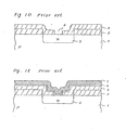
- FIGS 1A to 1E of the accompanying drawings are respective schematic sectional views illustrating a method of diffusing an impurity in which method a phosphosilicate-glass (PSG) film is employed as an insulating film containing an impurity.
- PSG phosphosilicate-glass
- 1 is a p type silicon semiconductor .substrate, whilst 2 is a silicon dioxide (Si0 2 ) film.
- the SiO 2 film 2 is provided with a window at a specified area thereof.
- 3 is a PSG film.
- This PSG film 3 contains about 20% phosphorus and has a thickness of about 1 ⁇ m.
- the semiconductor substrate 1 is annealed for about 20 minutes at a temperature of about 1050 0 C in a nitrogen (N 2 ) atmosphere.
- an ' n type impurity region 5 is formed by diffusion.
- the depth of the region 5 is about 0.4 ⁇ m and its surface resistance ⁇ s is about 20 ⁇ /square.
- a window 6 is formed as shown in Figure ID.
- an aluminium layer (Al) 7 is ordinarily used to provide a contact electrode for region 5.
- Al aluminium layer
- steps are taken for obtaining an ohmic contact between the region 5 and the Al layer 7 provided on the semiconductor substrate, a status change into an alloy of the Al and Si sometimes proceeds abnormally, with a result that the shallow pn junction formed in the semiconductor substrate 1 is destroyed. Therefore, there is employed a method in which a thin polycrystalline silicon layer 4 is formed on the exposed silicon substrate surface before Al layer 7 is formed, and then after formation of the Al layer 7 on the layer 4, the Al and Si are alloyed.
- a thermal process for providing roundness (rounded edges) for the window in the PSG layer 3 is carried out in advance in order to prevent disconnection or discontinuity of the Al layer 7.
- an impurity diffusion method utilizing an insulation film containing an impurity to be diffused involves a variety of processes, and moreover requires that a variety of factors to be taken into account to provide for the leading out of a low resistance contact electrode from the impurity diffused region (5) formed in the semiconductor substrate.
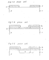
- Figures 2A to 2C are respective schematic sectional views illustrating an impurity diffusion method in which a polycrystalline silicon layer is used as a semiconductor layer containing an impurity.
- 11 is a p type silicon semiconductor substrate; 12 is a silicon dioxide film; 17 is a polycrystalline silicon layer.
- poly-Si layer 17 The thickness of polycrystalline silicon (poly-Si) layer 17 is about 0.4 ⁇ m.
- This poly-Si of the layer may contain an impurity (e.g. phosphorus) at the time of formation of the layer or a non-doped poly-Si layer may be formed initially and impurity (e.g. phosphorus) introduced subsequently.
- impurity e.g. phosphorus
- annealing is carried out for about 20 minutes at a temperature of about 1050°C in a N 2 atmosphere.
- a n type impurity region 15 is formed by diffusion, as indicated in Figure 2B.
- the depth of the impurity region 15 at its centre is about 0.4 ⁇ m, but its depth at parts thereof around the edges of the window in Si0 2 film 12 is about 0.7 to 0.8 ⁇ m as indicated by 18 in Figure 2B.
- This deeply diffused impurity region 18 is usually called the "Dragon teeth” and is believed to be generated as an effect of causes explained hereunder.
- the impurity diffusion method utilising poly-Si it is possible to execute diffusion processes, and thereafter to carry out patterning of the remaining poly-Si layer and to use the poly-Si layer directly as wiring.
- the surface resistance is comparatively large, being about 50 to 70 ⁇ /square.
- a contact electrode can be led rather easily from the diffused region (15) and the process for providing the contact electrode is simplified.
- 19 is an Al electrode. To obtain an ohmic contact between the electrode 19 and the n type impurity diffusion region 15 it is required only to alloy the poly-Si layer 17 used for the impurity diffusion and the Al layer 19.
- a method of manufacturing a semiconductor device comprising:-
- An embodiment of the present invention can provide for the upgrading of element characteristics through the provision of an impurity diffusion of uniform depth, by diffusion of an impurity from a semiconductor layer containing the impurity into a semiconductor substrate.
- An embodiment of the present invention can make it possible to extract a contact electrode having a low resistance from an impurity diffusion region formed in a semiconductor substrate.
- An embodiment of the present invention can provide for a reduced resistance value of a contact electrode provided from an impurity diffusion region formed in a semiconductor substrate and can improve element characteristics.
- an embodiment of the present invention provides an impurity diffusion method comprising the steps of:-
- the semiconductor layer containing an impurity may contain an impurity when it is formed, or the impurity may be introduced into the layer.after formation.
- the semiconductor layer may be a polycrystalline semiconductor layer or amorphous semiconductor layer.
- the semi- conductor layer containing an impurity is irradiated with a high energy beam, and a single-crystalline semiconductor layer is consequently left on the substrate and is used as a contact electrode extending from an impurity diffusion region.
- a portion of the semiconductor layer and substrate is melted when irradiated by a high energy beam and an impurity diffusion region having uniform depth is momentarily formed through impurity diffusion. Simultaneously, an ohmic contact having a low resistance is obtained between the semiconductor layer and the impurity diffusion region. Additionally, the semiconductor layer is single-crystallised and is directly used as the contact electrode having a low resistance.
- 21 is a p type silicon substrate the main surface of which is a (100) surface, whilst 22 indicates a resist film formed as a mask.
- Antimony (Sb) ions are implanted through the substrate surface at an energy of 100 KeV and a dose amount of 1 x 10 15 c m- 2 . Then, after removing the resist film 22, a silicon dioxide film (not shown) is formed on the substrate surface. Thereafter, annealing is carried out for about 70 minutes at a temperature of 1200°C in a dry N 2 ambient in order to activate the implanted ions.
- an n type epitaxial silicon layer is formed on the substrate to a thickness of about 1.5 ⁇ m.
- 30 is an n type buried portion, having a conductivity type determined by the activated Sb ions, whilst 31 is an n type epitaxial silicon layer formed through thermal decomposition of monosilane (SiH 4 ). At the time of formation of the epitaxial layer 31, P 2 O 5 is mixed into the reaction gas and thereby n type conductivity is provided.
- a silicon dioxide film is formed on the epitaxial layer 31, to a thickness of about 500 ⁇ , by a thermal oxidation process, and then a silicon nitride (Si 3 N 4 ) film 32 is formed to a thickness of about 100 ⁇ by an ordinary CVD (Chemical Vapour Deposition) method, sequentially (not illustrated).
- CVD Chemical Vapour Deposition
- etching of the exposed silicon surface through a thickness of about 0.8 ⁇ m is carried out using potassium hydroxide (KOH) as etching solution.
- KOH potassium hydroxide
- the silicon epitaxial layer 31 has a surface (100) as its main surface and a tapered groove is formed by anisotropic etching using the KOH.
- Boron ions are implanted through the surface of layer 31 using the silicon nitride film 32 and silicon oxide film as a mask.
- the dose amount is 1 x 10 13 c m- 2 and the energy is 50 KeV.
- the implanted ions are activated by a thermal process carried out in a wet 0 2 atmosphere and the silicon dioxide layer is caused to grow in the said groove to such a thickness as to provide a substantially flat surface.
- 33, 34 are p type regions provided with that conductivity type by the activated boron ions, and 35 is the thick silicon dioxide film.
- a resist film (not shown) is selectively formed on the surface (the upper surface in Figure 3D). Then, boron ions are implanted using the resist film as a mask with a dose amount of 1 x 10 14 cm -2 and an energy of 100 KeV.
- a thermal process is carried out in an N 2 atmosphere in order to activate the implanted ions and thereby a p type base region is formed.
- 36 indicates the p type base region.
- a poly-Si layer is formed to a thickness of about 0.4 ⁇ m over the entire (upper) surface and then an Si 3 N 4 film of a thickness of about 500 A is formed, sequentially.
- 136 is the poly-Si layer, whilst 37 is the Si 3 N 4 film.
- etching through a thickness of about 0.2 ⁇ m is carried out selectively for the poly-Si layer 136 using the remaining parts of the Si 3 N 4 film 37 as a mask.
- One groove 38 formed by this etching of the poly-Si layer 136 is formed on tbebase region 36, whilst another groove 39 bridges over the base region 36 and the (collector) region 31.
- the poly-Si layer 136 is selectively oxidised using the Si 3 N 4 film 37 as a mask.
- 40, 41 are silicon dioxide layers and 42 is a resist film formed as a mask.
- phosphorus ions are implanted using the resist 42 bridging over the silicon oxide films 40, 41 as a mask.
- This ion implantation is carried out with a dose amount of about 5 x 10 16 cm -2 and an energy of about 150 KeV. Therefore, all ions implanted remain in the poly-Si layer 136.
- a mask (not illustrated) consisting of inverted resist 42 is formed and boron ions are implanted. Namely, ions are implanted into the region covered by mask 42 in the preceding step.
- dose amount is about 5 x 10 16 cm -2 and implantation energy is about 50 KeV.
- a laser is used to irradiate the polycrystalline semiconductor layer with a high energy beam.
- the substrate is heated up in advance to 500 °C and a CW Ar laser is used. Moreover, the irradiation with the laser is effected at a scan speed of about 10 cm/sec with a power of 5 W and a spot size of 50 Am.
- the impurity diffusion rate in melted silicon is very high as compared with that in solid silicon and therefore there is no time for generation of lattice defects due to the difference between the thermal expansion coefficients of the silicon dioxide layer and poly-Si layer. Thus the impurity diffusion process is completed.
- a shallow impurity diffusion region having a uniform depth can be obtained without generating abnormal diffusion in parts near to a boundary with insulating film.
- 43, 44 are single-crystallised n type polycrystalline semiconductor layer parts; 45 is a single-crystallised p polycrystalline semiconductor layer part; 46 is an n type emitter region of a depth of about 0.2 ⁇ m; 47 is a p type base contact region of a depth of about 0.2 A m; 48 is an n type collector contact region of a depth of about 0.2 ⁇ m.
- the poly-Si layer 136 is melted and single-crystallised by.irradiation with a laser beam, thus forming the single-crystalline silicon layer parts 43, 44, 45.
- the surface resistance ⁇ s which was about 50 to 70
- J1- /square in the poly-Si layer is reduced to 20 to 30 ⁇ /square by the single-crystallisation.
- 49 is an emitter electrode consisting of an Al layer structure
- 50 is a base electrode consisting of an Al layer structure
- 51 is a collector electrode consisting of an Al layer structure, respectively.
- the semiconductor layer connected to an impurity diffusion region is single-crystallised, it can be used directly as a contact electrode, through patterning thereof, without any problem, and it can also be connected with metal electrodes as required as shown in Figure 3I.
- the shallow pn junction is not destroyed by an alloy of the silicon and the electrode aluminium, and also electrodes can be lead out by a simple process, because the electrodes are not directly connected to impurity diffusion regions.
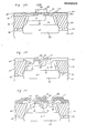
- Figures 4A to 4G illustrate an embodiment of the present invention for the manufacture of a silicon gate type MOS transistor.
- 61 is a p type silicon substrate having a specific resistance of 10 to 20 ⁇ . cm; 62 is a thick silicon dioxide (Si0 2 ) layer for element isolation; 63 is a gate oxide film, as thin as 500 ⁇ , in an element forming area; 64 is a poly-Si layer of a thickness of about 4000 ⁇ .
- Phosphorus ions are implanted from the surface with a dose amount of 4 x 10 16 cm -2 and an energy of 50 KeV. Succeedingly, annealing is carried out for about 20 minutes at a temperature of about 1050°C in a N 2 atmosphere in order to activate the implanted ions.
- the phosphorus doped poly-Si layer 64 and the thin SiO 2 film 63 are etched by an ordinary photo-etching method.
- 65 is a gate electrode consisting of remaining poly-Si layer after etching; and 63 is the gate oxide film remaining under the gate electrode after etching, respectively.
- a poly-Si layer containing an impurity has a high oxidation rate as compared with that of a single-crystalline semiconductor layer.
- the surface of silicon substrate 61 is oxidized to a thickness of about 500 ⁇
- the surface of the gate electrode consisting of phosphorus doped poly-Si layer 64 is oxidised to a thickness of about 4000 ⁇ .
- 66 is an SiO 2 layer formed in such an oxidation process. Such oxidation process is executed at a temperature of about 850°C in a wet 0 2 atmosphere.
- the thin part of oxide film 66 formed on the substrate surface is removed by reactive ion etching using carbon tetrafluoride (CF 4 ) as reaction gas. Even after the substrate surface has been perfectly exposed by this reactive ion etching process, a silicon oxide film thicker than 3000 1 still remains on the gate electrode 65.
- CF 4 carbon tetrafluoride
- a poly-Si layer is formed to a thickness of about 4000 A over the entire exposed (upper) surface by an ordinary CVD method.
- 66 is the silicon oxide layer remaining on the gate electrode, and 67 is the poly-Si layer.
- phosphorus (P) ions or arsenic (As) ions are . implanted through the surface with a dose amount of 4 x 10 16 cm -2 and an energy of about 50 KeV, followed by a process for activation of the implanted ions, carried out in a .N 2 atmosphere.
- impurity diffusion is effected by irradiating the poly-Si layer with a high energy laser beam.
- the substrate is heated up in advance to a temperature of about 500°C, and a CW Ar laser is used to provide the high energy beam.
- a CW Ar laser is used to provide the high energy beam.
- poly-Si layer is irradiated by a laser beam with a power of 5 W, a spot size of about 50 ⁇ m and a scan speed of about 10 cm/sec.
- the poly-Si containing an impurity, and a part of semi-conductor substrate are melted, and impurity diffusion and single-crystallisation of the poly-Si layer are carried out simultaneously.
- 68 is the resulting single-crystallised n type semiconductor layer; and 69, 70 are source and drain regions of a depth of about 0.2 JAm formed by impurity diffusion.
- etching is carried out until at least the silicon oxide film 66 covering the gate electrode is exposed, using an etching solution of HF; HNO 3 ; buffer.
- connection electrode can be connected to an impurity diffusion region with a low resistance, and such a contact electrode itself has a low specific resistance such as 20 to 30 ⁇ /square as compared with a conventional electrode.
- 72 is a silicon dioxide layer obtained by oxidising the surface of single-crystallised semiconductor layer 68; 73 is a PSG film; 74 indicates windows in the PSG film, melted in order to prevent disconnection of Al wiring; 75 is a drain electrode consisting of Al; 76 is a source electrode consisting of Al.
- the present invention allows for the connection of electrodes to take place on the thick oxide film provided for inter-element isolation. This makes it possible very easily to lead out electrodes from the source and drain regions which conventionally would have had to be done in the comparatively narrow area and is also effective for improving production yield.
- embodiment of the present invention provide for the diffusion of an impurity to a uniform depth, from a semiconductor layer containing the impurity into a semiconductor substrate, and also provide for improved element characteristics.
- a contact electrode can be extended with a low resistance from an impurity diffusion region formed inside the semiconductor substrate.
- the resistance value of a contact electrode itself can be reduced and element characteristicscan be improved by single-crystallising the contact electrode.
- the embodiments of the present invention explained above employ-a semiconductor layer which is a polycrystalline semiconductor layer, but alternatively an amorphous semi- conductor layer can be used.
- Embodiments of the present invention can also be realised by irradiating with an Ar laser, a ruby laser, and also with the use of an ion beam, or a photon beam or an electron beam etc., as the high energy beam.
- a shallow uniform impurity diffusion region can beobtained in a semiconductor substrate through the steps of forming an insulating film, having a window therein, on the semiconductor substrate, then forming a semiconductor layer on the insulating film and on the semiconductor substrate exposed in the window, and diffusing a specified impurity from this semiconductor layer into the semiconductor substrate with melting of the semiconductor layer by a high energy beam.
- the melted semiconductor layer is single crystallised and can be used as a contact electrode having a low resistance extending from the impurity diffusion region.
- impurity diffusion into the semiconductor layer which acts as impurity diffusion source may be performed at the time of forming the semi- conductor layer or after the formation of the semiconductor layer.
- the high energy beam it is practical to use a laser beam.
- an embodiment of the present invention provides a method of manufacturing a semiconductor device, comprising:-
- single-crystallisation of the semiconductor layer through the irradiation with the high energy beam can provide a contact electrode of low resistance.
Landscapes
- Electrodes Of Semiconductors (AREA)
- Recrystallisation Techniques (AREA)
Applications Claiming Priority (2)
| Application Number | Priority Date | Filing Date | Title |
|---|---|---|---|
| JP63571/80 | 1980-05-14 | ||
| JP6357180A JPS56160034A (en) | 1980-05-14 | 1980-05-14 | Impurity diffusion |
Publications (2)
| Publication Number | Publication Date |
|---|---|
| EP0040032A1 true EP0040032A1 (de) | 1981-11-18 |
| EP0040032B1 EP0040032B1 (de) | 1983-11-09 |
Family
ID=13233061
Family Applications (1)
| Application Number | Title | Priority Date | Filing Date |
|---|---|---|---|
| EP81301960A Expired EP0040032B1 (de) | 1980-05-14 | 1981-05-05 | Herstellung eines Halbleiterbauelementes |
Country Status (5)
| Country | Link |
|---|---|
| US (1) | US4407060A (de) |
| EP (1) | EP0040032B1 (de) |
| JP (1) | JPS56160034A (de) |
| DE (1) | DE3161362D1 (de) |
| IE (1) | IE51199B1 (de) |
Cited By (3)
| Publication number | Priority date | Publication date | Assignee | Title |
|---|---|---|---|---|
| EP0270703A1 (de) * | 1986-12-12 | 1988-06-15 | Deutsche ITT Industries GmbH | Verfahren zum Herstellen einer monolithisch integrierten Schaltung mit mindestens einem bipolaren Planartransistor |
| EP0252206A3 (en) * | 1986-07-09 | 1988-08-31 | Hitachi, Ltd. | Method of fabricating semiconductor device |
| EP0265958A3 (de) * | 1986-10-30 | 1989-09-27 | SGS Microelettronica SpA | Verfahren zum Herstellen von Feldeffekttransistoren mit isoliertem Gate |
Families Citing this family (22)
| Publication number | Priority date | Publication date | Assignee | Title |
|---|---|---|---|---|
| JPS5946065A (ja) * | 1982-09-09 | 1984-03-15 | Toshiba Corp | 半導体装置の製造方法 |
| US4488348A (en) * | 1983-06-15 | 1984-12-18 | Hewlett-Packard Company | Method for making a self-aligned vertically stacked gate MOS device |
| JPS6057952A (ja) * | 1983-09-09 | 1985-04-03 | Toshiba Corp | 半導体装置の製造方法 |
| JPS6089953A (ja) * | 1983-10-22 | 1985-05-20 | Agency Of Ind Science & Technol | 積層型半導体装置の製造方法 |
| US4510676A (en) * | 1983-12-06 | 1985-04-16 | International Business Machines, Corporation | Method of fabricating a lateral PNP transistor |
| US4735911A (en) * | 1985-12-17 | 1988-04-05 | Siemens Aktiengesellschaft | Process for the simultaneous production of bipolar and complementary MOS transistors on a common silicon substrate |
| US4947225A (en) * | 1986-04-28 | 1990-08-07 | Rockwell International Corporation | Sub-micron devices with method for forming sub-micron contacts |
| US4685199A (en) * | 1986-04-29 | 1987-08-11 | Rca Corporation | Method for forming dielectrically isolated PMOS, NMOS, PNP and NPN transistors on a silicon wafer |
| US4839302A (en) * | 1986-10-13 | 1989-06-13 | Matsushita Electric Industrial Co., Ltd. | Method for fabricating bipolar semiconductor device |
| JPS63182860A (ja) * | 1987-01-26 | 1988-07-28 | Toshiba Corp | 半導体装置とその製造方法 |
| US5051805A (en) * | 1987-07-15 | 1991-09-24 | Rockwell International Corporation | Sub-micron bipolar devices with sub-micron contacts |
| US4929995A (en) * | 1988-02-16 | 1990-05-29 | Honeywell Inc. | Selective integrated circuit interconnection |
| US5217909A (en) * | 1990-07-18 | 1993-06-08 | Siemens Aktiengesellschaft | Method for manufacturing a bipolar transistor |
| JP3315730B2 (ja) * | 1991-08-26 | 2002-08-19 | マイクロリス、コーパレイシャン | ピエゾ抵抗半導体センサ・ゲージ及びこれを作る方法 |
| US5225371A (en) * | 1992-03-17 | 1993-07-06 | The United States Of America As Represented By The Secretary Of The Navy | Laser formation of graded junction devices |
| US6677214B1 (en) * | 1993-11-19 | 2004-01-13 | Mega Chips Corporation | Semiconductor device and method of fabricating the same |
| US5393687A (en) * | 1993-12-16 | 1995-02-28 | Taiwan Semiconductor Manufacturing Company | Method of making buried contact module with multiple poly si layers |
| US6150072A (en) * | 1997-08-22 | 2000-11-21 | Siemens Microelectronics, Inc. | Method of manufacturing a shallow trench isolation structure for a semiconductor device |
| US6535535B1 (en) * | 1999-02-12 | 2003-03-18 | Semiconductor Energy Laboratory Co., Ltd. | Laser irradiation method, laser irradiation apparatus, and semiconductor device |
| US6319743B1 (en) | 1999-04-14 | 2001-11-20 | Mykrolis Corporation | Method of making thin film piezoresistive sensor |
| US6406966B1 (en) * | 2000-11-07 | 2002-06-18 | National Semiconductor Corporation | Uniform emitter formation using selective laser recrystallization |
| US6468871B1 (en) * | 2000-11-07 | 2002-10-22 | National Semiconductor Corporation | Method of forming bipolar transistor salicided emitter using selective laser annealing |
Citations (2)
| Publication number | Priority date | Publication date | Assignee | Title |
|---|---|---|---|---|
| US4181538A (en) * | 1978-09-26 | 1980-01-01 | The United States Of America As Represented By The United States Department Of Energy | Method for making defect-free zone by laser-annealing of doped silicon |
| EP0015677A1 (de) * | 1979-02-28 | 1980-09-17 | Vlsi Technology Research Association | Verfahren zur Herstellung von Halbleitervorrichtungen |
Family Cites Families (11)
| Publication number | Priority date | Publication date | Assignee | Title |
|---|---|---|---|---|
| US3420719A (en) * | 1965-05-27 | 1969-01-07 | Ibm | Method of making semiconductors by laser induced diffusion |
| JPS5816337B2 (ja) * | 1975-06-13 | 1983-03-30 | 日本電気株式会社 | 半導体装置の製造方法 |
| JPS5235983A (en) * | 1975-09-17 | 1977-03-18 | Hitachi Ltd | Manufacturing method of field effective transistor |
| JPS5236468A (en) * | 1975-09-18 | 1977-03-19 | Fujitsu Ltd | Shallow diffusion method |
| FR2340619A1 (fr) * | 1976-02-04 | 1977-09-02 | Radiotechnique Compelec | Perfectionnement au procede de fabrication de dispositifs semiconducteurs et dispositifs ainsi obtenus |
| US4182024A (en) * | 1977-12-15 | 1980-01-08 | National Semiconductor Corporation | Automatic control of integrated circuit trimming |
| US4268950A (en) * | 1978-06-05 | 1981-05-26 | Texas Instruments Incorporated | Post-metal ion implant programmable MOS read only memory |
| US4267011A (en) * | 1978-09-29 | 1981-05-12 | Tokyo Shibaura Denki Kabushiki Kaisha | Method for manufacturing a semiconductor device |
| JPS55138831A (en) * | 1979-04-18 | 1980-10-30 | Hitachi Ltd | Production of semiconductor device |
| JPS5633822A (en) * | 1979-08-29 | 1981-04-04 | Hitachi Ltd | Preparation of semiconductor device |
| JPS56135969A (en) * | 1980-03-27 | 1981-10-23 | Fujitsu Ltd | Manufacture of semiconductor device |
-
1980
- 1980-05-14 JP JP6357180A patent/JPS56160034A/ja active Pending
-
1981
- 1981-05-05 DE DE8181301960T patent/DE3161362D1/de not_active Expired
- 1981-05-05 EP EP81301960A patent/EP0040032B1/de not_active Expired
- 1981-05-06 IE IE996/81A patent/IE51199B1/en not_active IP Right Cessation
- 1981-05-13 US US06/263,281 patent/US4407060A/en not_active Expired - Lifetime
Patent Citations (2)
| Publication number | Priority date | Publication date | Assignee | Title |
|---|---|---|---|---|
| US4181538A (en) * | 1978-09-26 | 1980-01-01 | The United States Of America As Represented By The United States Department Of Energy | Method for making defect-free zone by laser-annealing of doped silicon |
| EP0015677A1 (de) * | 1979-02-28 | 1980-09-17 | Vlsi Technology Research Association | Verfahren zur Herstellung von Halbleitervorrichtungen |
Non-Patent Citations (2)
| Title |
|---|
| IBM Technical Disclosure Bulletin, Vol. 21, No. 10, March 1979 New York R.F. LEVER "Background Heating for Laser Annealing" page 4040 * |
| IBM Technical Disclosure Bulletin, Vol. 22, No. 9, February 1980 New York T.H. YEH "Self-Aligned Intergrated NPN (Vertical) and PNP (Lateral) Structures" pages 4047 to 4051 * page 4048, paragraph 2); page 4051, paragraph 6A), 8A); fig. 2, 6A to 9A * * |
Cited By (4)
| Publication number | Priority date | Publication date | Assignee | Title |
|---|---|---|---|---|
| EP0252206A3 (en) * | 1986-07-09 | 1988-08-31 | Hitachi, Ltd. | Method of fabricating semiconductor device |
| EP0265958A3 (de) * | 1986-10-30 | 1989-09-27 | SGS Microelettronica SpA | Verfahren zum Herstellen von Feldeffekttransistoren mit isoliertem Gate |
| EP0270703A1 (de) * | 1986-12-12 | 1988-06-15 | Deutsche ITT Industries GmbH | Verfahren zum Herstellen einer monolithisch integrierten Schaltung mit mindestens einem bipolaren Planartransistor |
| US4786610A (en) * | 1986-12-12 | 1988-11-22 | Lothar Blossfeld | Method of making a monolithic integrated circuit comprising at least one bipolar planar transistor |
Also Published As
| Publication number | Publication date |
|---|---|
| IE51199B1 (en) | 1986-10-29 |
| IE810996L (en) | 1981-11-14 |
| DE3161362D1 (en) | 1983-12-15 |
| EP0040032B1 (de) | 1983-11-09 |
| US4407060A (en) | 1983-10-04 |
| JPS56160034A (en) | 1981-12-09 |
Similar Documents
| Publication | Publication Date | Title |
|---|---|---|
| EP0040032B1 (de) | Herstellung eines Halbleiterbauelementes | |
| EP0146895B1 (de) | Verfahren zur Herstellung von Halbleiteranordnungen | |
| EP0060613B1 (de) | Verfahren zum Herstellen eines Kontaktlochs für Halbleiterbauelemente | |
| US3913211A (en) | Method of MOS transistor manufacture | |
| US4488351A (en) | Method for manufacturing semiconductor device | |
| EP0139467A1 (de) | Verfahren zum Herstellen eines Feldeffekttransistors mit isoliertem Gate | |
| US4060427A (en) | Method of forming an integrated circuit region through the combination of ion implantation and diffusion steps | |
| US4810665A (en) | Semiconductor device and method of fabrication | |
| US4437225A (en) | Method of forming SOS devices by selective laser treatment and reactive formation of isolation regions | |
| EP0037261A1 (de) | Verfahren zur Herstellung einer Halbleiteranordnung und eine nach diesem Verfahren hergestellte Anordnung, z.B. ein BOMIS FET | |
| JPS6260817B2 (de) | ||
| EP0038178A1 (de) | Verfahren zur Herstellung einer Halbleiteranordnung mit Schottky-Sperrschicht und Vorrichtung | |
| US4408387A (en) | Method for producing a bipolar transistor utilizing an oxidized semiconductor masking layer in conjunction with an anti-oxidation mask | |
| US4465528A (en) | Method of producing a walled emitter semiconductor device | |
| RU1830156C (ru) | Способ изготовлени полупроводниковых приборов | |
| JP2565161B2 (ja) | 半導体装置の製造方法 | |
| JPS6161268B2 (de) | ||
| JP2611252B2 (ja) | 半導体装置の製造方法 | |
| JPH0795535B2 (ja) | 半導体装置の製造方法 | |
| JP3207551B2 (ja) | 半導体装置の製造方法 | |
| JP3224432B2 (ja) | 半導体装置の製造方法 | |
| JP3311082B2 (ja) | 半導体装置の製造方法 | |
| JPH0595000A (ja) | 半導体装置の製造方法 | |
| JPH0126186B2 (de) | ||
| JPH0744183B2 (ja) | 半導体装置の製造方法 |
Legal Events
| Date | Code | Title | Description |
|---|---|---|---|
| PUAI | Public reference made under article 153(3) epc to a published international application that has entered the european phase |
Free format text: ORIGINAL CODE: 0009012 |
|
| AK | Designated contracting states |
Designated state(s): DE FR GB NL |
|
| RBV | Designated contracting states (corrected) |
Designated state(s): DE FR GB NL |
|
| 17P | Request for examination filed |
Effective date: 19820127 |
|
| GRAA | (expected) grant |
Free format text: ORIGINAL CODE: 0009210 |
|
| AK | Designated contracting states |
Designated state(s): DE FR GB NL |
|
| REF | Corresponds to: |
Ref document number: 3161362 Country of ref document: DE Date of ref document: 19831215 |
|
| ET | Fr: translation filed | ||
| PLBE | No opposition filed within time limit |
Free format text: ORIGINAL CODE: 0009261 |
|
| STAA | Information on the status of an ep patent application or granted ep patent |
Free format text: STATUS: NO OPPOSITION FILED WITHIN TIME LIMIT |
|
| 26N | No opposition filed | ||
| PGFP | Annual fee paid to national office [announced via postgrant information from national office to epo] |
Ref country code: GB Payment date: 19950424 Year of fee payment: 15 |
|
| PGFP | Annual fee paid to national office [announced via postgrant information from national office to epo] |
Ref country code: FR Payment date: 19950510 Year of fee payment: 15 |
|
| PGFP | Annual fee paid to national office [announced via postgrant information from national office to epo] |
Ref country code: DE Payment date: 19950511 Year of fee payment: 15 |
|
| PGFP | Annual fee paid to national office [announced via postgrant information from national office to epo] |
Ref country code: NL Payment date: 19950531 Year of fee payment: 15 |
|
| PG25 | Lapsed in a contracting state [announced via postgrant information from national office to epo] |
Ref country code: GB Effective date: 19960505 |
|
| PG25 | Lapsed in a contracting state [announced via postgrant information from national office to epo] |
Ref country code: NL Effective date: 19961201 |
|
| GBPC | Gb: european patent ceased through non-payment of renewal fee |
Effective date: 19960505 |
|
| PG25 | Lapsed in a contracting state [announced via postgrant information from national office to epo] |
Ref country code: FR Effective date: 19970131 |
|
| PG25 | Lapsed in a contracting state [announced via postgrant information from national office to epo] |
Ref country code: DE Effective date: 19970201 |
|
| NLV4 | Nl: lapsed or anulled due to non-payment of the annual fee |
Effective date: 19961201 |
|
| REG | Reference to a national code |
Ref country code: FR Ref legal event code: ST |