EP0040251A1 - Dispositif de memoire a semi-conducteur - Google Patents
Dispositif de memoire a semi-conducteur Download PDFInfo
- Publication number
- EP0040251A1 EP0040251A1 EP80902128A EP80902128A EP0040251A1 EP 0040251 A1 EP0040251 A1 EP 0040251A1 EP 80902128 A EP80902128 A EP 80902128A EP 80902128 A EP80902128 A EP 80902128A EP 0040251 A1 EP0040251 A1 EP 0040251A1
- Authority
- EP
- European Patent Office
- Prior art keywords
- transistor
- read
- memory device
- semiconductor memory
- charge injection
- Prior art date
- Legal status (The legal status is an assumption and is not a legal conclusion. Google has not performed a legal analysis and makes no representation as to the accuracy of the status listed.)
- Granted
Links
Images


Classifications
-
- G—PHYSICS
- G11—INFORMATION STORAGE
- G11C—STATIC STORES
- G11C16/00—Erasable programmable read-only memories
- G11C16/02—Erasable programmable read-only memories electrically programmable
- G11C16/04—Erasable programmable read-only memories electrically programmable using variable threshold transistors, e.g. FAMOS
- G11C16/0408—Erasable programmable read-only memories electrically programmable using variable threshold transistors, e.g. FAMOS comprising cells containing floating gate transistors
- G11C16/0441—Erasable programmable read-only memories electrically programmable using variable threshold transistors, e.g. FAMOS comprising cells containing floating gate transistors comprising cells containing multiple floating gate devices, e.g. separate read-and-write FAMOS transistors with connected floating gates
-
- H—ELECTRICITY
- H03—ELECTRONIC CIRCUITRY
- H03K—PULSE TECHNIQUE
- H03K3/00—Circuits for generating electric pulses; Monostable, bistable or multistable circuits
- H03K3/02—Generators characterised by the type of circuit or by the means used for producing pulses
- H03K3/353—Generators characterised by the type of circuit or by the means used for producing pulses by the use, as active elements, of field-effect transistors with internal or external positive feedback
- H03K3/356—Bistable circuits
- H03K3/356008—Bistable circuits ensuring a predetermined initial state when the supply voltage has been applied; storing the actual state when the supply voltage fails
-
- H—ELECTRICITY
- H10—SEMICONDUCTOR DEVICES; ELECTRIC SOLID-STATE DEVICES NOT OTHERWISE PROVIDED FOR
- H10B—ELECTRONIC MEMORY DEVICES
- H10B69/00—Erasable-and-programmable ROM [EPROM] devices not provided for in groups H10B41/00 - H10B63/00, e.g. ultraviolet erasable-and-programmable ROM [UVEPROM] devices
-
- H—ELECTRICITY
- H10—SEMICONDUCTOR DEVICES; ELECTRIC SOLID-STATE DEVICES NOT OTHERWISE PROVIDED FOR
- H10D—INORGANIC ELECTRIC SEMICONDUCTOR DEVICES
- H10D30/00—Field-effect transistors [FET]
- H10D30/60—Insulated-gate field-effect transistors [IGFET]
-
- H—ELECTRICITY
- H10—SEMICONDUCTOR DEVICES; ELECTRIC SOLID-STATE DEVICES NOT OTHERWISE PROVIDED FOR
- H10D—INORGANIC ELECTRIC SEMICONDUCTOR DEVICES
- H10D30/00—Field-effect transistors [FET]
- H10D30/60—Insulated-gate field-effect transistors [IGFET]
- H10D30/68—Floating-gate IGFETs
- H10D30/681—Floating-gate IGFETs having only two programming levels
- H10D30/684—Floating-gate IGFETs having only two programming levels programmed by hot carrier injection
- H10D30/685—Floating-gate IGFETs having only two programming levels programmed by hot carrier injection from the channel
-
- H—ELECTRICITY
- H10—SEMICONDUCTOR DEVICES; ELECTRIC SOLID-STATE DEVICES NOT OTHERWISE PROVIDED FOR
- H10W—GENERIC PACKAGES, INTERCONNECTIONS, CONNECTORS OR OTHER CONSTRUCTIONAL DETAILS OF DEVICES COVERED BY CLASS H10
- H10W20/00—Interconnections in chips, wafers or substrates
- H10W20/40—Interconnections external to wafers or substrates, e.g. back-end-of-line [BEOL] metallisations or vias connecting to gate electrodes
Definitions
- the present invention relates to a semiconductor memory device composed of the double gate type field effect transistors having the control gate and floating gate for accumulating charges. Moreover, it relates to a semiconductor memory device which assures high charge injection efficiency and also high read-out efficiency.
- FIG. 1 shows the sectional view of the conventional double gate type field effect transistor.
- the structure and operation principle of the transistor of this type are disclosed in the U.S. Patent No. 3,984,822.
- a transistor shown in Fig. 1 provides, on the silicon semiconductor substrate 10 of the one conductivity type (P type), the source region 11 of the opposite conductivity type (N type), drain region 12, electrically floated floating gate 13 and the control gate 15.
- the reference numeral 14 is the insulating layer (silicon oxide), while 16 is the lead-out electrode connected to the source 11 and drain 12. 17 is the high concentration region of the one conductivity type (P type).
- a transistor has a low conductivity or is not conductive when electrons are accumulated in the floating gate 13, or has a high conductivity when electrons are not accumulated.
- Charges can be removed by irrading the transistor with the ultra-violet ray and other electromagnetic waves or a radioactive ray.
- the high concentration region 17 of the conductivity type (P type) same as the substrate 10 is formed on the substrate 10 between the source region 11 and drain region 12. Formation of this high concentration region 17 makes narrower the depletion layer existing in the channel near the drain region at the time of write operation. Therefore, the electrical field in the depletion layer is intensified and resultingly an energy of carrier accelerated in the depletion layer becomes high, also making high the probability of hot carrier generation. As a result, the injection efficiency of hot carrier into the floating gate 13 is improved. This means that the higher write operation lowers the write voltage.
- the read-out operation efficiency is degraded when the high concentration region 17 is provided. Namely, since the channel concentration becomes havy, a threshold voltage becomes high and the conductance gm of a transistor becomes small. Thereby, a high power supply voltage is required in order to increase the read-out voltage to be applied to the control gate 15. Moreover, when the read-out voltage is lowered, a difference between the threshold voltage when no electron is injected to the floating gate 13 and the read-out voltage becomes small, making slow the read-out operation. On the other hand, it is conceivable to widen the channel of transistor in view of making large the conductance gm, but it results in extension of area occupied by a transistor, intending to deterioration of integration density. An attempt of obtaining the high concentration channel is equal to the setting of inconvenient condition for the highly efficient read-out operation.
- a semiconductor memory device having the double gate type field effect transistor of the present invention is provided with the transistor only for charge injection and that only for read-out operation respectively providing the source region and drain region of the opposite conductivity type isolately formed on the substrate surface having the one conductivity type the electrically floated conductive floating gate formed between said source region and drain region on said substrate and the control gate isolated from said floating gate via an insulator, wherein said floating gates of the transistor only for charge injection and that only for read-out operation are connected electrically, said control gate is connected to the first signal line (word line), said drains are connected respectively to the different second and third signal lines (bit lines) and said sources are connected to the same power supply, thus with such a characteristic that both transistors mentioned above are designed with the optimum condition in regard to the impurity concentration of substrate between said source and drain regions and design conditions of each part of said transistors.
- a memory cell provides a transistor only for charge injection and that only for read-out operation so that it can satisfy the conditions of write operation by injecting charges and of read-out operation opposing to it.
- Figure 2 shows a schematic diagram related to an embodiment of the present invention.
- the floating gates 23W, 23R of the transistor T rW only for charge injection and the transistor Tr R only for read-out operation are electrically connected. Therefore, when charges are injected to the floating gate 23W from the transistor T rW , it is also injected to the floating gate 23R of the transistor T rR .
- the control gate 25W of the transistor T rW and the control gate 25R of the transistor T rR are connected in common to the 1st signal line 25, the drain of the transistor T rW is connected to the 2nd signal line 26 while the drain of the transistor T R to the 3rd signal line 27 respectively, and the sources of both transistors T rW , T rR are connected in common.
- Figure 3 outlines the plan view indicating the structure of a memory cell shown in Fig. 2.
- the transistors T rW' T rR have the common floating gate 23.
- the control gate is formed with the 1st signal line 25.
- 22W, 22R are drain regions and 21W, 21R are source regions which are composed of the common diffused layers.
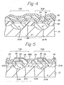
- Figure 4 and Figure 5 show the sectional view along the line A-A' of Fig. 3 and the sectional view along the line B-B'.
- the reference numerals given respective portions of figure are the same as those in Fig. 3.
- 24, 28 are insulating layers.
- the 1st signal line 25 and the floating gate 23 are composed of, for example, the poly-crystal silicon layer, while the insulating layers 24, 28 are composed of, for example, the silicon oxide layer.
- the semiconductor substrate 10 consisting of the silicon has the P type conductivity, while the source regions 21R, 21W and the drain regions 22W, 22R have the N type conductivity.
- Each portion of the transistor T rW only for charge injection and the transistor T rR only for the read-out operation is designed respectively under the optimum condition.
- the high concentration regions 27W, 27R which are higher in the P type impurity concentration than the substrate 10 and the concentration of the region 27W is high and the region 27R is lower than the region 27W in the concentration.
- the transistor T rW only for the charge injection is used.
- the substrate 10 and the source 21W are grounded and a positive high voltage is applied to the 1st signal line 25 and the 2nd signal line 26. Since the high impurity concentration region 27W is provided in the channel of transistor T rW , the probability of generating hot carriers is high and the write efficiency is very excellent.
- the transistor T rW is not required to satisfy the design condition required for the read-out operation opposing to the design condition for the write efficiency, the efficiency of charge injection in the transistor T rW is fantastically excellent as compared with the prior art as mentioned above. Therefore, the write operation is carried out at a high speed.
- the transistor T rR only for the read-out operation is used. First, the substrate 10 and the source 21R are grounded and the specified read-out operation is applied to the 1st signal line 25. As this read-out voltage, an interim voltage between the threshold voltages when the charges are accumulated in the floating gate 23 or not accumulated. Thus, the stored information can be read by detecting a difference of degree of conductivities of transistor T rR due to an existence or not existence of the injected charges of the floating gate 23 through detection of a voltage or current on the 3rd signal line 27 at that time.
- the impurity concentration of the high concentration region 27R of channel of the transistor T rR is lower than that of the region 27W and is also-lower than that of the high concentration region 17 of the conventional transistor explained above.
- the threshold voltage becomes lower and the conductance gm becomes higher. For this reason, the write voltage can be lowered. Moreover, since a difference between the threshold voltage when no electrons are injected and the read-out voltage is larger than that of the prior art even when the read-out voltage is sufficiently low, the high speed read-out operation can be realized.
- the transistor T rW is not required to have a large conductance gm. Resultingly, it is not required to widen the channel width in order to make large the conductance gm, unlike the conventional transistor. Therefore, the area occupied by the transistor T rW can be reduced as compared with the conventional one.
- the transistor T rR has sufficiently low threshold voltage and sufficiently high conductance gm, there is no need of widening the channel which is done in the conventional transistor. As a result, the area occupied by the transistor T rR can also be reduced as compared with the conventional one.
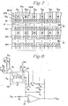
- Figure 6 outlines the schematic diagram indicating the entire part of the semiconductor memory device of an embodiment of the present invention.
- the memory cells MC11, MC12 Vietnamese respectively have the same structure as Figs. 3, 4, 5 described above.
- Figure 7 outlines the plan view indicating the structure of the schematic diagram of Fig. 6.
- the word lines W 1 , W 2 Vietnamese are arranged in parallel to the groove direction, and the hatched portion indicates the floating gate of memory cells being formed by the poly-crystalline silicon layer.
- the portion enclosed by the broken line indicates the area of a single memory cell MC11.
- 22W is the drain region of transistor Q w11
- 22R is the drain region of transistor Q R11
- 21 is the common source region
- 22W, 22R 21 are all composed of the impurity diffused regions provided on the substrate.
- the drain regions 22W and 22R are respectively connected to the bit lines B w1 , B R1 , while the bit lines B W1' B R1 Vietnamese are formed, for example, by the Al layer provided on the word lines W 1 , W 2 .
- the common source region 21 is grounded.
- FIG 8 is the analog invertor circuit related to another embodiment of the present invention.
- the analog invertor circuit receives an input of V IN and provides an polary-inverted output V OUT -V IN .
- the compensating resistors R 21 , R 22' Vietnamese are prepared in parallel to the resistor R 2 and the compensating transistors Q 1 , Q 2 Vietnamese turned ON in accordance with the result of test after completion, thus connecting the resistors R 21 , R 22 , Across in parallel to the resistor R 2 .
- the said compensating transistors Q 1 , Q 2 ?? are turned ON through injection of charges (electrons) into the floating gate of transistors Q R and Q w of the memory cells MC.
- the memory cell MC has almost the same structure as the aforementioned embodiment.
- the charges are injected by the transistor Q W through application of a high voltage to the test terminal V PP and resultingly the transistor Q R is turned OFF setting the terminal N1 to a high voltage level, turning ON the tran- s i s tor Q 1 . If no charge is injected, the transistor Q R is turned ON, setting the terminal N1 to a low voltage level, turning OFF the transistor Q 1 .
- This process is also adopted to the transistors Q2, .
- the transistors Q R , Q W of the memory cell MC can be formed by almost the same process as the other devices having the double poly-crystalline silicon layers, except only for providing the high impurity region in the channel. Therefore, as in the case of this embodiment, even when the memory cell MC is provided within the ordinary circuit other than the memory device wuch as analog circuit, any change of production process is almost not required. Moreover, since the charge injection voltage can be lowered and the read-out voltage can also be lowered, efficiency is so far improved than the case where the memory cell having the conventional structure is used.
- the double gate type field effect transistor which has improved the write efficiency and read-out efficiency by charge injection, and it, as a semiconductor memory device, can be used effectively as the compensating switching circuit in the ordinary circuit such as the analog invertor etc.
Landscapes
- Engineering & Computer Science (AREA)
- Microelectronics & Electronic Packaging (AREA)
- Non-Volatile Memory (AREA)
- Semiconductor Memories (AREA)
- Read Only Memory (AREA)
Abstract
Applications Claiming Priority (2)
| Application Number | Priority Date | Filing Date | Title |
|---|---|---|---|
| JP146167/79 | 1979-11-12 | ||
| JP54146167A JPS5929155B2 (ja) | 1979-11-12 | 1979-11-12 | 半導体記憶装置 |
Publications (3)
| Publication Number | Publication Date |
|---|---|
| EP0040251A1 true EP0040251A1 (fr) | 1981-11-25 |
| EP0040251A4 EP0040251A4 (fr) | 1984-08-10 |
| EP0040251B1 EP0040251B1 (fr) | 1987-05-06 |
Family
ID=15401639
Family Applications (1)
| Application Number | Title | Priority Date | Filing Date |
|---|---|---|---|
| EP80902128A Expired EP0040251B1 (fr) | 1979-11-12 | 1980-11-06 | Dispositif de memoire a semi-conducteur |
Country Status (5)
| Country | Link |
|---|---|
| US (1) | US4403307A (fr) |
| EP (1) | EP0040251B1 (fr) |
| JP (1) | JPS5929155B2 (fr) |
| DE (1) | DE3071967D1 (fr) |
| WO (1) | WO1981001484A1 (fr) |
Cited By (11)
| Publication number | Priority date | Publication date | Assignee | Title |
|---|---|---|---|---|
| EP0085550A3 (en) * | 1982-01-29 | 1986-02-12 | Seeq Technology, Incorporated | Electrically-programmable and electrically-erasable mos memory device |
| WO1988002174A3 (fr) * | 1986-09-22 | 1988-07-28 | Ncr Co | Reseau de cellules de memoire remanentes |
| EP0236676A3 (en) * | 1986-01-14 | 1989-11-02 | Fujitsu Limited | Erasable programmable read only memory using floating gate field effect transistors |
| GB2221343A (en) * | 1988-07-27 | 1990-01-31 | Intel Corp | Semiconductor cell for neural network and the like |
| EP0354859A1 (fr) * | 1988-08-11 | 1990-02-14 | STMicroelectronics S.A. | Mémoire de type eprom à haute densité d'intégration avec une organisation en damier et un facteur de couplage amélioré |
| EP0399261A3 (fr) * | 1989-05-24 | 1991-01-02 | Texas Instruments Incorporated | Injection d'électrons chauds du substrat induite par un transfert de bande à bande |
| EP0534676A3 (en) * | 1991-09-25 | 1993-09-15 | American Telephone And Telegraph Company | Eeprom with improved endurance properties |
| EP0562299A1 (fr) * | 1992-03-24 | 1993-09-29 | International Business Machines Corporation | Structure et méthode de fabrication d'une cellule mémoire EEPROM avec implantations sélectives de canal |
| EP0570257A1 (fr) * | 1992-05-15 | 1993-11-18 | Thomson-Csf | Dispositif semiconducteur à effet de champ avec grille secondaire, procédé de réalisation et application à un dispositif à commande matricielle |
| EP0495492A3 (en) * | 1991-01-17 | 1994-06-01 | Texas Instruments Inc | Non-volatile memory cell structure and process for forming same |
| US8594204B2 (en) | 1995-07-21 | 2013-11-26 | Koninklijke Philips N.V. | Method and device for basic and overlay video information transmission |
Families Citing this family (15)
| Publication number | Priority date | Publication date | Assignee | Title |
|---|---|---|---|---|
| JPS59117270A (ja) * | 1982-12-24 | 1984-07-06 | Mitsubishi Electric Corp | 浮遊ゲ−ト型不揮発性mos半導体メモリ装置 |
| US5262987A (en) * | 1988-11-17 | 1993-11-16 | Seiko Instruments Inc. | Floating gate semiconductor nonvolatile memory having impurity doped regions for low voltage operation |
| US5739569A (en) * | 1991-05-15 | 1998-04-14 | Texas Instruments Incorporated | Non-volatile memory cell with oxide and nitride tunneling layers |
| JPH0575981U (ja) * | 1992-03-18 | 1993-10-15 | 矢崎総業株式会社 | ガラス板用コネクタ |
| US5329487A (en) * | 1993-03-08 | 1994-07-12 | Altera Corporation | Two transistor flash EPROM cell |
| JP4036923B2 (ja) * | 1997-07-17 | 2008-01-23 | 株式会社半導体エネルギー研究所 | 表示装置およびその駆動回路 |
| TW337607B (en) | 1997-08-06 | 1998-08-01 | Mos Electronics Taiwan Inc | Process for forming a contact hole in an EEPROM with NOR construction |
| US6781881B2 (en) * | 2002-12-19 | 2004-08-24 | Taiwan Semiconductor Manufacturing Company | Two-transistor flash cell for large endurance application |
| US7038947B2 (en) * | 2002-12-19 | 2006-05-02 | Taiwan Semiconductor Manufacturing Co., Ltd. | Two-transistor flash cell for large endurance application |
| JP2008257804A (ja) * | 2007-04-05 | 2008-10-23 | Renesas Technology Corp | 半導体装置 |
| KR101553762B1 (ko) | 2011-05-10 | 2015-09-16 | 쌩-고벵 글래스 프랑스 | 전기 연결 요소를 구비한 창유리 |
| MX2013013015A (es) | 2011-05-10 | 2014-01-31 | Saint Gobain | Hoja de vidrio que comprende un elemento de conexion electrica. |
| BR112013028049B1 (pt) | 2011-05-10 | 2020-10-06 | Saint-Gobain Glass France | Painel com pelo menos um elemento de conexão elétrico,método para produção e uso de tal painel |
| PT2896269T (pt) | 2012-09-14 | 2017-06-23 | Saint Gobain | Placa de vidro com um elemento de ligação elétrica |
| MY170325A (en) | 2012-09-14 | 2019-07-17 | Saint Gobain | Pane with an electrical connection element |
Family Cites Families (4)
| Publication number | Priority date | Publication date | Assignee | Title |
|---|---|---|---|---|
| JPS5321837B2 (fr) * | 1973-05-11 | 1978-07-05 | ||
| JPS5716747B2 (fr) * | 1974-10-01 | 1982-04-07 | ||
| DE2723738C2 (de) * | 1977-05-26 | 1984-11-08 | Deutsche Itt Industries Gmbh, 7800 Freiburg | Halbleiterspeicherzelle für das nichtflüchtige Speichern elektrischer Ladung und Verfahren zu deren Programmierung |
| US4257056A (en) * | 1979-06-27 | 1981-03-17 | National Semiconductor Corporation | Electrically erasable read only memory |
-
1979
- 1979-11-12 JP JP54146167A patent/JPS5929155B2/ja not_active Expired
-
1980
- 1980-11-06 US US06/280,008 patent/US4403307A/en not_active Expired - Lifetime
- 1980-11-06 DE DE8080902128T patent/DE3071967D1/de not_active Expired
- 1980-11-06 EP EP80902128A patent/EP0040251B1/fr not_active Expired
- 1980-11-06 WO PCT/JP1980/000276 patent/WO1981001484A1/fr not_active Ceased
Cited By (15)
| Publication number | Priority date | Publication date | Assignee | Title |
|---|---|---|---|---|
| EP0085550A3 (en) * | 1982-01-29 | 1986-02-12 | Seeq Technology, Incorporated | Electrically-programmable and electrically-erasable mos memory device |
| EP0236676A3 (en) * | 1986-01-14 | 1989-11-02 | Fujitsu Limited | Erasable programmable read only memory using floating gate field effect transistors |
| WO1988002174A3 (fr) * | 1986-09-22 | 1988-07-28 | Ncr Co | Reseau de cellules de memoire remanentes |
| US4950917A (en) * | 1988-07-27 | 1990-08-21 | Intel Corporation | Semiconductor cell for neural network employing a four-quadrant multiplier |
| GB2221343A (en) * | 1988-07-27 | 1990-01-31 | Intel Corp | Semiconductor cell for neural network and the like |
| US5055897A (en) * | 1988-07-27 | 1991-10-08 | Intel Corporation | Semiconductor cell for neural network and the like |
| GB2221343B (en) * | 1988-07-27 | 1992-11-18 | Intel Corp | Semiconductor cell for neural network and the like |
| EP0354859A1 (fr) * | 1988-08-11 | 1990-02-14 | STMicroelectronics S.A. | Mémoire de type eprom à haute densité d'intégration avec une organisation en damier et un facteur de couplage amélioré |
| FR2635410A1 (fr) * | 1988-08-11 | 1990-02-16 | Sgs Thomson Microelectronics | Memoire de type eprom a haute densite d'integration avec une organisation en damier et un facteur de couplage ameliore et procede de fabrication |
| EP0399261A3 (fr) * | 1989-05-24 | 1991-01-02 | Texas Instruments Incorporated | Injection d'électrons chauds du substrat induite par un transfert de bande à bande |
| EP0495492A3 (en) * | 1991-01-17 | 1994-06-01 | Texas Instruments Inc | Non-volatile memory cell structure and process for forming same |
| EP0534676A3 (en) * | 1991-09-25 | 1993-09-15 | American Telephone And Telegraph Company | Eeprom with improved endurance properties |
| EP0562299A1 (fr) * | 1992-03-24 | 1993-09-29 | International Business Machines Corporation | Structure et méthode de fabrication d'une cellule mémoire EEPROM avec implantations sélectives de canal |
| EP0570257A1 (fr) * | 1992-05-15 | 1993-11-18 | Thomson-Csf | Dispositif semiconducteur à effet de champ avec grille secondaire, procédé de réalisation et application à un dispositif à commande matricielle |
| US8594204B2 (en) | 1995-07-21 | 2013-11-26 | Koninklijke Philips N.V. | Method and device for basic and overlay video information transmission |
Also Published As
| Publication number | Publication date |
|---|---|
| JPS5678170A (en) | 1981-06-26 |
| EP0040251B1 (fr) | 1987-05-06 |
| EP0040251A4 (fr) | 1984-08-10 |
| DE3071967D1 (en) | 1987-06-11 |
| US4403307A (en) | 1983-09-06 |
| JPS5929155B2 (ja) | 1984-07-18 |
| WO1981001484A1 (fr) | 1981-05-28 |
Similar Documents
| Publication | Publication Date | Title |
|---|---|---|
| EP0040251A1 (fr) | Dispositif de memoire a semi-conducteur | |
| US4233526A (en) | Semiconductor memory device having multi-gate transistors | |
| US5300802A (en) | Semiconductor integrated circuit device having single-element type non-volatile memory elements | |
| KR100254006B1 (ko) | 반도체 메모리 장치 | |
| US4630085A (en) | Erasable, programmable read-only memory device | |
| US5349221A (en) | Semiconductor memory device and method of reading out information for the same | |
| US4173766A (en) | Insulated gate field-effect transistor read-only memory cell | |
| US4173791A (en) | Insulated gate field-effect transistor read-only memory array | |
| US4513397A (en) | Electrically alterable, nonvolatile floating gate memory device | |
| US4070653A (en) | Random access memory cell with ion implanted resistor element | |
| EP0042964B1 (fr) | Matrice de mémoire utilisant des cellules à un transistor MOS à grille flottante | |
| KR950021688A (ko) | 불휘발성 반도체 기억장치 및 그 제조방법 | |
| US4282446A (en) | High density floating gate EPROM programmable by charge storage | |
| KR100702922B1 (ko) | 비휘발성 반도체 기억 장치와 그 제어 방법 | |
| EP0255489A2 (fr) | Mémoire non volatile à semi-conducteur | |
| US3846768A (en) | Fixed threshold variable threshold storage device for use in a semiconductor storage array | |
| KR100244861B1 (ko) | 불휘발성 반도체 기억장치 | |
| US4432075A (en) | Electrically programmable non-volatile memory | |
| KR100373670B1 (ko) | 불휘발성 반도체 기억 장치 | |
| US4590503A (en) | Electrically erasable programmable read only memory | |
| US4618876A (en) | Electrically alterable, nonvolatile floating gate memory device | |
| US4486859A (en) | Electrically alterable read-only storage cell and method of operating same | |
| US6528845B1 (en) | Non-volatile semiconductor memory cell utilizing trapped charge generated by channel-initiated secondary electron injection | |
| KR100262393B1 (ko) | 불휘발성반도체메모리 | |
| US4725915A (en) | Semiconductor integrated circuit |
Legal Events
| Date | Code | Title | Description |
|---|---|---|---|
| PUAI | Public reference made under article 153(3) epc to a published international application that has entered the european phase |
Free format text: ORIGINAL CODE: 0009012 |
|
| AK | Designated contracting states |
Designated state(s): DE FR GB |
|
| 17P | Request for examination filed |
Effective date: 19810921 |
|
| GRAA | (expected) grant |
Free format text: ORIGINAL CODE: 0009210 |
|
| AK | Designated contracting states |
Kind code of ref document: B1 Designated state(s): DE FR GB |
|
| ET | Fr: translation filed | ||
| REF | Corresponds to: |
Ref document number: 3071967 Country of ref document: DE Date of ref document: 19870611 |
|
| PLBE | No opposition filed within time limit |
Free format text: ORIGINAL CODE: 0009261 |
|
| STAA | Information on the status of an ep patent application or granted ep patent |
Free format text: STATUS: NO OPPOSITION FILED WITHIN TIME LIMIT |
|
| 26N | No opposition filed | ||
| PGFP | Annual fee paid to national office [announced via postgrant information from national office to epo] |
Ref country code: GB Payment date: 19971028 Year of fee payment: 18 |
|
| PGFP | Annual fee paid to national office [announced via postgrant information from national office to epo] |
Ref country code: FR Payment date: 19971112 Year of fee payment: 18 |
|
| PGFP | Annual fee paid to national office [announced via postgrant information from national office to epo] |
Ref country code: DE Payment date: 19971114 Year of fee payment: 18 |
|
| PG25 | Lapsed in a contracting state [announced via postgrant information from national office to epo] |
Ref country code: GB Free format text: LAPSE BECAUSE OF NON-PAYMENT OF DUE FEES Effective date: 19981106 |
|
| GBPC | Gb: european patent ceased through non-payment of renewal fee |
Effective date: 19981106 |
|
| PG25 | Lapsed in a contracting state [announced via postgrant information from national office to epo] |
Ref country code: FR Free format text: LAPSE BECAUSE OF NON-PAYMENT OF DUE FEES Effective date: 19990730 |
|
| REG | Reference to a national code |
Ref country code: FR Ref legal event code: ST |
|
| PG25 | Lapsed in a contracting state [announced via postgrant information from national office to epo] |
Ref country code: DE Free format text: LAPSE BECAUSE OF NON-PAYMENT OF DUE FEES Effective date: 19990901 |