EP0040306A1 - Verfahren zur Herstellung grobkörniger Halbleiterbänder - Google Patents
Verfahren zur Herstellung grobkörniger Halbleiterbänder Download PDFInfo
- Publication number
- EP0040306A1 EP0040306A1 EP81102203A EP81102203A EP0040306A1 EP 0040306 A1 EP0040306 A1 EP 0040306A1 EP 81102203 A EP81102203 A EP 81102203A EP 81102203 A EP81102203 A EP 81102203A EP 0040306 A1 EP0040306 A1 EP 0040306A1
- Authority
- EP
- European Patent Office
- Prior art keywords
- wheel
- semiconductor material
- ribbons
- semiconductor
- psig
- Prior art date
- Legal status (The legal status is an assumption and is not a legal conclusion. Google has not performed a legal analysis and makes no representation as to the accuracy of the status listed.)
- Granted
Links
- 239000004065 semiconductor Substances 0.000 title claims abstract description 33
- 238000004519 manufacturing process Methods 0.000 title claims description 9
- 239000000463 material Substances 0.000 claims abstract description 17
- 238000000034 method Methods 0.000 claims abstract description 17
- 229910052710 silicon Inorganic materials 0.000 claims description 11
- 239000010703 silicon Substances 0.000 claims description 10
- 229910052732 germanium Inorganic materials 0.000 claims description 6
- 238000002347 injection Methods 0.000 claims description 6
- 239000007924 injection Substances 0.000 claims description 6
- GNPVGFCGXDBREM-UHFFFAOYSA-N germanium atom Chemical compound [Ge] GNPVGFCGXDBREM-UHFFFAOYSA-N 0.000 claims description 5
- 230000001747 exhibiting effect Effects 0.000 claims 1
- XUIMIQQOPSSXEZ-UHFFFAOYSA-N Silicon Chemical compound [Si] XUIMIQQOPSSXEZ-UHFFFAOYSA-N 0.000 description 8
- 239000007789 gas Substances 0.000 description 7
- RYGMFSIKBFXOCR-UHFFFAOYSA-N Copper Chemical compound [Cu] RYGMFSIKBFXOCR-UHFFFAOYSA-N 0.000 description 5
- 229910052802 copper Inorganic materials 0.000 description 5
- 239000010949 copper Substances 0.000 description 5
- 230000000694 effects Effects 0.000 description 5
- 238000001816 cooling Methods 0.000 description 3
- 230000001105 regulatory effect Effects 0.000 description 3
- XKRFYHLGVUSROY-UHFFFAOYSA-N Argon Chemical compound [Ar] XKRFYHLGVUSROY-UHFFFAOYSA-N 0.000 description 2
- 230000008859 change Effects 0.000 description 2
- 239000002184 metal Substances 0.000 description 2
- 229910052751 metal Inorganic materials 0.000 description 2
- 230000001681 protective effect Effects 0.000 description 2
- 239000000758 substrate Substances 0.000 description 2
- 229910000808 amorphous metal alloy Inorganic materials 0.000 description 1
- 229910052786 argon Inorganic materials 0.000 description 1
- 230000004888 barrier function Effects 0.000 description 1
- 230000001427 coherent effect Effects 0.000 description 1
- 239000004020 conductor Substances 0.000 description 1
- 229910021419 crystalline silicon Inorganic materials 0.000 description 1
- 230000008021 deposition Effects 0.000 description 1
- PCHJSUWPFVWCPO-UHFFFAOYSA-N gold Chemical compound [Au] PCHJSUWPFVWCPO-UHFFFAOYSA-N 0.000 description 1
- 239000010931 gold Substances 0.000 description 1
- 229910052737 gold Inorganic materials 0.000 description 1
- 239000001307 helium Substances 0.000 description 1
- 229910052734 helium Inorganic materials 0.000 description 1
- SWQJXJOGLNCZEY-UHFFFAOYSA-N helium atom Chemical compound [He] SWQJXJOGLNCZEY-UHFFFAOYSA-N 0.000 description 1
- 239000007788 liquid Substances 0.000 description 1
- 230000004048 modification Effects 0.000 description 1
- 238000012986 modification Methods 0.000 description 1
- 230000003647 oxidation Effects 0.000 description 1
- 238000007254 oxidation reaction Methods 0.000 description 1
- 230000009467 reduction Effects 0.000 description 1
- 239000007787 solid Substances 0.000 description 1
- 239000010935 stainless steel Substances 0.000 description 1
- 229910001220 stainless steel Inorganic materials 0.000 description 1
Images
Classifications
-
- B—PERFORMING OPERATIONS; TRANSPORTING
- B22—CASTING; POWDER METALLURGY
- B22D—CASTING OF METALS; CASTING OF OTHER SUBSTANCES BY THE SAME PROCESSES OR DEVICES
- B22D11/00—Continuous casting of metals, i.e. casting in indefinite lengths
- B22D11/06—Continuous casting of metals, i.e. casting in indefinite lengths into moulds with travelling walls, e.g. with rolls, plates, belts, caterpillars
- B22D11/0637—Accessories therefor
- B22D11/0697—Accessories therefor for casting in a protected atmosphere
-
- B—PERFORMING OPERATIONS; TRANSPORTING
- B22—CASTING; POWDER METALLURGY
- B22D—CASTING OF METALS; CASTING OF OTHER SUBSTANCES BY THE SAME PROCESSES OR DEVICES
- B22D11/00—Continuous casting of metals, i.e. casting in indefinite lengths
- B22D11/005—Continuous casting of metals, i.e. casting in indefinite lengths of wire
Definitions
- This invention relates to the manufacture of large grain semiconductor ribbons suitable for solar cell applications.
- Another object of the invention is to establish a method for production of semiconductor ribbons with an average grain size of about 20 ⁇ m and greater.
- Still another object of this invention is .to provide a method for producing semiconductor ribbons with a coherent oxide.
- Yet another object of the invention is to provide a method for the production of substantial volumes of silicon ribbon.
- the present invention as claimed provides a method for fabricating large grain semiconductor ribbons, wherein a molten semiconductor material is discharged onto a rotating cylindrical surface which is rotating with a linear velocity of not greater than 36 m/s.
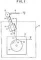
- FIG. 1 A device suitable for the implementation of this invention is illustrated in FIG. 1.
- a tube 10 is employed for containing a molten semiconductor material 12.
- the semiconductor material 12 is maintained molten by a furnace 14 which surrounds the tube 10.
- the tube 10 has a nozzle 16 which is employed to direct a molten stream 18 of the semiconductor material 12. Examples of such semiconductor materials are Si, Ge, and Ga-As.
- a gas supply tube 20 feeds gas into the tube 10 via a regulating valve 22.
- the regulating valve 22 controls pressure in the tube 10 above the molten semiconductor material 12. This pressure serves to discharge the molten semiconductor material 12 through the nozzle 16 and forms the stream 18.
- the stream 18 impinges on a rotating wheel 24.
- the stream 18 impacts the wheel 24 at an angle 6 such that there is a component of the stream direction which is in the direction of a tangent to the rotating wheel 24 at the point of contact 25. This component should be in the direction of the rotation.
- the wheel 24 is driven from a power drive 26 such as a motor.
- the wheel 24 should be a conducting material. Stainless steel, as well as copper, have been found to be satisfactory materials.
- the stream 18 impinges on the rotating cylindrical surface 28 thereby generating a semiconductor ribbon 30.
- a gas is supplied to the gas supply tube 20 and pressure.? in the tube 10 is maintained above the semiconductor material by the regulating valve 22. This pressure p controls the discharge of the stream 18 from the nozzle 16. The stream 18 impinges upon the wheel 24 which is rotating as illustrated with an angular speed ⁇ .
- the cylindrical surface 28 may not obtain velocities greater than 36 m/s without substantially reducing the ultimate average grain size of the resulting semiconductor ribbon 30.
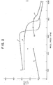
- FIG.. 2 offers a graphical representation of the effect of wheel speed on the average grain size.
- semiconductor material ribbons were generated on a copper wheel, having a diameter of 7,6 cm.
- Curves A, B and C are for silicon where the molten silicon is heated to about 1500 C and the gas injection pressure p was maintained at respectively 4 psig, 8 psig, and 15 psig for a nozzle having a nominal opening 1 mm in diameter. As the pressure is increased the ribbon becomes thinner and above about 15 psig the ribbon becomes discontinuous and forms flakes. It is apparent that as one increases the pressure there is an increase in the ultimate grain size which can be obtained.
- Wheel speed has a marked effect on the ultimate grain size. It can be seen that at rpm (revolutions per minute) values of about 9000, i.e. a surface speed of about 36 m/s, the grain size has dropped to the neighborhood of slightly less than 10 ⁇ m and as the velocity of the wheel is further increased the change in grain size is not substantially affected. This decrease in grain size occurs for all pressures studied. The drop is sharpest for curves B and C.
- the velocity of the wheel is presented both in terms of rotational speed (rpm) and the linear velocity (m/s) of the cylindrical surface 28.
- the pressures are given in terms of the gas ejection pressure for the resulting semiconductor stream 18. It was found that changing the orifice diameter from 0,5 mm to 1,5 mm did not noticeably affect the grain size of the resulting ribbons.
- the linear velocity of the surface of the wheel as well as ejection pressure are the appropriate parameters for the control of relative grain size of the resulting ribbon. These parameters can be maintained independent of the geometry of the equipment employed.
- Curve D of FIG. 2 illustrates the effect of velocity on the grain size of germanium semiconductor ribbons. These ribbons were generated from molten germanium which was heated to about 1000 0 C and ejected at a pressure of 15 psig through a nozzle having a nominal diameter of 1 mm. As can be seen by comparing curves C and D, the germanium data as is the case for the silicon data show little dependence of size or speed at low speeds. The tabular data used to generate curve D has been incorporated into Table I.
- Both germanium and silicon form oxides on the surface of the resulting ribbons when the ribbons are generated in an atmosphere of air. These oxides are sufficient to provide an intermediate layer between the silicon and a metal deposited thereon. The resulting metal silicon junctions form Schottky barriers.
- the oxide may be prevented by generating the ribbon under a protective atmosphere.
- Argon and helium have been found to be effective atmospheres in which to generate the ribbons.
- the wheel 24 and nozzle 16 should be placed in a chamber 32 as illustrated by the broken line in FIG. 1. This chamber will allow the atmosphere to be controlled.
- the present invention will be of use in the semiconductor industry and in particular in solar cell production.
Landscapes
- Engineering & Computer Science (AREA)
- Mechanical Engineering (AREA)
- Liquid Deposition Of Substances Of Which Semiconductor Devices Are Composed (AREA)
- Photovoltaic Devices (AREA)
Applications Claiming Priority (2)
| Application Number | Priority Date | Filing Date | Title |
|---|---|---|---|
| US15025780A | 1980-05-15 | 1980-05-15 | |
| US150257 | 1980-05-15 |
Publications (2)
| Publication Number | Publication Date |
|---|---|
| EP0040306A1 true EP0040306A1 (de) | 1981-11-25 |
| EP0040306B1 EP0040306B1 (de) | 1984-07-25 |
Family
ID=22533727
Family Applications (1)
| Application Number | Title | Priority Date | Filing Date |
|---|---|---|---|
| EP81102203A Expired EP0040306B1 (de) | 1980-05-15 | 1981-03-24 | Verfahren zur Herstellung grobkörniger Halbleiterbänder |
Country Status (3)
| Country | Link |
|---|---|
| EP (1) | EP0040306B1 (de) |
| JP (1) | JPS577119A (de) |
| DE (1) | DE3164971D1 (de) |
Cited By (1)
| Publication number | Priority date | Publication date | Assignee | Title |
|---|---|---|---|---|
| WO1987000460A1 (fr) * | 1985-07-21 | 1987-01-29 | Concast Standard Ag | Procede et dispositif de coulee de bandes metalliques directement a partir de la masse en fusion |
Families Citing this family (1)
| Publication number | Priority date | Publication date | Assignee | Title |
|---|---|---|---|---|
| JP6654751B2 (ja) | 2016-09-14 | 2020-02-26 | トヨタ自動車株式会社 | 車両用変速機 |
Citations (3)
| Publication number | Priority date | Publication date | Assignee | Title |
|---|---|---|---|---|
| US3812901A (en) * | 1973-01-30 | 1974-05-28 | Battelle Development Corp | Method of producing continuous filaments using a rotating heat-extracting member |
| US4177856A (en) * | 1978-08-28 | 1979-12-11 | General Electric Company | Critical gas boundary layer Reynolds number for enhanced processing of wide glassy alloy ribbons |
| DE2830522A1 (de) * | 1978-07-12 | 1980-01-31 | Licentia Gmbh | Verfahren und vorrichtung zur herstellung von folien, baendern oder platten aus silizium |
Family Cites Families (4)
| Publication number | Priority date | Publication date | Assignee | Title |
|---|---|---|---|---|
| US3297436A (en) * | 1965-06-03 | 1967-01-10 | California Inst Res Found | Method for making a novel solid metal alloy and products produced thereby |
| US4142571A (en) * | 1976-10-22 | 1979-03-06 | Allied Chemical Corporation | Continuous casting method for metallic strips |
| JPS5472954A (en) * | 1977-11-23 | 1979-06-11 | Noboru Tsuya | Semiconductor thin film and method of fabricating same |
| JPS5552218A (en) * | 1978-10-12 | 1980-04-16 | Noboru Tsuya | Semiconductor thin belt and manufacturing method thereof |
-
1981
- 1981-03-24 EP EP81102203A patent/EP0040306B1/de not_active Expired
- 1981-03-24 DE DE8181102203T patent/DE3164971D1/de not_active Expired
- 1981-04-06 JP JP5067881A patent/JPS577119A/ja active Pending
Patent Citations (3)
| Publication number | Priority date | Publication date | Assignee | Title |
|---|---|---|---|---|
| US3812901A (en) * | 1973-01-30 | 1974-05-28 | Battelle Development Corp | Method of producing continuous filaments using a rotating heat-extracting member |
| DE2830522A1 (de) * | 1978-07-12 | 1980-01-31 | Licentia Gmbh | Verfahren und vorrichtung zur herstellung von folien, baendern oder platten aus silizium |
| US4177856A (en) * | 1978-08-28 | 1979-12-11 | General Electric Company | Critical gas boundary layer Reynolds number for enhanced processing of wide glassy alloy ribbons |
Cited By (1)
| Publication number | Priority date | Publication date | Assignee | Title |
|---|---|---|---|---|
| WO1987000460A1 (fr) * | 1985-07-21 | 1987-01-29 | Concast Standard Ag | Procede et dispositif de coulee de bandes metalliques directement a partir de la masse en fusion |
Also Published As
| Publication number | Publication date |
|---|---|
| JPS577119A (en) | 1982-01-14 |
| DE3164971D1 (en) | 1984-08-30 |
| EP0040306B1 (de) | 1984-07-25 |
Similar Documents
| Publication | Publication Date | Title |
|---|---|---|
| US5959341A (en) | Thermoelectric semiconductor having a sintered semiconductor layer and fabrication process thereof | |
| US3881542A (en) | Method of continuous casting metal filament on interior groove of chill roll | |
| SE7812173L (sv) | Supraledande material samt slett for dess framstellning | |
| US4339255A (en) | Method and apparatus for making a modified amorphous glass material | |
| US3939900A (en) | Apparatus for continuous casting metal filament on interior of chill roll | |
| US4515650A (en) | Method for producing large grained semiconductor ribbons | |
| EP0040306B1 (de) | Verfahren zur Herstellung grobkörniger Halbleiterbänder | |
| EP0017723A1 (de) | Verfahren und Vorrichtung zum Herstellen metallischen Glaspulvers | |
| JP3604308B2 (ja) | ナノコンポジット磁石用原料合金、その粉末および製造方法、ならびにナノコンポジット磁石粉末および磁石の製造方法 | |
| EP0486056B1 (de) | Verfahren zur Herstellung einer synthetischen Diamantstruktur | |
| EP0040488A1 (de) | Verfahren zur Herstellung einer Bandstruktur | |
| US4363769A (en) | Method for manufacturing thin and flexible ribbon wafer of _semiconductor material and ribbon wafer | |
| US4332838A (en) | Particulate thin film fabrication process | |
| US4942057A (en) | Making an amorphous layer | |
| EP0721998A1 (de) | Verfahren und Vorrichtung zur Diamantabscheidung mittels CVD | |
| US4402905A (en) | Production of a polycrystalline silicon aluminum alloy by a hot pressing technique | |
| US4781754A (en) | Rapid solidification of plasma sprayed magnetic alloys | |
| US4293023A (en) | Method and device for the manufacture of metal bands | |
| US6329674B1 (en) | Composite structure with a growth substrate having a diamond layer and a plurality of microelectronic components, and process for producing such a composite structure | |
| US4551291A (en) | Surface improvement of semiconductors in high speed casting | |
| JPH0457609B2 (de) | ||
| JPH02145710A (ja) | 金属微粉末の製造方法 | |
| JP2008207984A (ja) | 結晶シリコン粒子の製造方法及び結晶シリコン粒子の製造装置 | |
| JPS63199809A (ja) | 粉末製造装置 | |
| SU1069932A1 (ru) | Способ получени быстрозакаленной металлической ленты |
Legal Events
| Date | Code | Title | Description |
|---|---|---|---|
| PUAI | Public reference made under article 153(3) epc to a published international application that has entered the european phase |
Free format text: ORIGINAL CODE: 0009012 |
|
| AK | Designated contracting states |
Designated state(s): DE FR GB IT |
|
| 17P | Request for examination filed |
Effective date: 19820427 |
|
| GRAA | (expected) grant |
Free format text: ORIGINAL CODE: 0009210 |
|
| AK | Designated contracting states |
Designated state(s): DE FR GB IT |
|
| PG25 | Lapsed in a contracting state [announced via postgrant information from national office to epo] |
Ref country code: IT Free format text: LAPSE BECAUSE OF FAILURE TO SUBMIT A TRANSLATION OF THE DESCRIPTION OR TO PAY THE FEE WITHIN THE PRESCRIBED TIME-LIMIT;WARNING: LAPSES OF ITALIAN PATENTS WITH EFFECTIVE DATE BEFORE 2007 MAY HAVE OCCURRED AT ANY TIME BEFORE 2007. THE CORRECT EFFECTIVE DATE MAY BE DIFFERENT FROM THE ONE RECORDED. Effective date: 19840725 |
|
| REF | Corresponds to: |
Ref document number: 3164971 Country of ref document: DE Date of ref document: 19840830 |
|
| ET | Fr: translation filed | ||
| PLBE | No opposition filed within time limit |
Free format text: ORIGINAL CODE: 0009261 |
|
| STAA | Information on the status of an ep patent application or granted ep patent |
Free format text: STATUS: NO OPPOSITION FILED WITHIN TIME LIMIT |
|
| 26N | No opposition filed | ||
| PGFP | Annual fee paid to national office [announced via postgrant information from national office to epo] |
Ref country code: DE Payment date: 19910323 Year of fee payment: 11 |
|
| PGFP | Annual fee paid to national office [announced via postgrant information from national office to epo] |
Ref country code: GB Payment date: 19920210 Year of fee payment: 12 |
|
| PG25 | Lapsed in a contracting state [announced via postgrant information from national office to epo] |
Ref country code: DE Effective date: 19921201 |
|
| PGFP | Annual fee paid to national office [announced via postgrant information from national office to epo] |
Ref country code: FR Payment date: 19930226 Year of fee payment: 13 |
|
| PG25 | Lapsed in a contracting state [announced via postgrant information from national office to epo] |
Ref country code: GB Effective date: 19930324 |
|
| GBPC | Gb: european patent ceased through non-payment of renewal fee |
Effective date: 19930324 |
|
| PG25 | Lapsed in a contracting state [announced via postgrant information from national office to epo] |
Ref country code: FR Effective date: 19941130 |
|
| REG | Reference to a national code |
Ref country code: FR Ref legal event code: ST |