EP0040752A2 - Connecteurs galvaniquement découplables pour énergie et/ou signaux électriques - Google Patents
Connecteurs galvaniquement découplables pour énergie et/ou signaux électriques Download PDFInfo
- Publication number
- EP0040752A2 EP0040752A2 EP81103651A EP81103651A EP0040752A2 EP 0040752 A2 EP0040752 A2 EP 0040752A2 EP 81103651 A EP81103651 A EP 81103651A EP 81103651 A EP81103651 A EP 81103651A EP 0040752 A2 EP0040752 A2 EP 0040752A2
- Authority
- EP
- European Patent Office
- Prior art keywords
- coupling
- housing
- insert
- energy
- coupling point
- Prior art date
- Legal status (The legal status is an assumption and is not a legal conclusion. Google has not performed a legal analysis and makes no representation as to the accuracy of the status listed.)
- Granted
Links
- 230000008054 signal transmission Effects 0.000 title claims abstract description 24
- 230000008878 coupling Effects 0.000 claims abstract description 81
- 238000010168 coupling process Methods 0.000 claims abstract description 81
- 238000005859 coupling reaction Methods 0.000 claims abstract description 81
- 238000007667 floating Methods 0.000 claims abstract description 15
- 238000007373 indentation Methods 0.000 claims abstract description 12
- 230000013011 mating Effects 0.000 claims abstract description 3
- 210000002445 nipple Anatomy 0.000 claims description 7
- 239000000463 material Substances 0.000 claims description 5
- 239000011810 insulating material Substances 0.000 claims description 2
- 238000005192 partition Methods 0.000 claims description 2
- 238000012546 transfer Methods 0.000 claims description 2
- 238000012432 intermediate storage Methods 0.000 claims 1
- 238000009413 insulation Methods 0.000 abstract description 4
- 230000005540 biological transmission Effects 0.000 description 12
- 229910052751 metal Inorganic materials 0.000 description 8
- 239000002184 metal Substances 0.000 description 8
- 239000004033 plastic Substances 0.000 description 8
- 239000010408 film Substances 0.000 description 7
- 230000007246 mechanism Effects 0.000 description 6
- 239000000725 suspension Substances 0.000 description 6
- 238000000926 separation method Methods 0.000 description 4
- 238000012545 processing Methods 0.000 description 3
- 210000000078 claw Anatomy 0.000 description 2
- 238000010276 construction Methods 0.000 description 2
- 238000005516 engineering process Methods 0.000 description 2
- 238000003780 insertion Methods 0.000 description 2
- 230000037431 insertion Effects 0.000 description 2
- 239000004952 Polyamide Substances 0.000 description 1
- 229910000831 Steel Inorganic materials 0.000 description 1
- 230000009471 action Effects 0.000 description 1
- 229910052782 aluminium Inorganic materials 0.000 description 1
- XAGFODPZIPBFFR-UHFFFAOYSA-N aluminium Chemical compound [Al] XAGFODPZIPBFFR-UHFFFAOYSA-N 0.000 description 1
- 238000009530 blood pressure measurement Methods 0.000 description 1
- 230000003749 cleanliness Effects 0.000 description 1
- 239000004020 conductor Substances 0.000 description 1
- 239000013039 cover film Substances 0.000 description 1
- 238000013461 design Methods 0.000 description 1
- 230000003670 easy-to-clean Effects 0.000 description 1
- 239000003365 glass fiber Substances 0.000 description 1
- 239000012774 insulation material Substances 0.000 description 1
- 230000009191 jumping Effects 0.000 description 1
- 238000004519 manufacturing process Methods 0.000 description 1
- 238000005259 measurement Methods 0.000 description 1
- 238000012986 modification Methods 0.000 description 1
- 230000004048 modification Effects 0.000 description 1
- 239000013307 optical fiber Substances 0.000 description 1
- 229920002647 polyamide Polymers 0.000 description 1
- 239000013535 sea water Substances 0.000 description 1
- 238000007789 sealing Methods 0.000 description 1
- 239000010959 steel Substances 0.000 description 1
- 238000002604 ultrasonography Methods 0.000 description 1
Images


Classifications
-
- H—ELECTRICITY
- H05—ELECTRIC TECHNIQUES NOT OTHERWISE PROVIDED FOR
- H05K—PRINTED CIRCUITS; CASINGS OR CONSTRUCTIONAL DETAILS OF ELECTRIC APPARATUS; MANUFACTURE OF ASSEMBLAGES OF ELECTRICAL COMPONENTS
- H05K9/00—Screening of apparatus or components against electric or magnetic fields
- H05K9/0062—Structures of standardised dimensions, e.g. 19" rack, chassis for servers or telecommunications
-
- H—ELECTRICITY
- H05—ELECTRIC TECHNIQUES NOT OTHERWISE PROVIDED FOR
- H05K—PRINTED CIRCUITS; CASINGS OR CONSTRUCTIONAL DETAILS OF ELECTRIC APPARATUS; MANUFACTURE OF ASSEMBLAGES OF ELECTRICAL COMPONENTS
- H05K7/00—Constructional details common to different types of electric apparatus
- H05K7/14—Mounting supporting structure in casing or on frame or rack
- H05K7/1422—Printed circuit boards receptacles, e.g. stacked structures, electronic circuit modules or box like frames
- H05K7/1427—Housings
-
- H—ELECTRICITY
- H05—ELECTRIC TECHNIQUES NOT OTHERWISE PROVIDED FOR
- H05K—PRINTED CIRCUITS; CASINGS OR CONSTRUCTIONAL DETAILS OF ELECTRIC APPARATUS; MANUFACTURE OF ASSEMBLAGES OF ELECTRICAL COMPONENTS
- H05K7/00—Constructional details common to different types of electric apparatus
- H05K7/18—Construction of rack or frame
Definitions
- the invention relates to a galvanically isolating coupling point for energy and / or signal transmission, with primary and secondary coupling elements, one of which is arranged in an indentation of a first housing and the other sits in a second housing, which is a plug-in part in the indentation of the first housing is insertable, the coupling members having mating coupling surfaces, via which the coupling point is produced by joining together when the plug connection is made.
- Coupling points of this type for example from DE-GM 77 36 156 (or DE-PS 27 52 783), are known from medical technology for devices for taking and processing physiological signals, such as in particular EKG, pressure, temperature etc.
- GB-PS 13 83 577 describes the use of such a coupling point on hulls in sea water, while GB-PS 13 66 134 and GB-PS 14 47 469 show examples of coupling points of general technology in which coils or for transmitting energy optical fibers can be used as primary and secondary coupling elements for the transmission of signals. With all of these coupling elements, there is now a desire for the highest possible coupling efficiency.
- the object of the present invention is to set up a coupling point of the type mentioned at the outset which, with a particularly high dielectric strength and with optimal insulation, allows energy and / or signal transmission with an optimally high degree of efficiency.
- the object is achieved in that the coupling elements with at least one coupling surface, but preferably with both mutually assigned coupling surfaces, are suspended in a floating and resilient manner in the respective housing.
- the floating and springy suspension of the coupling links enables particularly intensive contact in the transmission path at the point of separation of the transmission between the coupling links assigned to each other.
- This intensive coupling means that there is hardly any wastage; Despite optimal insulation at the separation point, the transmission is extremely effective.
- both the coupling elements for energy transmission and the coupling element can which are floating and suspended for signal transmission.
- the floating suspension will always be recommended where the coupling links have relatively large coupling surfaces.
- Relatively large coupling surfaces now always have coupling elements that are used for energy transmission.
- the primary and / or associated secondary transformer half part of an energy transformer should always be suspended in a floating and resilient manner.
- the signal coupling elements which generally have a much smaller coupling area and in which losses in signal transmission are not as important as losses in energy transmission, can also be permanently installed in the respective housing;
- the housings can be provided, for example, with niches or inserts or the like for receiving the light transmitters or assigned light receivers.
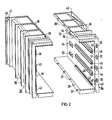
- FIG. 1 shows the device with a device housing 1 constructed in inches, with the side walls 2 and 3, the rear wall 4 and front surface 5, the base surface 6 and the cover surface 7, which is only indicated in broken lines.
- the device housing 1 is, for example, by two partition walls 8, 9 divided into three chambers 10, 11 and 12 inside.
- a cathode-ray tube (not shown) for displaying signals is located in the chamber 10.
- the chamber 11 takes conductors, for example plates with components for signal processing or signal display.
- the chamber 12, on the other hand, serves to receive the insulating body 13 according to the invention, which is designed as a box open at the front, inside of which a total of four device inserts 15, 16, 17 and 18 can be inserted from the front opening 14.
- the chamber 12 of the device housing can thus be defined, for example, as an indentation, which is lined with an insulating body 13, which in turn serves to accommodate inserts.
- the insulating body 13 itself can equally well be referred to as an indentation, which is used to hold plug-in units.
- the device bays are part of the signal transmission system. In terms of circuitry, they can be constructed internally as described in detail in DE-GM 77 36 156 (or DE-PS 27 52 783).
- each insert has a jacket made of insulation material with high dielectric strength, which in addition to the circuit boards with components and metal shielding for these components also carries the first half elements of a coupling point for energy and signal transmission, while the matching second half elements specifically sit in the rear surface of the insulating body 13 with connection to the free space of the chamber 12, as will be explained in more detail later.
- the device shown in FIG. 1 is specifically an electromedical device.
- the slots 15 to 18 are therefore part of the signal transmission system for physiological signals which are removed from the body of a patient by means of suitable pickups.
- consumers (not shown) are positioned on the patient's body and coupled to the respective insert 15 to 18 via a signal cable (also not shown).
- Inserts 15 to 18 have sockets 19 to 22 for the corresponding plugs of the signal cables for this purpose.
- the use of inserts is also possible, in which the customers are always permanently connected to the respective insert via signal cables (i.e. not in a plug connection). The latter case is appropriate if the individual slide-in housing is of relatively small volume.
- the slot with the permanently connected cable is then to be understood as a device plug.
- the front plate 5 is specially designed as a film plate. All operating and / or display elements are therefore in the plane of the film, as indicated by the symbols 23, 24. The same also applies to the picture window 25 for the screen of the cathode-ray tubes to be mounted or also for the front surfaces of the inserted plug-in units 15 to 18.
- the front surfaces of the plug-in units are also together with the built-in operating and display elements 25 to 29 (also shown only schematically). 28 and 29 are, for example, light emitting diodes) in the film level of the front plate 5.
- the arrangement in one level prohibits the attachment of handles to the inserts, with the aid of which inserted inserts can be pulled out of the bulge of the device housing.
- each insert is therefore specially equipped with an ejection mechanism on the rear wall of the insulating body 13, which comes into action when a locking device which locks the insert in the cavity after insertion by manual actuation of a release button arranged on the device housing is released.
- the individual release buttons for the plug-in units are shown in FIG. 1 on the rightmost edge of the front panel 5 with the reference numbers 30 to 33 indicated. Further details regarding the structure and functioning of the ejection mechanism in connection with the locking device are described below.
- 15 is, for example, a C0 2 insert, 16 an insert for pressure measurement, 17 an insert for EKG measurement and 18 a temperature insert.
- any other slide-in module for a different measured variable.
- the circumference of the insulating body 13 is composed of two half shells 34 and 35. Both half-shells are made of plastic.Amino-butadiene-styrene (ABS), which is easy to shape and is also relatively inexpensive.
- ABS plastic.Amino-butadiene-styrene
- the two half shells 34 and 35 are specially shaped as rib bodies.
- Each of the shells 34 and 35 thus includes ribs 36 on its circumference, which hold the inner wall of the insulating body, including insulating layers of air between the ribs, at a predeterminable distance from the metal walls of the housing chamber 12.
- the depth of the grooves in particular on the side walls of the half shells, is approximately 7 mm. On the upper and lower surfaces of the half-shells, the depth drops to a value of up to about 3 mm for assembly reasons.
- the thickness of the ribs is approximately 1.5 mm.
- the material width of the inner wall of the half-shells is approx. 3 mm.
- the insulating body composed of two half-shells 34 and 35 has an outer width of 2/8 ", measured from outer ribs to outer ribs.
- the height of the box-shaped insulating part is approximately 180 mm (corresponding to four height units HE).
- This dimensioning of the rib body 13 and the Selection of the corresponding iso Luring plastic lead in the present embodiment that the capacity between metal parts within the housing of the slots 15 to 18 and metal parts outside the insulating body 13 (shielding walls of the chamber 12 of the device housing or metal parts located on the rear wall of the insulating body 13), based on an operating voltage of 220 V and 50 Hz, is limited to a value ⁇ 130 pF. With this capacity, a possibly flowing working current is harmlessly low ( ⁇ 10 / uA).
- the two half-shells 34 and 35 of the insulating body on the mutually facing mounting edges comprise bolts 37 on each mounting edge of the one half-part, which fit into corresponding adjustment holes 38 on the opposite edge of the other half-part.
- the two half-shells 34 and 35 After the two half-shells 34 and 35 have been joined together, they are screwed to one another on the joining strips at the front via screw holes 39 on the cover side and corresponding screw holes 39 on the base side, each with a screw.
- the lower surfaces of the two half-shells are pressed together on the back by a special shape of the rear wall, which can be inserted into two grooves 41, 42 on the rear longitudinal edges of the assembled half-shells 34 and 35.
- the insulating body 13 composed of the two half-shells then forms a box which is open at the front and into which the inserts can be pushed.
- the two half-shells have longitudinal rails 43 to 46 on their inner wall for the tier-wise insertion of the individual inserts 15 to 18. These longitudinal rails are shaped in such a way that a relatively flat wall bulge 47 followed by a more bulging longitudinal web 48 (shown using the example of the rail 44).
- the release buttons for the locking lever system are again indicated at 30 to 33 on the right outer edge of the half shell 34.
- the keys 30 to 33 protrude only by such a distance from openings 49 to 52 of the edge of the half-shell 34 that after mounting the insulating body in the chamber 12 of the device housing 1 when the front surface 5 is covered with the film, the end face of each latch key approximately lies in the plane of the cover film of the front plate 5.
- a release button 30 to 33 is then actuated by pressing the film at the location of the release button. Pressing a release button, 30 to 33 causes a release lever to be actuated specifically in the present case via a lever system.
- FIG. 2 The locking lugs of the respective latch levers, which engage in a groove on a side edge of the insert in the inserted state of the insert, are shown in FIG. 2 on the rear inside of the right half-shell with 53 to 56 indicated. Further details on the structure and mode of operation of the locking device can be found in the following description of FIG. 4.
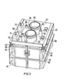
- FIG. 3 shows, in a partially broken view, the half-shells 34 and 35 joined together to form the whole body obliquely from below and rotated by approximately 180 ° in relation to the illustration in FIG. 2.
- the back plate 57 pushed into the grooves 41 and 42 is also shown.
- the groove webs 58 and 59 of this back plate slide at the lowest end shortly before the plate is fully inserted over two slightly slanted surfaces 60 and 61 on the rear lower edge of the lower surfaces of the two half-shells 34 and 35.
- the groove webs thus exert pressure on their lower edges via the increasing inclined surface 60 or 61 on the undersides of the two half-shells.
- the two half-shells are pressed together at this point and thus adhere well to one another.
- the back plate 57 is also made of plastic, preferably ABS again. It is not only the rear end part of the insulating body 13; rather, the back plate 57 also serves as a support for those sub-members of the coupling point which, as device-side half-parts, match the half-parts in the interior of the inserts. In FIG. 3, the back plate therefore has a total of four receiving cylinders for transmitter bodies for energy transmission, of which only two can be seen because of the partially broken illustration, which are denoted by 62 and 63. The upper edge of each assembly cylinder 62, 63 etc. facing away from the back plate 57 is thinned like a web.
- the shoulder 64 of the web thinning of the upper edge serves as a support for a mounting plate which is centered by the actual upper edge round web 65.
- the mounting plate is in turn the carrier of the transmitter body in floating suspension; she herself sits on a circuit board on which the for the energy transmission or signal transmission required electronic components are mounted.
- the signal is transmitted from the insert towards the signal processing parts of the device by means of luminescent diodes, preferably in the infrared range.
- four device-side light receivers for example photodiodes
- the mounting niches for the light receivers are indicated on the mounting plate 57 with the reference numbers 66, 67 etc.
- inserts 68, 69, etc. for transmitting diodes are also provided for signal transmission (switching or other control signals) from the interior of the device housing in the direction of inserts on the rear plate 57 of the insulating body.
- the luminescent diodes to be used there are then the primary coupling elements for a transmission case; the assigned receivers sit as secondary coupling links within the slide-in housing.
- the back plate 57 also includes screw feet 70 for screwing the circuit board carrying the mounting plate, and on the left side of the plate 57 the first two ejectors 71 and 72 of a total of four ejectors can be seen for one insert each.
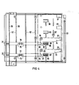
- FIG. 4 shows, as already indicated above, the right side wall of the Iso, seen from the opening lier emotionss 13 on which the lever system for locking the individual slots 15 to 18 is mounted.
- This lever system includes a latch lever 73, 74 etc. with the locking lugs 53 to 56 shown in FIG. 2 for each insert.
- Each latch lever 73, 74 etc. is assigned an actuating lever 75, 76 etc. which, when pressed on the end release button 30, 31, etc. is deflected and the latch lever is actuated.
- Each deflection lever 75, 76 etc. consists of two parts, each of which can be adjusted to a desired overall length of the lever by means of an adjusting screw 77, 78 etc.
- the locking lug jumps out of the corresponding locking groove of the insert and the insert is ejected from the insulating housing at the same time by the ejection mechanism.
- the longitudinal lever 75, 76 etc. in recesses 92 of the ribs of the side wall are turned.
- a plastic plate 93 (shown in broken lines) is used, which is screwed into a screw hole 93 'on the side wall of the insulating housing above the levers and springs.
- FIG. 5 shows the embodiment of an insert, for example insert 15 in FIG. 1.
- Each of the inserts comprises a casing 94 made of highly insulating plastic, e.g. ABS again.
- the highly insulating jacket 94 is provided along its longitudinal edges with the well-rounded slide channels 95 already mentioned and therefore also easy to clean.
- the latch groove 96 At the rear end of the upper right edge of the insert casing 94 there is the latch groove 96, into which a block 97 made of hard plastic, in particular polyamide glass fiber, is glued.
- the hard block 97 protects the latching groove 96 against excessive stress caused by the locking lever of the latch lever.
- the front opening of the casing 94 of each insert is sealed off with an insert front plate.
- FIG. 6 shows the rear surface 98 of the casing 94.
- This rear surface is thinned like a disk in the center (indicated by dashed lines) in the material.
- the thinning at this point ensures a particularly close coupling of the underlying transformer body on the side of the insert to that on the side of the device on the back plate of the insulating body in the end position of the insert.
- the window is red-injected plastic or a real infrared filter.
- the two windows are ultrasonically and ultrasonically insulated into the rear wall 98 by means of ultrasound.
- FIG. 7 shows in detail the ejection mechanism on the back plate 57 of the insulating body.
- a third ejection block 102 is also shown.
- a fourth ejection block is no longer included due to the broken representation drawn.
- Each block 71, 72, 102 etc. comprises a push member 103, 104, 105 etc.
- Each of these push members is connected to a push rod 106, 107, 108 etc., which is formed by a coil spring 109, 110, 111 etc. in the interior 112, 113, 114 etc. of the respective ejection blocks is spring-mounted.
- Retaining rings 115, 116, 117 etc. are used for the external securing of the plunger.
- each plunger also actuates a switch, in particular a microswitch, in the sense that the power supply to the primary transformer on the device side is interrupted when an insert is ejected.
- FIG. 8 shows, as an exemplary embodiment, the inner structure of an insert 15 to 18.
- This inner structure is characterized in that a total of two printed circuit boards 120 and 121 are held between the front part 118 of the insert and a rear part 119 in the manner of a plug-in connection. Are on these circuit boards the essential electronic components for energy and signal transmission are assembled.
- This partial structure consisting of the front and rear surfaces and printed circuit boards is finally covered in a sandwich manner by two metal shielding plates 122 and 123 (for example made of aluminum or steel plate). Both shield plates 122 and 123 are provided with claws 124 and 125 on the front edge.
- the rear part 119 is made of metallized plastic for the purpose of shielding.
- the rear part 119 is at the same time a carrier of half parts of coupling points for energy and signal transmission.
- it carries, in floating suspension, a shell core for receiving a coil former as a secondary part of a coupling point for energy transmission from the device to the insert.
- An insert for a transmitter diode 138 (luminescent diode) is arranged on the left side for signal transmission from the insert to the device and a niche for a light receiver 139 (photodiode) is arranged on the right side for signal transmission from the insert to the insert.
- a signal cable harness 140 is used for the line connection between the front plate 118 (film front plate with integrated switches) of the insert and circuit boards 120, 121, while a signal cable harness 141 is used to connect the circuit boards to one another is provided.
- a plug connection 142, 143 is used to establish a line connection for the energy transmission from the coil former located in the shell core 137 to the associated circuit part on the printed circuit boards.
- the plug 142 is located on the rear part 119; the plug 143 is arranged on the printed circuit board 120.
- FIG. 9 shows a detail of a coupling point for energy transmission, as it appears when an insert is brought into its end position in the insulating housing. Accordingly, the rear surface of the slide-in housing 94 with material thinning 99 is shown in the center at 98 in broken and sectioned representation. The material thinner 99 is also provided with a centering cross 144. With 145 the transmitter carrier is designated.
- This carrier carries the insert-side shell core 137, already shown in FIG. 8, for receiving the secondary-side coil former.
- the shell core 137 is slotted; through the slot 146, the connecting wires for the coil core are simultaneously passed.
- the transformer carrier including the shell core and coil body is suspended by means of a holding nipple 147 including a spring 148 on the rear part 119.
- a locking ring 149 secures the arrangement against falling out.
- a similar construction also offers the suspension of the transmitter on the side of the device. With 57, the back plate of the insulating housing 13 is shown again.
- the back plate 57 carries Assembly cylinder 62 with shoulder 64 and centering web 65 for thinning the web of the upper edge.
- the mounting plate 151 for a transmitter carrier 152 on the device side with a mounted shell core 153 with a slot 154 for the coil body on the device sits on the upper edge of the receiving cylinder 62 designed in this way.
- the transmitter structure is again suspended from the mounting plate 151 by means of a holding nipple 155 and spring 156 and a locking ring 157.
- the mounting plate 151 is supported by a printed circuit board 159, which carries the electronic components required for energy and signal transmission.
- a snap nipple 158 is used to fasten the mounting plate to the circuit board, which is simply snapped into the circuit board.
- a mounting pin 160 is used between the transmitter carrier and the mounting plate and a pin 161 between the mounting plate and the printed circuit board, while 162 is a very thin sealing film which is stretched over the inner surface of the back plate 57.
Landscapes
- Engineering & Computer Science (AREA)
- Microelectronics & Electronic Packaging (AREA)
- Casings For Electric Apparatus (AREA)
- Measuring And Recording Apparatus For Diagnosis (AREA)
- Connector Housings Or Holding Contact Members (AREA)
- Measurement And Recording Of Electrical Phenomena And Electrical Characteristics Of The Living Body (AREA)
- Connecting Device With Holders (AREA)
- Photo Coupler, Interrupter, Optical-To-Optical Conversion Devices (AREA)
- Details Of Connecting Devices For Male And Female Coupling (AREA)
Applications Claiming Priority (2)
| Application Number | Priority Date | Filing Date | Title |
|---|---|---|---|
| DE19803019646 DE3019646A1 (de) | 1980-05-22 | 1980-05-22 | Galvanisch trennende koppelstelle fuer energie- und/oder signaluebertragung |
| DE3019646 | 1980-05-22 |
Publications (3)
| Publication Number | Publication Date |
|---|---|
| EP0040752A2 true EP0040752A2 (fr) | 1981-12-02 |
| EP0040752A3 EP0040752A3 (en) | 1982-04-14 |
| EP0040752B1 EP0040752B1 (fr) | 1984-09-12 |
Family
ID=6103100
Family Applications (1)
| Application Number | Title | Priority Date | Filing Date |
|---|---|---|---|
| EP81103651A Expired EP0040752B1 (fr) | 1980-05-22 | 1981-05-12 | Connecteurs galvaniquement découplables pour énergie et/ou signaux électriques |
Country Status (6)
| Country | Link |
|---|---|
| US (1) | US4491981A (fr) |
| EP (1) | EP0040752B1 (fr) |
| JP (1) | JPS6018110B2 (fr) |
| DE (2) | DE3019646A1 (fr) |
| DK (1) | DK223381A (fr) |
| ES (1) | ES8300239A1 (fr) |
Cited By (3)
| Publication number | Priority date | Publication date | Assignee | Title |
|---|---|---|---|---|
| EP0040753A3 (en) * | 1980-05-22 | 1983-04-27 | Siemens Aktiengesellschaft | Insulated plug-in unit with high voltage-stability |
| EP0284882A3 (fr) * | 1987-03-31 | 1989-06-28 | Siemens Aktiengesellschaft | Rack pour armoires de télécommunications |
| CN105342598A (zh) * | 2015-09-30 | 2016-02-24 | 付臣 | 心内科常规电子检测仪 |
Families Citing this family (38)
| Publication number | Priority date | Publication date | Assignee | Title |
|---|---|---|---|---|
| CA1198803A (fr) * | 1984-01-23 | 1985-12-31 | Frederick T. Cogan | Enceinte pour cartes a circuit imprime |
| US4612670A (en) * | 1984-05-16 | 1986-09-16 | General Dynamics Corporation | Electro-optical connection between electronic modules |
| US4700272A (en) * | 1986-06-26 | 1987-10-13 | Digital Equipment Corporation | Apparatus and method for compensation of thermal expansion of cooling fluid in enclosed electronic packages |
| US4725244A (en) * | 1987-07-02 | 1988-02-16 | Tektronix, Inc. | System for assembling an electronic work station |
| DE3813888A1 (de) * | 1988-04-20 | 1989-11-02 | Schleicher Elektronic Gmbh & C | Modul fuer eine aus mehreren auf einem traeger nebeneinander angeordneten modulen bestehenden steuerung |
| DE3819295A1 (de) * | 1988-06-07 | 1989-12-14 | Licentia Gmbh | Baugruppentraeger mit in fuehrungshalter einsetzbaren baugruppen |
| CA2062608A1 (fr) * | 1991-04-18 | 1992-10-19 | Steven W. Tanamachi | Capteur en deux parties assurant le couplage de signaux optique et le couplage de puissance du transformateur |
| US5090048A (en) * | 1991-05-22 | 1992-02-18 | General Electric Company | Shielded enclosure with an isolation transformer |
| EP0682322B1 (fr) * | 1991-09-09 | 2001-09-26 | Itt Manufacturing Enterprises, Inc. | Carte à puce |
| DE69202948T2 (de) * | 1991-09-11 | 1996-02-01 | Intel Corp., Santa Clara, Calif. | Speicherkarten-Erdungseinrichtung. |
| US5227954A (en) * | 1991-10-18 | 1993-07-13 | Epson Portland, Inc. | Arrangement for mounting disk drive in drive dock |
| US5207586A (en) * | 1991-10-24 | 1993-05-04 | Intel Corporation | Integral connector system for credit card size I/O card external connector |
| US5247427A (en) * | 1992-08-26 | 1993-09-21 | Data General Corporation | Disk array subsystem having elongated T-shaped guides for use in a data processing system |
| US5606704A (en) * | 1994-10-26 | 1997-02-25 | Intel Corporation | Active power down for PC card I/O applications |
| US6213651B1 (en) | 1999-05-26 | 2001-04-10 | E20 Communications, Inc. | Method and apparatus for vertical board construction of fiber optic transmitters, receivers and transceivers |
| US6901221B1 (en) | 1999-05-27 | 2005-05-31 | Jds Uniphase Corporation | Method and apparatus for improved optical elements for vertical PCB fiber optic modules |
| US20010030789A1 (en) * | 1999-05-27 | 2001-10-18 | Wenbin Jiang | Method and apparatus for fiber optic modules |
| US7116912B2 (en) * | 1999-05-27 | 2006-10-03 | Jds Uniphase Corporation | Method and apparatus for pluggable fiber optic modules |
| US6926551B1 (en) * | 2000-01-11 | 2005-08-09 | Infineon Technologies Ag | Pluggable transceiver latching mechanism |
| CN1200641C (zh) * | 2000-11-20 | 2005-05-11 | 美国西门子医疗解决公司 | 一种使用电隔离的组合功率和信号耦合器系统的便携病人监视器装置以及对接座 |
| US6942395B1 (en) | 2001-01-29 | 2005-09-13 | Jds Uniphase Corporation | Method and apparatus of pull-lever release for fiber optic modules |
| US6846115B1 (en) | 2001-01-29 | 2005-01-25 | Jds Uniphase Corporation | Methods, apparatus, and systems of fiber optic modules, elastomeric connections, and retention mechanisms therefor |
| US6659655B2 (en) * | 2001-02-12 | 2003-12-09 | E20 Communications, Inc. | Fiber-optic modules with housing/shielding |
| US6607308B2 (en) * | 2001-02-12 | 2003-08-19 | E20 Communications, Inc. | Fiber-optic modules with shielded housing/covers having mixed finger types |
| US6851867B2 (en) * | 2001-04-14 | 2005-02-08 | Jds Uniphase Corporation | Cam-follower release mechanism for fiber optic modules with side delatching mechanisms |
| US6840680B1 (en) | 2001-04-14 | 2005-01-11 | Jds Uniphase Corporation | Retention and release mechanisms for fiber optic modules |
| US6796715B2 (en) | 2001-04-14 | 2004-09-28 | E20 Communications, Inc. | Fiber optic modules with pull-action de-latching mechanisms |
| US6692159B2 (en) | 2001-04-14 | 2004-02-17 | E20 Communications, Inc. | De-latching mechanisms for fiber optic modules |
| US6994478B1 (en) | 2001-04-14 | 2006-02-07 | Jds Uniphase Corporation | Modules having rotatable release and removal lever |
| US6863448B2 (en) * | 2001-04-14 | 2005-03-08 | Jds Uniphase Corporation | Method and apparatus for push button release fiber optic modules |
| US7118281B2 (en) * | 2002-08-09 | 2006-10-10 | Jds Uniphase Corporation | Retention and release mechanisms for fiber optic modules |
| DE102005031268B3 (de) | 2005-07-05 | 2007-01-18 | Moeller Gmbh | Elektrische Schalteinrichtung |
| US20110168585A1 (en) * | 2010-01-12 | 2011-07-14 | Brigitte Helm-Bürgerhoff | Container Assembly for Storing Peripheral Computer Memory Devices |
| KR101460898B1 (ko) * | 2013-06-11 | 2014-11-14 | 현대오트론 주식회사 | 경사 구조물을 이용한 차량의 전자 제어 장치 및 그 제조 방법 |
| CN111935944B (zh) * | 2020-08-03 | 2021-06-08 | 马鞍山鑫霖电子科技有限公司 | 一种有源或无源通信设备综合集装架 |
| CN114077020A (zh) * | 2020-08-18 | 2022-02-22 | 华为技术有限公司 | 复合模块及其制造方法 |
| LU502656B1 (de) | 2022-08-11 | 2024-02-12 | Phoenix Contact Gmbh & Co | Gehäuse für eine elektrische Schaltung und zugehöriges Herstellungsverfahren |
| DE102022120280A1 (de) | 2022-08-11 | 2024-02-22 | Phoenix Contact Gmbh & Co. Kg | Gehäuse für eine elektrische Schaltung und zugehöriges Herstellungsverfahren |
Family Cites Families (13)
| Publication number | Priority date | Publication date | Assignee | Title |
|---|---|---|---|---|
| US2335205A (en) * | 1941-10-16 | 1943-11-23 | Philco Radio & Television Corp | Supporting means for radio coil units and the like |
| US2602842A (en) * | 1949-06-07 | 1952-07-08 | Motorola Inc | Railroad communication system |
| US2692972A (en) * | 1951-04-19 | 1954-10-26 | Albert K Edgerton | High-frequency moisture register with button-type electrode |
| DE1276684B (de) * | 1960-11-03 | 1968-09-05 | Licentia Gmbh | Loesbare elektrische Leitungskupplung zur UEbertragung von Wechselspannungen |
| FR2154364B1 (fr) * | 1971-10-01 | 1975-06-06 | Snecma | |
| GB1366134A (en) * | 1972-01-25 | 1974-09-11 | Victor Products Ltd | Electric circuit for supplying alternating current to a load |
| CA1034804A (fr) * | 1974-03-20 | 1978-07-18 | Northern Electric Company | Connecteurs de fibres optiques |
| US4012089A (en) * | 1974-04-08 | 1977-03-15 | The United States Of America As Represented By The Secretary Of The Navy | Electronic equipment enclosure |
| JPS5710405B2 (fr) * | 1974-06-05 | 1982-02-26 | ||
| GB1514909A (en) * | 1974-06-07 | 1978-06-21 | British Steel Corp | Electronic monitoring equipment |
| US4038625A (en) * | 1976-06-07 | 1977-07-26 | General Electric Company | Magnetic inductively-coupled connector |
| FR2376533A1 (fr) * | 1976-12-31 | 1978-07-28 | Socapex | Connecteur multivoies a detrompage automatique |
| DE2752783C2 (de) * | 1977-11-25 | 1979-08-30 | Siemens Ag, 1000 Berlin Und 8000 Muenchen | Gerät zum Erfassen und Verarbeiten von elektrischen Signalen |
-
1980
- 1980-05-22 DE DE19803019646 patent/DE3019646A1/de not_active Withdrawn
-
1981
- 1981-05-08 US US06/261,788 patent/US4491981A/en not_active Expired - Lifetime
- 1981-05-12 DE DE8181103651T patent/DE3165962D1/de not_active Expired
- 1981-05-12 EP EP81103651A patent/EP0040752B1/fr not_active Expired
- 1981-05-20 JP JP56076368A patent/JPS6018110B2/ja not_active Expired
- 1981-05-21 ES ES502385A patent/ES8300239A1/es not_active Expired
- 1981-05-21 DK DK223381A patent/DK223381A/da not_active Application Discontinuation
Cited By (3)
| Publication number | Priority date | Publication date | Assignee | Title |
|---|---|---|---|---|
| EP0040753A3 (en) * | 1980-05-22 | 1983-04-27 | Siemens Aktiengesellschaft | Insulated plug-in unit with high voltage-stability |
| EP0284882A3 (fr) * | 1987-03-31 | 1989-06-28 | Siemens Aktiengesellschaft | Rack pour armoires de télécommunications |
| CN105342598A (zh) * | 2015-09-30 | 2016-02-24 | 付臣 | 心内科常规电子检测仪 |
Also Published As
| Publication number | Publication date |
|---|---|
| ES502385A0 (es) | 1982-10-01 |
| JPS6018110B2 (ja) | 1985-05-08 |
| JPS5723484A (en) | 1982-02-06 |
| ES8300239A1 (es) | 1982-10-01 |
| EP0040752A3 (en) | 1982-04-14 |
| DE3165962D1 (en) | 1984-10-18 |
| EP0040752B1 (fr) | 1984-09-12 |
| DK223381A (da) | 1981-11-23 |
| DE3019646A1 (de) | 1981-11-26 |
| US4491981A (en) | 1985-01-01 |
Similar Documents
| Publication | Publication Date | Title |
|---|---|---|
| EP0040752B1 (fr) | Connecteurs galvaniquement découplables pour énergie et/ou signaux électriques | |
| EP0040754B1 (fr) | Dispositif de détection et de traitement de signaux électriques | |
| EP0040753B1 (fr) | Elément coulissant à isolation électrique élevée | |
| AT392386B (de) | Elektronisches geraet | |
| DE212017000146U1 (de) | Stromversorgungsschrank | |
| EP0504703A2 (fr) | Prothèse auditive avec des moyens électriques de contact disposés dans un compartiment pour pile | |
| DE19511508C2 (de) | Elektrischer Leiterplattenverbinder | |
| DE102018101871A1 (de) | Leuchtmodulanordnung | |
| EP0496972B1 (fr) | Connecteur à fiche spécialement pour connection détachable des conducteurs électriques | |
| DE19857624A1 (de) | Verbinderanordnung für flache Schaltungseinrichtungen | |
| DE60110994T2 (de) | Elektrisch-optisches Verbindungsmodul | |
| DE69307225T2 (de) | Mehrfacher Lichtschrankenfühler | |
| DE102006026910B4 (de) | Bedieneinheit für ein Hausgerät | |
| EP0263391B1 (fr) | Dispositif pour recevoir, préparer, exploiter et transmettre des signaux électriques | |
| DE3019596C2 (de) | Gerät zum Erfassen und Verarbeiten von elektrischen Signalen | |
| DE2719389B2 (de) | Gehäuse für Meßinstrumente | |
| EP4211503A1 (fr) | Module optoélectronique, connecteur de fiche optoélectronique et unité de sous-distribution optoélectronique | |
| EP0521329A1 (fr) | Appareil pour sourds adapté pour être supporté entièrement par l'oreille et méthode de production | |
| WO1989004559A1 (fr) | Boitier electronique pour service severe | |
| EP0918374A2 (fr) | Connecteur coaxial à haute fréquence | |
| DE60036130T2 (de) | Anzeigevorrichtung und rahmen für eine solche | |
| DE2829639C2 (de) | Elektrischer Baustein | |
| DE3132485A1 (de) | Isolierter einschub mit hoher spannungsfestigkeit | |
| DE2729649C3 (de) | Hochfrequenzdicht abgeschirmte Antennensteckdose mit einem Richtungskoppler | |
| DE102012010735A1 (de) | Elektrische Anschluss- und Verbindungsdose für ein Solarzellenmodul |
Legal Events
| Date | Code | Title | Description |
|---|---|---|---|
| PUAI | Public reference made under article 153(3) epc to a published international application that has entered the european phase |
Free format text: ORIGINAL CODE: 0009012 |
|
| AK | Designated contracting states |
Designated state(s): DE FR GB NL SE |
|
| 17P | Request for examination filed |
Effective date: 19811028 |
|
| PUAL | Search report despatched |
Free format text: ORIGINAL CODE: 0009013 |
|
| AK | Designated contracting states |
Designated state(s): DE FR GB NL SE |
|
| GRAA | (expected) grant |
Free format text: ORIGINAL CODE: 0009210 |
|
| AK | Designated contracting states |
Designated state(s): DE FR GB NL SE |
|
| REF | Corresponds to: |
Ref document number: 3165962 Country of ref document: DE Date of ref document: 19841018 |
|
| ET | Fr: translation filed | ||
| PLBE | No opposition filed within time limit |
Free format text: ORIGINAL CODE: 0009261 |
|
| STAA | Information on the status of an ep patent application or granted ep patent |
Free format text: STATUS: NO OPPOSITION FILED WITHIN TIME LIMIT |
|
| 26N | No opposition filed | ||
| GBPC | Gb: european patent ceased through non-payment of renewal fee | ||
| PG25 | Lapsed in a contracting state [announced via postgrant information from national office to epo] |
Ref country code: GB Effective date: 19881118 |
|
| PGFP | Annual fee paid to national office [announced via postgrant information from national office to epo] |
Ref country code: SE Payment date: 19940526 Year of fee payment: 14 |
|
| PGFP | Annual fee paid to national office [announced via postgrant information from national office to epo] |
Ref country code: NL Payment date: 19940531 Year of fee payment: 14 |
|
| EAL | Se: european patent in force in sweden |
Ref document number: 81103651.6 |
|
| PG25 | Lapsed in a contracting state [announced via postgrant information from national office to epo] |
Ref country code: SE Effective date: 19950513 |
|
| PG25 | Lapsed in a contracting state [announced via postgrant information from national office to epo] |
Ref country code: NL Effective date: 19951201 |
|
| NLV4 | Nl: lapsed or anulled due to non-payment of the annual fee |
Effective date: 19951201 |
|
| EUG | Se: european patent has lapsed |
Ref document number: 81103651.6 |
|
| PGFP | Annual fee paid to national office [announced via postgrant information from national office to epo] |
Ref country code: FR Payment date: 20000523 Year of fee payment: 20 |
|
| PGFP | Annual fee paid to national office [announced via postgrant information from national office to epo] |
Ref country code: DE Payment date: 20000717 Year of fee payment: 20 |