EP0042574A2 - Procédé pour la pulvérisation réactive et appareil de mise en oeuvre d'un tel procédé - Google Patents
Procédé pour la pulvérisation réactive et appareil de mise en oeuvre d'un tel procédé Download PDFInfo
- Publication number
- EP0042574A2 EP0042574A2 EP81104622A EP81104622A EP0042574A2 EP 0042574 A2 EP0042574 A2 EP 0042574A2 EP 81104622 A EP81104622 A EP 81104622A EP 81104622 A EP81104622 A EP 81104622A EP 0042574 A2 EP0042574 A2 EP 0042574A2
- Authority
- EP
- European Patent Office
- Prior art keywords
- gas
- film
- reactive
- target material
- reactive gas
- Prior art date
- Legal status (The legal status is an assumption and is not a legal conclusion. Google has not performed a legal analysis and makes no representation as to the accuracy of the status listed.)
- Granted
Links
Images


Classifications
-
- C—CHEMISTRY; METALLURGY
- C23—COATING METALLIC MATERIAL; COATING MATERIAL WITH METALLIC MATERIAL; CHEMICAL SURFACE TREATMENT; DIFFUSION TREATMENT OF METALLIC MATERIAL; COATING BY VACUUM EVAPORATION, BY SPUTTERING, BY ION IMPLANTATION OR BY CHEMICAL VAPOUR DEPOSITION, IN GENERAL; INHIBITING CORROSION OF METALLIC MATERIAL OR INCRUSTATION IN GENERAL
- C23C—COATING METALLIC MATERIAL; COATING MATERIAL WITH METALLIC MATERIAL; SURFACE TREATMENT OF METALLIC MATERIAL BY DIFFUSION INTO THE SURFACE, BY CHEMICAL CONVERSION OR SUBSTITUTION; COATING BY VACUUM EVAPORATION, BY SPUTTERING, BY ION IMPLANTATION OR BY CHEMICAL VAPOUR DEPOSITION, IN GENERAL
- C23C14/00—Coating by vacuum evaporation, by sputtering or by ion implantation of the coating forming material
- C23C14/0021—Reactive sputtering or evaporation
- C23C14/0036—Reactive sputtering
- C23C14/0047—Activation or excitation of reactive gases outside the coating chamber
Definitions
- This invention is related to an improvement of the known method of reactive sputtering.
- the reactive sputtering for growing a film on the semiconductor substrate is a method in which a synergetic effect of the chemical and physical vapour depositions is achieved.
- the temparature under which the film is deposited is relatively low in the reactive sputtering method, with the adhesive characteristic of the film being substantially enhanced.
- the method of reactive sputtering is effective to form an insulating film to cover the semiconductor devices or to insulate interconnecting layers already fabricated on a semiconductor substrate.
- the reactive sputtering method which uses a magnetron sputtering apparatus, crossed (at right angles) electric and magnetic fields are created near a target material to enhance the efficiency in generating plasma for activating the reactive gas. And thus, with a relatively low degree vacuum, atoms ejected by sputtering and a reactive gas are caused to react efficiently with each other. Because of this, the reactive sputtering method excells in forming a quality film having a high degree of adhesiveness, and has come to be frequently used.
- the invention as claimed is intended to remedy these drawbacks. It solves the technical problem described above and offers a method of fabrication of an insulating film which is chemically and electrically stable.
- reactive gas is activated in advance and then introduced into a reaction chamber, and the particles ejected from a target material in the reaction chamber and said reactive gas are caused to react to form a desired film on the surface of a substrate to be treated at a high rate of growth.
- a reaction chamber 1 made of glass or stainless steel which may be for example an apparatus called Type CFS-8EP, a product of Tokuda Co., Lts. of Kanagawa, Japan by a known vacuum pump system .2 comprising a rotary pump and cryo pump, not shown, which is capable of attaining a degree of vacuum in order of 5 x 10 -7 Torr.
- the chamber 1 is a cylindrical structure having a diameter and a height of approximately 50 cm and 60 am, respectively.
- a cathode 6 on which is placed a target material 7 having a diameter of 12.7 cm (5 inch).
- the cathode 6 is enclosed within an insulator 8 of silica or ceramic having anodes 9 attached to its upper end portions. These anodes 9 are grounded as shown.
- magnets are in turn enclosed within a tank 10 to which cooling water W is supplied in the direction as shown by an arrow.
- the cathode 6 is connected, via a matching box 12, to an RF (13.56 MHz) power source 11.
- RF 13.56 MHz
- SiN silicon nitride
- said 13.56 MHz power is applied from the source 11 via a matching box 12, and inert gas such as argon (Ar) gas and reactive gas, that is nitrogen (N 2 ) gas, are introduced into the reactive chamber 1 through inlets 13 and 14 equipped with a flow meter and a valve, respectively.
- a target material 7, for ecample silicon is selected for the purpose of growing or forming said film, and by impact of activated argon ions (Ar + ) on the target material 7, silicon particles are ejected therefrom to be caused to react with nitrogen redicals (N 2 * ).
- a film of SiN is thus formed on the surface of the seniconductor,substrate 4.
- FIG. 2 An apparatus which has been developed to carry out a method for overcoming the above-described deficiency of the prior art is shown in a schematic cross-sectional view of. Fig. 2.
- nitrogen (N 2 ) gas which is supplied from the inlet 14 is activated in a plasma generator 15 comprising a silica chamber 16 enclosed by shield plates 17.
- Microwaves of 2.45 GHz, power 1 KW generated by a microwave oscillator 18 are led through a waveguide 19 arranged to cross the silica chamber 16, and cause nitrogen gas which is introduced into the silica chamber 16, gas pressure in order of 10-1 Torr, to be turned into plasma.
- Nitrogen radicals (N 2 *) which have been created into plasma remain in their activated state even when introduced into the chamber 1 after having passed through a pipe of teflon, for example, of several meters length via another valve 20.
- Ar + argon ions
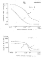
- Figures 3 and 4 show the composition and growth rates respectively of SiN film formed as described above, with the total gas pressure of activated nitrogen gas and untreated argon gas both introduces in the chamber being kept at 5 x 10⁻³ Torr, the RF power in the reaction chamber 1 is 800 W.-
- curves I represent data where nitrogen (N 2 ) gas is introduced into the reaction chamber 1 without previous treatment as was done in the conventional reactive sputtering method
- curves II represent data obtained ty the method of the present invention.
- the graphs of Fig. 3 illustrate the relationship between the partial pressure of nitrogen (N 2 ) gas and the composition of SiN film obtained by an X-ray photoelectron spectroscopy or electron spectroscopy for chemical analysis (ESCA).
- N 2 partial pressure of nitrogen
- ESA electron spectroscopy for chemical analysis
- Fig. 4 shows the relationship between the partial pressure of nitrogen (N 2 ) gas and the growth rate of the film of SiN formed by the conventional method and the method of the present invention respectively with the total gas pressure (the pressure of N 2 gas + Ar gas) being kept constant.
- the data show clearly that the growth rate under the present invention is higher than that under the conventional method.
- test results show that according to the method of the present invention, a good insulating film of SiN which is stoichiometrically very close to Si 3 N 4 may be grown at a rate of 1000 A per minute.
- Figures 5A, 5B and 5C show applications of the film formed by the method of the invention.
- a film 22 of Si 3 N 4 is grown approximately 1000 ⁇ thick directly or through a very thin film of silicon dioxide (Si0 2 ) on a silicon substrate 21 in accordance with the method of the inventions.
- a thick insulating layer 23 of SiO 2 is fabricated by a subsequent heat treatment using the film 22 of Si 3 N 4 as a mask. This is the well known process called a selective field oxidation.
- a film 32 of SiO 2 is formed on a silicon substrate 31.
- a first wiring or interconnecting layer 33 of aluminum is fabricated on the SiO 2 film 32.
- a film 35 of Si 3 N 4 is then grown according to the method of the invention to form an insulating layer between the first aluminum wiring layer 33 and a second wiring layer 34 of aluminum to be subsequently fabricated.
- This is an example of inter-layer insulation of multilayer wirings wherein the film 35 of Si 3 N 4 replaces that of phosphosilicate glass in the prior art.
- Fig. 5C shows a silicon gate MOS field effect transistor with inter-layer insulation.
- a source region S and a drain region D each 'of which is isolated by field insulating regions 42.
- a Gate G of polycrystal fine silicon is fabricated on an insulating film 43 of SiO 2 .
- An insulating layer 44 of Si3N4 is grown using the method of the invention.
- An interconnecting wiring layer 45 is then fabricated, as shown, on which a cover film 46 of Si 3 N 4 is grown approximately 1 ⁇ m thick, again by the method of the invention.
- Conditions of forming this film 4 ' 6 which is 1 ⁇ m thick are: pressure of argon (Ar) gas 4 x 10 -3 Torr, that of nitrogen (N 2 ) gas 1x 10 -3 Torr, powera 800 W, frequency 13.56 MHz. It took 'ten (10) minutes to grow this film which shows that a growth rate of 1000 A/minute.
- the frequency of the microwaves utilized is 2.45 GHz, the power is 1 KW, and the pressure within the chamber 16 of Fig. 2 is 10 1 Torr.
- nitrogen (N 2 ) gas was selected as reactive gas in forming or growing a film of SiN.
- gases such as oxygen (0 2 ) gas, nitric monoxide (NO) gas, nitrous oxide (N 2 0) gas or mixed gas of some of these may be used as reactive gas.
- a target material may be selected from a group of aluminum (Al), titanium (Ti), tantalum (ta) and so forth.
- the method of the invention is not confined to the formation of SiN film, but may also be applied to the formation of compounds such -as oxides or nitrides to which the reactive sputtering method can be applied
- the product obtained by the method of the invention is not limited to the insulating film.
- the method of reactive sputtering may be carried out to form stable reactive compound at a high growth rate according to the present invention.
- the invention serves the purpose of upgrading the quality of components in semiconductor devices in addition to improving efficiency of the manufacturing operations.
Landscapes
- Chemical & Material Sciences (AREA)
- Chemical Kinetics & Catalysis (AREA)
- Engineering & Computer Science (AREA)
- Materials Engineering (AREA)
- Mechanical Engineering (AREA)
- Metallurgy (AREA)
- Organic Chemistry (AREA)
- Physical Vapour Deposition (AREA)
Applications Claiming Priority (2)
| Application Number | Priority Date | Filing Date | Title |
|---|---|---|---|
| JP55085325A JPS5940227B2 (ja) | 1980-06-24 | 1980-06-24 | リアクティブスパッタリング方法 |
| JP85325/80 | 1980-06-24 |
Publications (3)
| Publication Number | Publication Date |
|---|---|
| EP0042574A2 true EP0042574A2 (fr) | 1981-12-30 |
| EP0042574A3 EP0042574A3 (en) | 1982-09-08 |
| EP0042574B1 EP0042574B1 (fr) | 1986-02-05 |
Family
ID=13855467
Family Applications (1)
| Application Number | Title | Priority Date | Filing Date |
|---|---|---|---|
| EP81104622A Expired EP0042574B1 (fr) | 1980-06-24 | 1981-06-16 | Procédé pour la pulvérisation réactive et appareil de mise en oeuvre d'un tel procédé |
Country Status (4)
| Country | Link |
|---|---|
| US (1) | US4384933A (fr) |
| EP (1) | EP0042574B1 (fr) |
| JP (1) | JPS5940227B2 (fr) |
| DE (1) | DE3173706D1 (fr) |
Cited By (4)
| Publication number | Priority date | Publication date | Assignee | Title |
|---|---|---|---|---|
| DE3611492A1 (de) * | 1986-04-05 | 1987-10-22 | Leybold Heraeus Gmbh & Co Kg | Verfahren und vorrichtung zum beschichten von werkzeugen fuer die zerspanungs- und umformtechnik mit hartstoffschichten |
| EP0303161A3 (en) * | 1987-08-11 | 1990-08-22 | Hartec Gesellschaft Fur Hartstoffe Und Dunnschichttechnik Mbh & Co. Kg | Method for coating objects by means of vacuum sputtering supported by magnetic fields |
| EP0837155A1 (fr) * | 1996-10-15 | 1998-04-22 | Applied Materials, Inc. | La fabrication des couches minces de TiN avec la génération eloignée de particules activées |
| EP0940481A1 (fr) * | 1998-03-05 | 1999-09-08 | Shincron Co., Ltd. | Procédé et appareillage pour la production d'une couche mince d'un composé métallique |
Families Citing this family (23)
| Publication number | Priority date | Publication date | Assignee | Title |
|---|---|---|---|---|
| EP0054201B1 (fr) * | 1980-12-11 | 1986-11-05 | Kabushiki Kaisha Toshiba | Appareil pour le décapage à sec et procédé |
| JPS59182207A (ja) * | 1983-03-31 | 1984-10-17 | Fujitsu Ltd | 高融点金属窒化膜の形成方法 |
| US4515668A (en) * | 1984-04-25 | 1985-05-07 | Honeywell Inc. | Method of forming a dielectric layer comprising a gettering material |
| EP0173164B1 (fr) * | 1984-08-31 | 1988-11-09 | Hitachi, Ltd. | Vaporisation à l'aide de micro-ondes |
| US4581100A (en) * | 1984-10-29 | 1986-04-08 | International Business Machines Corporation | Mixed excitation plasma etching system |
| US4632719A (en) * | 1985-09-18 | 1986-12-30 | Varian Associates, Inc. | Semiconductor etching apparatus with magnetic array and vertical shield |
| US4959136A (en) * | 1986-09-17 | 1990-09-25 | Eastman Kodak Company | Method for making an amorphous aluminum-nitrogen alloy layer |
| JPH0316129A (ja) * | 1989-03-22 | 1991-01-24 | Fuji Electric Co Ltd | 窒化シリコン膜の生成方法 |
| KR920703870A (ko) * | 1989-08-07 | 1992-12-18 | 원본미기재 | 광학적 산화물 코우팅을 증진된 속도로 부착하는 방법 |
| US7335570B1 (en) | 1990-07-24 | 2008-02-26 | Semiconductor Energy Laboratory Co., Ltd. | Method of forming insulating films, capacitances, and semiconductor devices |
| US5455197A (en) * | 1993-07-16 | 1995-10-03 | Materials Research Corporation | Control of the crystal orientation dependent properties of a film deposited on a semiconductor wafer |
| US6033483A (en) * | 1994-06-30 | 2000-03-07 | Applied Materials, Inc. | Electrically insulating sealing structure and its method of use in a high vacuum physical vapor deposition apparatus |
| GB9425138D0 (en) * | 1994-12-12 | 1995-02-08 | Dynal As | Isolation of nucleic acid |
| US5928771A (en) * | 1995-05-12 | 1999-07-27 | Diamond Black Technologies, Inc. | Disordered coating with cubic boron nitride dispersed therein |
| JPH09175643A (ja) * | 1996-06-06 | 1997-07-08 | Sanki Plan:Kk | コーナートランサー |
| US5985115A (en) * | 1997-04-11 | 1999-11-16 | Novellus Systems, Inc. | Internally cooled target assembly for magnetron sputtering |
| US6371045B1 (en) * | 1999-07-26 | 2002-04-16 | United Microelectronics Corp. | Physical vapor deposition device for forming a metallic layer on a semiconductor wafer |
| AU2002219978A1 (en) * | 2000-11-30 | 2002-06-11 | Kyma Technologies, Inc. | Method and apparatus for producing miiin columns and miiin materials grown thereon |
| US6436254B1 (en) * | 2001-04-03 | 2002-08-20 | General Electric Company | Cathode mounting system for cathodic arc cathodes |
| CN1617938A (zh) | 2002-01-16 | 2005-05-18 | 戴诺生物技术有限公司 | 从单个样品中分离核酸和蛋白质的方法 |
| US20050211544A1 (en) * | 2004-03-29 | 2005-09-29 | Seagate Technology Llc | Electrical biasing of gas introduction means of plasma apparatus |
| GB0505517D0 (en) * | 2005-03-17 | 2005-04-27 | Dupont Teijin Films Us Ltd | Coated polymeric substrates |
| JP5390796B2 (ja) * | 2008-06-19 | 2014-01-15 | 国立大学法人東北大学 | マグネトロンスパッタ方法及びマグネトロンスパッタ装置 |
Family Cites Families (3)
| Publication number | Priority date | Publication date | Assignee | Title |
|---|---|---|---|---|
| US3551312A (en) * | 1968-05-20 | 1970-12-29 | Bell Telephone Labor Inc | Vacuum evaporation deposition of group iii-a metal nitrides |
| LU71343A1 (fr) * | 1974-11-22 | 1976-03-17 | ||
| DE2624005C2 (de) * | 1976-05-28 | 1982-04-08 | Siemens AG, 1000 Berlin und 8000 München | Verfahren und Vorrichtung zum Aufbringen von dünnen Schichten auf ein Substrat nach dem "Ion-plating"-Verfahren. |
-
1980
- 1980-06-24 JP JP55085325A patent/JPS5940227B2/ja not_active Expired
-
1981
- 1981-06-16 DE DE8181104622T patent/DE3173706D1/de not_active Expired
- 1981-06-16 EP EP81104622A patent/EP0042574B1/fr not_active Expired
- 1981-06-22 US US06/275,737 patent/US4384933A/en not_active Expired - Lifetime
Cited By (7)
| Publication number | Priority date | Publication date | Assignee | Title |
|---|---|---|---|---|
| DE3611492A1 (de) * | 1986-04-05 | 1987-10-22 | Leybold Heraeus Gmbh & Co Kg | Verfahren und vorrichtung zum beschichten von werkzeugen fuer die zerspanungs- und umformtechnik mit hartstoffschichten |
| EP0303161A3 (en) * | 1987-08-11 | 1990-08-22 | Hartec Gesellschaft Fur Hartstoffe Und Dunnschichttechnik Mbh & Co. Kg | Method for coating objects by means of vacuum sputtering supported by magnetic fields |
| EP0837155A1 (fr) * | 1996-10-15 | 1998-04-22 | Applied Materials, Inc. | La fabrication des couches minces de TiN avec la génération eloignée de particules activées |
| US6071572A (en) * | 1996-10-15 | 2000-06-06 | Applied Materials, Inc. | Forming tin thin films using remote activated specie generation |
| EP0940481A1 (fr) * | 1998-03-05 | 1999-09-08 | Shincron Co., Ltd. | Procédé et appareillage pour la production d'une couche mince d'un composé métallique |
| US6103320A (en) * | 1998-03-05 | 2000-08-15 | Shincron Co., Ltd. | Method for forming a thin film of a metal compound by vacuum deposition |
| US6274014B1 (en) | 1998-03-05 | 2001-08-14 | Shincron Co., Ltd. | Method for forming a thin film of a metal compound by vacuum deposition |
Also Published As
| Publication number | Publication date |
|---|---|
| JPS5713174A (en) | 1982-01-23 |
| DE3173706D1 (en) | 1986-03-20 |
| US4384933A (en) | 1983-05-24 |
| EP0042574B1 (fr) | 1986-02-05 |
| JPS5940227B2 (ja) | 1984-09-28 |
| EP0042574A3 (en) | 1982-09-08 |
Similar Documents
| Publication | Publication Date | Title |
|---|---|---|
| US4384933A (en) | Method of reactive sputtering | |
| US5824158A (en) | Chemical vapor deposition using inductively coupled plasma and system therefor | |
| US5156881A (en) | Method for forming a film on a substrate by activating a reactive gas | |
| JPS6243335B2 (fr) | ||
| KR100445018B1 (ko) | 고종횡비 실리콘 반도체 디바이스 콘텍트들을 금속화하는 방법 및 장치 | |
| US4732761A (en) | Thin film forming apparatus and method | |
| EP0536664B1 (fr) | Procédé pour la formation d'une couche mince | |
| GB2260339A (en) | Ecr plasma cvd method and apparatus for preparing a silicon oxide film | |
| US6576569B1 (en) | Method of plasma-assisted film deposition | |
| US5314839A (en) | Solid state device fabrication method including a surface treatment step with a neutral particle beam with an energy between 10ev and 100ev | |
| JPS61179872A (ja) | マグネトロンエンハンスプラズマ補助式化学蒸着のための装置ならびに方法 | |
| JPH03185827A (ja) | 高純度薄膜の形成方法 | |
| US6828247B2 (en) | Method for etching organic film, method for fabricating semiconductor device and pattern formation method | |
| KR100477402B1 (ko) | 플라즈마 박막 증착 방법 | |
| JP3351843B2 (ja) | 成膜方法 | |
| EP1039522A1 (fr) | Procede de fabrication de film isolant | |
| EP1028457A1 (fr) | Procede de traitement au plasma | |
| Shimada et al. | Application of electron cyclotron resonance plasma source to conductive film deposition | |
| JP3166379B2 (ja) | 絶縁膜の製造方法および製造装置 | |
| KR920008222B1 (ko) | 자기기록매체 및 그 제조방법 및 제조장치 | |
| EP1035569A1 (fr) | Procede de formation de films de plasma | |
| JP3590451B2 (ja) | 絶縁膜の作成方法 | |
| US6531409B1 (en) | Fluorine containing carbon film and method for depositing same | |
| KR19980018503A (ko) | 박막제작방법 및 박막제작장치 | |
| Nishimura et al. | Tantalum metallization using an electron–cyclotron-resonance plasma source coupled with divided microwaves |
Legal Events
| Date | Code | Title | Description |
|---|---|---|---|
| PUAI | Public reference made under article 153(3) epc to a published international application that has entered the european phase |
Free format text: ORIGINAL CODE: 0009012 |
|
| AK | Designated contracting states |
Designated state(s): DE FR GB NL |
|
| PUAL | Search report despatched |
Free format text: ORIGINAL CODE: 0009013 |
|
| AK | Designated contracting states |
Designated state(s): DE FR GB NL |
|
| 17P | Request for examination filed |
Effective date: 19820928 |
|
| RBV | Designated contracting states (corrected) |
Designated state(s): DE FR GB |
|
| GRAA | (expected) grant |
Free format text: ORIGINAL CODE: 0009210 |
|
| AK | Designated contracting states |
Designated state(s): DE FR GB |
|
| ET | Fr: translation filed | ||
| REF | Corresponds to: |
Ref document number: 3173706 Country of ref document: DE Date of ref document: 19860320 |
|
| PLBE | No opposition filed within time limit |
Free format text: ORIGINAL CODE: 0009261 |
|
| STAA | Information on the status of an ep patent application or granted ep patent |
Free format text: STATUS: NO OPPOSITION FILED WITHIN TIME LIMIT |
|
| 26N | No opposition filed | ||
| PGFP | Annual fee paid to national office [announced via postgrant information from national office to epo] |
Ref country code: DE Payment date: 19930830 Year of fee payment: 13 |
|
| PG25 | Lapsed in a contracting state [announced via postgrant information from national office to epo] |
Ref country code: DE Effective date: 19950301 |
|
| PGFP | Annual fee paid to national office [announced via postgrant information from national office to epo] |
Ref country code: FR Payment date: 19990610 Year of fee payment: 19 |
|
| PGFP | Annual fee paid to national office [announced via postgrant information from national office to epo] |
Ref country code: GB Payment date: 19990616 Year of fee payment: 19 |
|
| PG25 | Lapsed in a contracting state [announced via postgrant information from national office to epo] |
Ref country code: GB Free format text: LAPSE BECAUSE OF NON-PAYMENT OF DUE FEES Effective date: 20000616 |
|
| GBPC | Gb: european patent ceased through non-payment of renewal fee |
Effective date: 20000616 |
|
| PG25 | Lapsed in a contracting state [announced via postgrant information from national office to epo] |
Ref country code: FR Free format text: LAPSE BECAUSE OF NON-PAYMENT OF DUE FEES Effective date: 20010228 |
|
| REG | Reference to a national code |
Ref country code: FR Ref legal event code: ST |