EP0042581A2 - Circuit intégré - Google Patents
Circuit intégré Download PDFInfo
- Publication number
- EP0042581A2 EP0042581A2 EP81104648A EP81104648A EP0042581A2 EP 0042581 A2 EP0042581 A2 EP 0042581A2 EP 81104648 A EP81104648 A EP 81104648A EP 81104648 A EP81104648 A EP 81104648A EP 0042581 A2 EP0042581 A2 EP 0042581A2
- Authority
- EP
- European Patent Office
- Prior art keywords
- voltage
- input
- transistor
- terminal
- semiconductor region
- Prior art date
- Legal status (The legal status is an assumption and is not a legal conclusion. Google has not performed a legal analysis and makes no representation as to the accuracy of the status listed.)
- Granted
Links
Images


Classifications
-
- H—ELECTRICITY
- H10—SEMICONDUCTOR DEVICES; ELECTRIC SOLID-STATE DEVICES NOT OTHERWISE PROVIDED FOR
- H10D—INORGANIC ELECTRIC SEMICONDUCTOR DEVICES
- H10D89/00—Aspects of integrated devices not covered by groups H10D84/00 - H10D88/00
- H10D89/60—Integrated devices comprising arrangements for electrical or thermal protection, e.g. protection circuits against electrostatic discharge [ESD]
Definitions
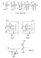
- FIG. 1 shows a number of examples of the heretofore taken countermeasure.
- Fig. 1 (a) shows the case where no measure is taken for an input circuit INC.
- a method of serially inserting a resistor R on the side of an input circuit INC within an IC a method of adding a diode D in parallel to the input circuit INC, or a method of adding a series resistor R and a parallel diode D in combination, has been employed. More particularly, Fig.
- the parasitic junction diode DI would necessarily have its positive pole connected to the ground potential and its negative pole connected to the collector. Since this parasitic diode DI has a high breakdown voltage and since its terminal voltage is suppressed to a low value after actuation of the transistor DI, the parasitic diode DI can be disregarded upon understanding the operation of the protective circuit 20 according to the present invention.
- the CEO structure transistor has a very strong durability against static electricity because heat generation caused by power dissipation within an element is far less for the latter. Since the quantity of heat generated within an element is mostly due to the heat generation at the B-C junction ( - 20 V) rather than at the B-E junction ( ⁇ 1 V), the durability against static electricity is determined by the area of the B -C junction.
- a junction area of a B-C diode and a B-C junction area of a CEO structure transistor is the same, then the CEO structure transistor has a far stronger durability against static electricity.
- it is intended to realize a durability against static electricity compatible to that of a CEO structure transistor by utilizing a B-C diode then it is compelled to disperse heat generation by enlarging the B-C junction area..
- a B-C junction area that is 5 times as large as that of the CEO structure transistor is necessitated, and even if the practical values of the parameters BP, V ON , r C , r b and r e in the transistor characteristics are taken into consideration in the protecting process, a B-C junction area that is 2 ⁇ 4 times as large as that of the CEO structure transistor is necessitated.
- the used of a B-C diode is disadvantageous in view of the size of the protective
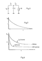
- a further improvement of the heretofore known electrostatic protective element for overcoming the above- described shortcomings of the E-B junction or C-B junction diode is the use of the base-opened C-E structure (CEO structure) transistor according to the present invention.
- C-E structure CEO structure
- a C-E breakdown point of a transistor is lower than a breakdown point of the C-B junction of the same transistor, and moreover a voltage-current characteristic of the C-E junction has a negative resistance. Therefore, the eventual C-E voltage after breakdown has a fairly low value.
- a monolithic IC having excellent quality in which electrostatic destruction would hardly occur can be provided by applying the CEO structure of the transistor that has a strong durability against electrostatic destruction and a large capability of absorbing electrostatic energy, to a protective element against electrostatic destruction.
- the initial-breakdown point becomes approximately equal to that of the C-B junction, so that it can well meet the rating input withstand voltage value, and further, since the eventual voltage after breakdown is exactly identical to that in the case of the CEO structure, with regard to the protective effect against electrostatic rupture, the protective circuit shown in Fig. 9 is quite the same as the transistor having the CEO structure.
Landscapes
- Semiconductor Integrated Circuits (AREA)
- Bipolar Integrated Circuits (AREA)
Applications Claiming Priority (2)
| Application Number | Priority Date | Filing Date | Title |
|---|---|---|---|
| JP8162480A JPS577151A (en) | 1980-06-17 | 1980-06-17 | Monolithic ic circuit |
| JP81624/80 | 1980-06-17 |
Publications (3)
| Publication Number | Publication Date |
|---|---|
| EP0042581A2 true EP0042581A2 (fr) | 1981-12-30 |
| EP0042581A3 EP0042581A3 (en) | 1983-09-28 |
| EP0042581B1 EP0042581B1 (fr) | 1986-12-30 |
Family
ID=13751477
Family Applications (1)
| Application Number | Title | Priority Date | Filing Date |
|---|---|---|---|
| EP81104648A Expired EP0042581B1 (fr) | 1980-06-17 | 1981-06-16 | Circuit intégré |
Country Status (3)
| Country | Link |
|---|---|
| EP (1) | EP0042581B1 (fr) |
| JP (1) | JPS577151A (fr) |
| DE (1) | DE3175781D1 (fr) |
Cited By (11)
| Publication number | Priority date | Publication date | Assignee | Title |
|---|---|---|---|---|
| EP0144208A1 (fr) * | 1983-11-30 | 1985-06-12 | Fujitsu Limited | Circuit de protection pour un dispositif à semi-conducteur |
| EP0136868A3 (en) * | 1983-09-22 | 1987-02-04 | Fujitsu Limited | Semiconductor device with protective elements |
| GB2179494B (en) * | 1985-08-09 | 1989-07-26 | Plessey Co Plc | Protection structures for integrated circuits |
| US4875130A (en) * | 1988-07-06 | 1989-10-17 | National Semiconductor Corporation | ESD low resistance input structure |
| US4904887A (en) * | 1982-06-30 | 1990-02-27 | Fujitsu Limited | Semiconductor integrated circuit apparatus |
| EP0480582A3 (en) * | 1990-09-10 | 1992-07-22 | Fujitsu Limited | A semiconductor device with a protective element |
| US5247201A (en) * | 1990-02-15 | 1993-09-21 | Siemens Aktiengesellschaft | Input protection structure for integrated circuits |
| US5272097A (en) * | 1992-04-07 | 1993-12-21 | Philip Shiota | Method for fabricating diodes for electrostatic discharge protection and voltage references |
| WO1996008801A3 (fr) * | 1994-09-13 | 1996-07-18 | Square D Co | Module de liaison de donnees pour des systemes de commande a multiplexage temporel |
| US5591661A (en) * | 1992-04-07 | 1997-01-07 | Shiota; Philip | Method for fabricating devices for electrostatic discharge protection and voltage references, and the resulting structures |
| US5818088A (en) * | 1995-09-11 | 1998-10-06 | Analog Devices, Inc. | Electrostatic discharge protection network and method |
Family Cites Families (6)
| Publication number | Priority date | Publication date | Assignee | Title |
|---|---|---|---|---|
| US3739238A (en) * | 1969-09-24 | 1973-06-12 | Tokyo Shibaura Electric Co | Semiconductor device with a field effect transistor |
| US3746946A (en) * | 1972-10-02 | 1973-07-17 | Motorola Inc | Insulated gate field-effect transistor input protection circuit |
| NL176322C (nl) * | 1976-02-24 | 1985-03-18 | Philips Nv | Halfgeleiderinrichting met beveiligingsschakeling. |
| JPS52139384A (en) * | 1976-05-18 | 1977-11-21 | Toshiba Corp | Semiconductor device |
| JPS5358777A (en) * | 1976-11-06 | 1978-05-26 | Mitsubishi Electric Corp | Semiconductor device |
| JPS5580350A (en) * | 1978-12-13 | 1980-06-17 | Fujitsu Ltd | Semiconductor integrated circuit |
-
1980
- 1980-06-17 JP JP8162480A patent/JPS577151A/ja active Pending
-
1981
- 1981-06-16 EP EP81104648A patent/EP0042581B1/fr not_active Expired
- 1981-06-16 DE DE8181104648T patent/DE3175781D1/de not_active Expired
Cited By (15)
| Publication number | Priority date | Publication date | Assignee | Title |
|---|---|---|---|---|
| US4904887A (en) * | 1982-06-30 | 1990-02-27 | Fujitsu Limited | Semiconductor integrated circuit apparatus |
| EP0136868A3 (en) * | 1983-09-22 | 1987-02-04 | Fujitsu Limited | Semiconductor device with protective elements |
| US4918563A (en) * | 1983-09-22 | 1990-04-17 | Fujitsu Limited | ECL gate array semiconductor device with protective elements |
| EP0144208A1 (fr) * | 1983-11-30 | 1985-06-12 | Fujitsu Limited | Circuit de protection pour un dispositif à semi-conducteur |
| GB2179494B (en) * | 1985-08-09 | 1989-07-26 | Plessey Co Plc | Protection structures for integrated circuits |
| US4875130A (en) * | 1988-07-06 | 1989-10-17 | National Semiconductor Corporation | ESD low resistance input structure |
| US5247201A (en) * | 1990-02-15 | 1993-09-21 | Siemens Aktiengesellschaft | Input protection structure for integrated circuits |
| EP0480582A3 (en) * | 1990-09-10 | 1992-07-22 | Fujitsu Limited | A semiconductor device with a protective element |
| US5648676A (en) * | 1990-09-10 | 1997-07-15 | Fujitsu Limited | Semiconductor device with protective element |
| US5670885A (en) * | 1990-09-10 | 1997-09-23 | Fujitsu Limited | Semiconductor device |
| US5272097A (en) * | 1992-04-07 | 1993-12-21 | Philip Shiota | Method for fabricating diodes for electrostatic discharge protection and voltage references |
| US5426322A (en) * | 1992-04-07 | 1995-06-20 | Shiota; Philip | Diodes for electrostatic discharge protection and voltage references |
| US5591661A (en) * | 1992-04-07 | 1997-01-07 | Shiota; Philip | Method for fabricating devices for electrostatic discharge protection and voltage references, and the resulting structures |
| WO1996008801A3 (fr) * | 1994-09-13 | 1996-07-18 | Square D Co | Module de liaison de donnees pour des systemes de commande a multiplexage temporel |
| US5818088A (en) * | 1995-09-11 | 1998-10-06 | Analog Devices, Inc. | Electrostatic discharge protection network and method |
Also Published As
| Publication number | Publication date |
|---|---|
| EP0042581B1 (fr) | 1986-12-30 |
| JPS577151A (en) | 1982-01-14 |
| DE3175781D1 (en) | 1987-02-05 |
| EP0042581A3 (en) | 1983-09-28 |
Similar Documents
| Publication | Publication Date | Title |
|---|---|---|
| US5276582A (en) | ESD protection using npn bipolar transistor | |
| US6271999B1 (en) | ESD protection circuit for different power supplies | |
| US6512662B1 (en) | Single structure all-direction ESD protection for integrated circuits | |
| US5721656A (en) | Electrostatc discharge protection network | |
| CN107528304B (zh) | 瞬态电压保护电路、装置和方法 | |
| US5521783A (en) | Electrostatic discharge protection circuit | |
| US5751525A (en) | EOS/ESD Protection circuit for an integrated circuit with operating/test voltages exceeding power supply rail voltages | |
| EP0324185B1 (fr) | Circuit de protection d'entrée pour dispositif semi-conducteur MOS | |
| US6657835B2 (en) | ESD protection circuit for mixed-voltage I/O by using stacked NMOS transistors with substrate triggering technique | |
| EP0352896A2 (fr) | Circuit de protection contre ESD pour des processus bipolaires | |
| US6442008B1 (en) | Low leakage clamp for E.S.D. protection | |
| US5336908A (en) | Input EDS protection circuit | |
| US6400204B1 (en) | Input stage ESD protection for an integrated circuit | |
| US5675469A (en) | Integrated circuit with electrostatic discharge (ESD) protection and ESD protection circuit | |
| US6215135B1 (en) | Integrated circuit provided with ESD protection means | |
| US6385116B2 (en) | Semiconductor integrated device | |
| EP0042581B1 (fr) | Circuit intégré | |
| US4839768A (en) | Protection of integrated circuits from electrostatic discharges | |
| US4131928A (en) | Voltage clamp device for monolithic circuits | |
| EP1423898B1 (fr) | Dispositif de protection contre les pointes de tension d'un circuit integre | |
| TWI877291B (zh) | 靜電放電保護器件及其方法,以及觸發整流器 | |
| US5138413A (en) | Piso electrostatic discharge protection device | |
| US6529059B1 (en) | Output stage ESD protection for an integrated circuit | |
| EP0472592A1 (fr) | Structure et dispositif de protection muni d'un redresseur au silicium commande a basse tension de declenchement. | |
| JPH0327566A (ja) | サージ保護装置 |
Legal Events
| Date | Code | Title | Description |
|---|---|---|---|
| PUAI | Public reference made under article 153(3) epc to a published international application that has entered the european phase |
Free format text: ORIGINAL CODE: 0009012 |
|
| AK | Designated contracting states |
Designated state(s): DE GB |
|
| PUAL | Search report despatched |
Free format text: ORIGINAL CODE: 0009013 |
|
| AK | Designated contracting states |
Designated state(s): DE GB |
|
| RAP1 | Party data changed (applicant data changed or rights of an application transferred) |
Owner name: NEC CORPORATION |
|
| 17P | Request for examination filed |
Effective date: 19831108 |
|
| GRAA | (expected) grant |
Free format text: ORIGINAL CODE: 0009210 |
|
| AK | Designated contracting states |
Kind code of ref document: B1 Designated state(s): DE GB |
|
| REF | Corresponds to: |
Ref document number: 3175781 Country of ref document: DE Date of ref document: 19870205 |
|
| PLBE | No opposition filed within time limit |
Free format text: ORIGINAL CODE: 0009261 |
|
| STAA | Information on the status of an ep patent application or granted ep patent |
Free format text: STATUS: NO OPPOSITION FILED WITHIN TIME LIMIT |
|
| 26N | No opposition filed | ||
| PGFP | Annual fee paid to national office [announced via postgrant information from national office to epo] |
Ref country code: GB Payment date: 19940616 Year of fee payment: 14 |
|
| PGFP | Annual fee paid to national office [announced via postgrant information from national office to epo] |
Ref country code: DE Payment date: 19940824 Year of fee payment: 14 |
|
| PG25 | Lapsed in a contracting state [announced via postgrant information from national office to epo] |
Ref country code: GB Effective date: 19950616 |
|
| GBPC | Gb: european patent ceased through non-payment of renewal fee |
Effective date: 19950616 |
|
| PG25 | Lapsed in a contracting state [announced via postgrant information from national office to epo] |
Ref country code: DE Effective date: 19960301 |