EP0042777A1 - Logischer Inverter und Operator mit mehreren Ausgängen, wobei wenigstens ein Feldeffekttransistor mit niedriger Schwelle verwendet wird - Google Patents
Logischer Inverter und Operator mit mehreren Ausgängen, wobei wenigstens ein Feldeffekttransistor mit niedriger Schwelle verwendet wird Download PDFInfo
- Publication number
- EP0042777A1 EP0042777A1 EP81400906A EP81400906A EP0042777A1 EP 0042777 A1 EP0042777 A1 EP 0042777A1 EP 81400906 A EP81400906 A EP 81400906A EP 81400906 A EP81400906 A EP 81400906A EP 0042777 A1 EP0042777 A1 EP 0042777A1
- Authority
- EP
- European Patent Office
- Prior art keywords
- terminal
- branch
- input
- output
- transistor
- Prior art date
- Legal status (The legal status is an assumption and is not a legal conclusion. Google has not performed a legal analysis and makes no representation as to the accuracy of the status listed.)
- Granted
Links
- 230000005669 field effect Effects 0.000 title claims abstract description 12
- 238000010586 diagram Methods 0.000 abstract description 19
- 239000008186 active pharmaceutical agent Substances 0.000 abstract description 7
- JBRZTFJDHDCESZ-UHFFFAOYSA-N AsGa Chemical compound [As]#[Ga] JBRZTFJDHDCESZ-UHFFFAOYSA-N 0.000 abstract description 3
- 229910001218 Gallium arsenide Inorganic materials 0.000 abstract description 3
- 235000021183 entrée Nutrition 0.000 description 19
- 238000000034 method Methods 0.000 description 5
- 230000009467 reduction Effects 0.000 description 4
- 238000012550 audit Methods 0.000 description 3
- 239000002131 composite material Substances 0.000 description 3
- 239000006185 dispersion Substances 0.000 description 3
- 238000004519 manufacturing process Methods 0.000 description 3
- 238000001465 metallisation Methods 0.000 description 3
- 239000003795 chemical substances by application Substances 0.000 description 2
- 230000000295 complement effect Effects 0.000 description 2
- 230000004044 response Effects 0.000 description 2
- 239000002699 waste material Substances 0.000 description 2
- 230000008901 benefit Effects 0.000 description 1
- 239000000470 constituent Substances 0.000 description 1
- 238000010276 construction Methods 0.000 description 1
- 238000000151 deposition Methods 0.000 description 1
- 230000000694 effects Effects 0.000 description 1
- 238000005516 engineering process Methods 0.000 description 1
- 230000003628 erosive effect Effects 0.000 description 1
- 230000003993 interaction Effects 0.000 description 1
- 230000002452 interceptive effect Effects 0.000 description 1
- 230000008520 organization Effects 0.000 description 1
- 230000003071 parasitic effect Effects 0.000 description 1
- 239000004065 semiconductor Substances 0.000 description 1
Images




Classifications
-
- H—ELECTRICITY
- H03—ELECTRONIC CIRCUITRY
- H03K—PULSE TECHNIQUE
- H03K19/00—Logic circuits, i.e. having at least two inputs acting on one output; Inverting circuits
- H03K19/02—Logic circuits, i.e. having at least two inputs acting on one output; Inverting circuits using specified components
- H03K19/08—Logic circuits, i.e. having at least two inputs acting on one output; Inverting circuits using specified components using semiconductor devices
- H03K19/094—Logic circuits, i.e. having at least two inputs acting on one output; Inverting circuits using specified components using semiconductor devices using field-effect transistors
- H03K19/09421—Diode field-effect transistor logic
-
- H—ELECTRICITY
- H03—ELECTRONIC CIRCUITRY
- H03K—PULSE TECHNIQUE
- H03K19/00—Logic circuits, i.e. having at least two inputs acting on one output; Inverting circuits
- H03K19/02—Logic circuits, i.e. having at least two inputs acting on one output; Inverting circuits using specified components
- H03K19/08—Logic circuits, i.e. having at least two inputs acting on one output; Inverting circuits using specified components using semiconductor devices
- H03K19/094—Logic circuits, i.e. having at least two inputs acting on one output; Inverting circuits using specified components using semiconductor devices using field-effect transistors
- H03K19/0952—Logic circuits, i.e. having at least two inputs acting on one output; Inverting circuits using specified components using semiconductor devices using field-effect transistors using Schottky type FET MESFET
Definitions
- the invention relates to a fast logic inverter, with a single power source, using a field effect transistor with low threshold voltage called "quasi-normally blocked". It also concerns the logical operators with several outputs, built from this inverter, and performing more or less complex logic functions. It can be implemented in integrated circuits.
- normally conductive field effect transistors and normally blocked transistors are known.
- the former are blocked by depletion, requiring a double-polarity power supply and also having the drawback of consuming electrical current in the quiescent state.
- the second allow the current to flow when an appropriate voltage is applied to the control grid: they do not require a double polarity supply and are more economical, but on the other hand difficult to achieve, because of the very thin thickness of the conduction channel giving rise to a large amount of manufacturing waste.
- a third category of field effect transistors which is intermediate between the two preceding ones while approaching the second, is constituted by the quasi-normally blocked transistors: they are blocked for a threshold voltage VT which can be positive or negative , which means that we admit a certain dispersion in the collective manufacturing of these transistors which is for example the following: - 0.4 V T 0.2 volt.
- the invention aims to create a new family of logical operators having, or capable of presenting, several inputs and also several independent outputs, that is to say to achieve a "convergent-divergent" logic.
- a middle branch comprising in series a second resistive load, one terminal of which is connected to ground, a diode supplemented by an additional diode in series in the case where the input branch itself comprises a diode, and a transistor having its drain connected to said pole, its source connected to a diode of the middle branch, its gate connected to the terminal of the first resistive load not connected audit pole.
- an output branch comprising a transistor having its source to ground, its gate connected to the terminal of the second resistive load not connected to ground and its drain connected to an output terminal intended to deliver logic signals between this terminal and said pole, the diode (s) of the middle branch being conducting (s) in the direction from said pole to ground.
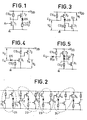
- FIG. 1 there is shown a logic inverter whose input A is connected to the gate of a transistor T 1 which is of the quasi-normally blocked type.
- This transistor has its source to ground, its drain connected to a point I connected itself to the hot point corresponding to a pole (positive in this example) of a source V DD through a resistive load CS 1 .
- the example chosen corresponds to the case of the n-channel transistor. For a p channel, the polarities must be reversed.
- Point 1 is connected to the gate of a transistor T 2 of the same type as T 1 .
- the transistor T 2 has its drain connected to the pole + V DD , its source has a diode DS, conducting in the direction going from + V DD to ground. The return to ground is carried out through a resistive load CS 2 .
- the output A of the inverter is taken between DS and CS 2 .
- FIG. 2 shows such a chain, in which the output of an inverter is connected to the input of the next inverter.
- the closed contour 21 delimits the inverter of FIG. 1, with its terminals E l and S 1 designating the terminals A and A, of the diagram of this basic inverter
- the closed contour 22 delimits an inverter derived from the basic inverter, from terminals E 2 (input) and S 2 (output).
- FIG. 3 shows this derivative inverter.
- inverter which corresponds to that which has been defined above as a variant of the invention, namely the inverter which does not have a diode in the input branch or half-branch.
- E 2 input terminal
- the resistive loads CS 1 and CS 2 , the transistor T 2 , the diode DS occupy places which are the counterparts of those of FIG. 1.
- the transistor T 1 in a half output branch there is the transistor T 1 .
- This inverter will be designated hereinafter as an "open drain outlet inverter" because of the location of the outlet S 2 .
- the voltage output signals V S between S 2 and pole + V DD must be collected.
- this inverter has the same compatibility properties as the basic inverter, that is to say that it is capable of forming, like the inverter in FIG. 1, a chain of operators which does not differ of the chain of FIG. 2 only by the entry and exit conditions. Indeed at points E 2 and S 2 , it suffices to respect the logic levels observable in the chain of FIG. 2, to obtain a succession of compatible signals.
- the closed contour 23 of FIG. 2 is also considered, delimiting an input E 3 and output S 3 inverter, which differs from the inverter of FIG. 1, by a reverse arrangement of the branches entry and exit.
- This inverter can be used in the construction of logical operators with several inputs described in the request for aforementioned patent.
- closed contour 24 of FIG. 2 defines a basic inverter according to the definition of the invention given above.
- inverter with output on open source As in FIG. 3, the references of the members of FIG. 1 have been used to designate those of this inverter, of input E4 and of output S 4 , (fig. 4) hereinafter called “inverter with output on open source. “due to the position of the output terminal on the source of the output transistor.
- This basic inverter has an input in which the signals are applied between the terminal E4 and the pole + V DD , an input branch with a diode D, a resistive load designated by C5 2 by analogy with the diagram in Figure 1 , a middle branch with another resistive load, here CS 1 , and a transistor T 1 , finally an output branch with a transistor T 2 , the source of which is separated from ground to constitute an output terminal S 4 .
- FIG. 5 A variant of the inverter of Figure 3 is shown in Figure 5 which is deduced from the diagram of Figure 3 by inserting two additional diodes, one D 51 between the input, designated by E5, and point I of standard diagram (FIG. 1), the other D 52 being in series between the diode DS of the diagram in FIG. 3 and the source of the transistor T 2 .
- the inverter in Figure 5 is “compatible". Since the diode D 51 is added to create a "AND" type function at the input of the logic operator, the diode D 52 is only added to compensate for the shift in the input level provided by the diode D 51 . However, the supply of this inverter requires a slightly higher voltage supply due to the presence of the diode.
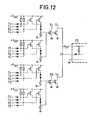
- Figure 7 gives the equivalent logic diagram of the operator in Figure 6: OR - AND - OR NOT (OR - AND - NOR) with n independent outputs.
- Figure 9 gives the logic diagram equivalent to the operator of Figure 8: AND - OR - AND NOT (AND - OR - NAND).
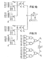
- Figure 11 gives the equivalent logic diagram of this operator. We see that, depending on the output used, we have in the case of outputs S ' l and S' 2 not wired, the complex function at three levels:
- each of the independent outputs can be adapted in size to the capacitive load that it controls, therefore according to the fanout. This advantage is important for optimizing overall performance in a complex circuit.
- This operator similar to the previous one, also has 16 inputs, independent outputs S ' 1 and S' 2 and outputs S 1 and S 2 wired at a point Z.
- This operator has a supply compatibility with that of FIG. 10 and the same number of elements to be crossed (a diode and two gate-source junctions) therefore a speed of the same order.
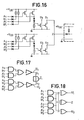
- FIGS 14 and 15 give the equivalent logic diagrams of the operator of Figure 13.
- AND - OR NOT (AND - NOR) for output Z of the door with 8 inputs and for outputs S ' 1 and S' 2 (of doors with four inputs).
- This operator was constructed, FIG. 19, from two inverters of the type represented in FIG. 4, of inputs 1 and 2 on the one hand, 3 and 4 on the other hand, whose outputs are combined to constitute a single output S .
- the homologous resistive charges of the two inverters have been designated by CS ' 1 and CS " 1 , and likewise for the transistors T 1 (T' 1 , T" 1 ) and T 2 (T ' 2 , T “ 2 ), these the latter having their sources connected together to form the output S. This produces a "wired OR".
- Figures 20 and 21 give equivalent logic diagrams which differ according to the way of supplying inputs 1, 2, 3 and 4 by signals A and B or their complements.
- a complete adder is constituted, FIG. 22, using logical operators identical to that of the last example (0 1 and 0 3 ) or analogous (0 2 ) to this one.
- the operator 0 2 differs from that of FIG. 19 by the fact that in the inverter of this figure a transistor is added having its drain at the pole + V DD , its open source (output of type S ') and its connected gate to that of one of the operator's output transistors.
Landscapes
- Engineering & Computer Science (AREA)
- Power Engineering (AREA)
- Physics & Mathematics (AREA)
- Computer Hardware Design (AREA)
- Computing Systems (AREA)
- General Engineering & Computer Science (AREA)
- Mathematical Physics (AREA)
- Logic Circuits (AREA)
- Electronic Switches (AREA)
Applications Claiming Priority (2)
| Application Number | Priority Date | Filing Date | Title |
|---|---|---|---|
| FR8013964 | 1980-06-24 | ||
| FR8013964A FR2485832A1 (fr) | 1980-06-24 | 1980-06-24 | Inverseur logique, et operateur a plusieurs sorties derive de cet inverseur, utilisant au moins un transistor a effet de champ a faible tension de seuil |
Publications (2)
| Publication Number | Publication Date |
|---|---|
| EP0042777A1 true EP0042777A1 (de) | 1981-12-30 |
| EP0042777B1 EP0042777B1 (de) | 1984-09-12 |
Family
ID=9243442
Family Applications (1)
| Application Number | Title | Priority Date | Filing Date |
|---|---|---|---|
| EP81400906A Expired EP0042777B1 (de) | 1980-06-24 | 1981-06-05 | Logischer Inverter und Operator mit mehreren Ausgängen, wobei wenigstens ein Feldeffekttransistor mit niedriger Schwelle verwendet wird |
Country Status (6)
| Country | Link |
|---|---|
| US (1) | US4485316A (de) |
| EP (1) | EP0042777B1 (de) |
| JP (1) | JPS5739626A (de) |
| DE (1) | DE3165984D1 (de) |
| FR (1) | FR2485832A1 (de) |
| NO (1) | NO153870C (de) |
Cited By (9)
| Publication number | Priority date | Publication date | Assignee | Title |
|---|---|---|---|---|
| EP0053664A1 (de) * | 1980-12-05 | 1982-06-16 | International Business Machines Corporation | Integriertes logisches Tor |
| EP0110701A3 (en) * | 1982-11-27 | 1985-01-09 | Hitachi, Ltd. | Input buffer circuit |
| EP0085569A3 (en) * | 1982-02-01 | 1985-01-09 | Sperry Corporation | Gallium arsenide logic circuit |
| EP0203384A3 (de) * | 1985-04-29 | 1987-03-04 | Honeywell Inc. | Vielfacheingangsschaltung für Feldeffekttransistoren |
| US4703205A (en) * | 1985-07-26 | 1987-10-27 | Rockwell International Corporation | Uncompensated and compensated gallium arsenide input receivers |
| US4791322A (en) * | 1987-05-19 | 1988-12-13 | Gazelle Microcircuits, Inc. | TTL compatible input buffer |
| US4912745A (en) * | 1987-05-19 | 1990-03-27 | Gazelle Microcircuits, Inc. | Logic circuit connecting input and output signal lines |
| EP0307831A3 (de) * | 1987-09-14 | 1990-12-27 | Hughes Aircraft Company | Hochgeschwindigkeitsaddierer |
| FR2716586A1 (fr) * | 1994-02-23 | 1995-08-25 | Bull Sa | Porte ou-Exclusif intégrée dans un semi-conducteur III-V. |
Families Citing this family (10)
| Publication number | Priority date | Publication date | Assignee | Title |
|---|---|---|---|---|
| FR2528596A1 (fr) * | 1982-06-09 | 1983-12-16 | Labo Cent Telecommunicat | Cellule d'addition binaire a trois entrees a propagation rapide de la somme, realisee en circuit integre |
| JPS59191937A (ja) * | 1983-04-15 | 1984-10-31 | Nec Corp | 高速論理回路 |
| US4680484A (en) * | 1984-10-19 | 1987-07-14 | Trw Inc. | Wired-AND FET logic gate |
| US4725743A (en) * | 1986-04-25 | 1988-02-16 | International Business Machines Corporation | Two-stage digital logic circuits including an input switching stage and an output driving stage incorporating gallium arsenide FET devices |
| US4701646A (en) * | 1986-11-18 | 1987-10-20 | Northern Telecom Limited | Direct coupled FET logic using a photodiode for biasing or level-shifting |
| US4877976A (en) * | 1987-03-13 | 1989-10-31 | Gould Inc. | Cascade FET logic circuits |
| FR2612660B1 (fr) * | 1987-03-18 | 1990-10-19 | Hmida Hedi | Dispositif de calcul binaire |
| US4844563A (en) * | 1987-05-19 | 1989-07-04 | Gazelle Microcircuits, Inc. | Semiconductor integrated circuit compatible with compound standard logic signals |
| FR2653277A1 (fr) * | 1989-10-17 | 1991-04-19 | Thomson Composants Microondes | Circuit integre logique, a temps de basculement reglable. |
| CN113353150B (zh) * | 2021-06-29 | 2023-06-16 | 三一重机有限公司 | 具有防限位件断裂损坏功能的底盘、方法及作业机械 |
Family Cites Families (4)
| Publication number | Priority date | Publication date | Assignee | Title |
|---|---|---|---|---|
| US3969632A (en) * | 1971-07-06 | 1976-07-13 | Thomson-Csf | Logic circuits-employing junction-type field-effect transistors |
| FR2264434B1 (de) * | 1974-03-12 | 1976-07-16 | Thomson Csf | |
| US4300064A (en) * | 1979-02-12 | 1981-11-10 | Rockwell International Corporation | Schottky diode FET logic integrated circuit |
| FR2449369A1 (fr) * | 1979-02-13 | 1980-09-12 | Thomson Csf | Circuit logique comportant une resistance saturable |
-
1980
- 1980-06-24 FR FR8013964A patent/FR2485832A1/fr active Granted
-
1981
- 1981-06-05 EP EP81400906A patent/EP0042777B1/de not_active Expired
- 1981-06-05 DE DE8181400906T patent/DE3165984D1/de not_active Expired
- 1981-06-22 US US06/275,623 patent/US4485316A/en not_active Expired - Fee Related
- 1981-06-23 NO NO812145A patent/NO153870C/no unknown
- 1981-06-24 JP JP56098162A patent/JPS5739626A/ja active Pending
Non-Patent Citations (5)
| Title |
|---|
| IEE Proceedings - 1, Vol. 127, No. 5, Partie 1, Octobre 1980 Stevenage Herts (GB) NUZILLAT et al.: "Low Pinch-Off Voltage f.e.t. Logic (i.p.F.i.) l.s.i. Oriented Logic Approach Using Quasinormally off GaAs m.e.s.F.e.t.s." pages 287-295 *figures 3, 9b, 10, 10b; de page 287, colonne de droite, ligne k- page 291, colonne de gauche, ligne 29* * |
| IEEE International Solid State Circuit Conference, 14 Fevrier 1980 New York (US)R.C. EDEN et al.: "Multi-Level Logic Gate Implemtation in GaAs ICs using Schottky Diode-Fet Logic" pages 122-123 et 265-266 *figures 1, 4; en entier* * |
| IEEE Transaction on Electron Devices, Vol. ED-27, No. 6, Juin 1980 New York (US)G. NUZILLAT et al.: "Quasi-Normal by-off Mesfet Logic for High-Performance GaAsIC's" pages 1102-1109 *figures 3, 5; en entier* * |
| Proccedings of the IEEE, Vol. 67, No. 3, Mars 1979 New York (US) B.G. BOSCH: "Gigabit Electronics a Review" pages 340-379 *figure 64; page 365, colonne de gauche, lignes 30, 31* * |
| Supplement to the Jounal of the Japan Society of Applied Physics: Proceedings of the 6th Conference on Solid State Devices, Vol. 44, Tokyo 1974/1975 Tokyo (JP) SUZUKI et al.: "Logic Circuits with mu Gate Schottky Barrier Fets" pages 219-224*figures 2, 4; page 219, colonne de droite, ligne 23 - page 221: colonne de gauche, ligne 3* * |
Cited By (12)
| Publication number | Priority date | Publication date | Assignee | Title |
|---|---|---|---|---|
| EP0053664A1 (de) * | 1980-12-05 | 1982-06-16 | International Business Machines Corporation | Integriertes logisches Tor |
| EP0085569A3 (en) * | 1982-02-01 | 1985-01-09 | Sperry Corporation | Gallium arsenide logic circuit |
| EP0110701A3 (en) * | 1982-11-27 | 1985-01-09 | Hitachi, Ltd. | Input buffer circuit |
| EP0203384A3 (de) * | 1985-04-29 | 1987-03-04 | Honeywell Inc. | Vielfacheingangsschaltung für Feldeffekttransistoren |
| US4703205A (en) * | 1985-07-26 | 1987-10-27 | Rockwell International Corporation | Uncompensated and compensated gallium arsenide input receivers |
| US4791322A (en) * | 1987-05-19 | 1988-12-13 | Gazelle Microcircuits, Inc. | TTL compatible input buffer |
| GB2207317A (en) * | 1987-05-19 | 1989-01-25 | Gazelle Microcircuits Inc | Ttl compatible input buffer |
| US4912745A (en) * | 1987-05-19 | 1990-03-27 | Gazelle Microcircuits, Inc. | Logic circuit connecting input and output signal lines |
| GB2207317B (en) * | 1987-05-19 | 1992-01-29 | Gazelle Microcircuits Inc | Input level shifter circuit |
| EP0307831A3 (de) * | 1987-09-14 | 1990-12-27 | Hughes Aircraft Company | Hochgeschwindigkeitsaddierer |
| FR2716586A1 (fr) * | 1994-02-23 | 1995-08-25 | Bull Sa | Porte ou-Exclusif intégrée dans un semi-conducteur III-V. |
| EP0670634A1 (de) * | 1994-02-23 | 1995-09-06 | Bull S.A. | Eklusiv-ODER Gatter in einem III-V Halbleiter |
Also Published As
| Publication number | Publication date |
|---|---|
| NO153870C (no) | 1986-06-04 |
| DE3165984D1 (en) | 1984-10-18 |
| NO153870B (no) | 1986-02-24 |
| NO812145L (no) | 1981-12-28 |
| JPS5739626A (en) | 1982-03-04 |
| EP0042777B1 (de) | 1984-09-12 |
| FR2485832A1 (fr) | 1981-12-31 |
| US4485316A (en) | 1984-11-27 |
| FR2485832B1 (de) | 1984-07-13 |
Similar Documents
| Publication | Publication Date | Title |
|---|---|---|
| EP0042777B1 (de) | Logischer Inverter und Operator mit mehreren Ausgängen, wobei wenigstens ein Feldeffekttransistor mit niedriger Schwelle verwendet wird | |
| EP0041415B1 (de) | Schneller logischer Operator mit hoher Eingangsbelastbarkeit und komplexer logischer Funktion mit wenigstens zwei Feldeffekttransistoren mit niedrigem Schwellwert | |
| EP0362080B1 (de) | Monolithischer Zweiwegschalter mit MOS-Leistungstransistoren | |
| EP0080394B1 (de) | Bistabile Kippschaltung mit energieunabhängiger Haltbarkeit und statischer Rücksetzung | |
| EP0357528B1 (de) | MOS-Transistor und Anwendung bei einer Freilaufdiode | |
| CA2137340C (fr) | Arbre de portes logique ou - exclusif et multiplieur de frequence l'incorporant | |
| FR2644651A1 (fr) | Circuit de commande de transistor mos de puissance sur charge inductive | |
| FR2693327A1 (fr) | Circuit de commutation de haute tension. | |
| EP0409746A1 (de) | Integrierter VDMOS/Logikschaltkreis mit vertikalem Transistor vom Verarmungstyp und einer Zenerdiode | |
| EP0432058B1 (de) | Dynamische Isolierschaltung für integrierte Schaltungen | |
| EP0328465A1 (de) | Gate-Steuerschaltung eines MOS-Leistungstransistors im Schaltbetrieb | |
| EP0262013B1 (de) | Leseverstärker | |
| EP2784817A1 (de) | Verfahren zum Steuern einer integrierten Schaltung | |
| EP0237094A1 (de) | Vordiffundierte Gatterfeld-Halbleitervorrichtung für speziell hergestellte Schaltungen | |
| EP0359680B1 (de) | Integrierbare, aktive Diode | |
| FR2528596A1 (fr) | Cellule d'addition binaire a trois entrees a propagation rapide de la somme, realisee en circuit integre | |
| EP0865671B1 (de) | Normal leitender dual-thyristor | |
| EP0424222A1 (de) | Integrierte Logikschaltung mit einstellbaren Àbergangszeiten | |
| FR2760151A1 (fr) | Amplificateur-tampon de commande de bus | |
| EP0379454A1 (de) | Von einer Vorrichtung mit zwei symmetrischen Ladungspumpen gesteuerte Leistungs-MOS-Transistorschaltung | |
| FR2813698A1 (fr) | Cellule cache a masquage | |
| EP0187584B1 (de) | Logisches Koinzidenztor und dieses verwendende logische sequentielle Schaltungen | |
| EP2246886A1 (de) | Integrierter Schaltkreis, der mit einem großflächigen Schutz gegen elektrostatische Entladungen ausgestattet ist | |
| EP0073700A1 (de) | Logischer Schaltkreis mit hoher Eingangsbelastbarkeit und wenigstens einem Feldeffekttransistor mit niedriger Schwelle | |
| EP0709963B1 (de) | CMOS-Multiplexer für logische Variablen |
Legal Events
| Date | Code | Title | Description |
|---|---|---|---|
| PUAI | Public reference made under article 153(3) epc to a published international application that has entered the european phase |
Free format text: ORIGINAL CODE: 0009012 |
|
| AK | Designated contracting states |
Designated state(s): DE GB NL SE |
|
| 17P | Request for examination filed |
Effective date: 19820116 |
|
| GRAA | (expected) grant |
Free format text: ORIGINAL CODE: 0009210 |
|
| AK | Designated contracting states |
Designated state(s): DE GB NL SE |
|
| REF | Corresponds to: |
Ref document number: 3165984 Country of ref document: DE Date of ref document: 19841018 |
|
| PLBE | No opposition filed within time limit |
Free format text: ORIGINAL CODE: 0009261 |
|
| STAA | Information on the status of an ep patent application or granted ep patent |
Free format text: STATUS: NO OPPOSITION FILED WITHIN TIME LIMIT |
|
| 26N | No opposition filed | ||
| PGFP | Annual fee paid to national office [announced via postgrant information from national office to epo] |
Ref country code: SE Payment date: 19890526 Year of fee payment: 9 Ref country code: DE Payment date: 19890526 Year of fee payment: 9 |
|
| PGFP | Annual fee paid to national office [announced via postgrant information from national office to epo] |
Ref country code: GB Payment date: 19890531 Year of fee payment: 9 |
|
| PGFP | Annual fee paid to national office [announced via postgrant information from national office to epo] |
Ref country code: NL Payment date: 19890630 Year of fee payment: 9 |
|
| PG25 | Lapsed in a contracting state [announced via postgrant information from national office to epo] |
Ref country code: GB Effective date: 19900605 |
|
| PG25 | Lapsed in a contracting state [announced via postgrant information from national office to epo] |
Ref country code: SE Effective date: 19900606 |
|
| PG25 | Lapsed in a contracting state [announced via postgrant information from national office to epo] |
Ref country code: NL Effective date: 19910101 |
|
| GBPC | Gb: european patent ceased through non-payment of renewal fee | ||
| NLV4 | Nl: lapsed or anulled due to non-payment of the annual fee | ||
| PG25 | Lapsed in a contracting state [announced via postgrant information from national office to epo] |
Ref country code: DE Effective date: 19910301 |
|
| EUG | Se: european patent has lapsed |
Ref document number: 81400906.4 Effective date: 19910206 |