EP0043009A2 - Semiconductor controlled switch - Google Patents
Semiconductor controlled switch Download PDFInfo
- Publication number
- EP0043009A2 EP0043009A2 EP81104472A EP81104472A EP0043009A2 EP 0043009 A2 EP0043009 A2 EP 0043009A2 EP 81104472 A EP81104472 A EP 81104472A EP 81104472 A EP81104472 A EP 81104472A EP 0043009 A2 EP0043009 A2 EP 0043009A2
- Authority
- EP
- European Patent Office
- Prior art keywords
- zone
- fet
- conductivity type
- semiconductor body
- semiconductor switch
- Prior art date
- Legal status (The legal status is an assumption and is not a legal conclusion. Google has not performed a legal analysis and makes no representation as to the accuracy of the status listed.)
- Granted
Links
Images


Classifications
-
- H—ELECTRICITY
- H10—SEMICONDUCTOR DEVICES; ELECTRIC SOLID-STATE DEVICES NOT OTHERWISE PROVIDED FOR
- H10D—INORGANIC ELECTRIC SEMICONDUCTOR DEVICES
- H10D18/00—Thyristors
- H10D18/40—Thyristors with turn-on by field effect
-
- H—ELECTRICITY
- H10—SEMICONDUCTOR DEVICES; ELECTRIC SOLID-STATE DEVICES NOT OTHERWISE PROVIDED FOR
- H10D—INORGANIC ELECTRIC SEMICONDUCTOR DEVICES
- H10D18/00—Thyristors
- H10D18/241—Asymmetrical thyristors
-
- H—ELECTRICITY
- H10—SEMICONDUCTOR DEVICES; ELECTRIC SOLID-STATE DEVICES NOT OTHERWISE PROVIDED FOR
- H10D—INORGANIC ELECTRIC SEMICONDUCTOR DEVICES
- H10D18/00—Thyristors
- H10D18/60—Gate-turn-off devices
- H10D18/65—Gate-turn-off devices with turn-off by field effect
- H10D18/655—Gate-turn-off devices with turn-off by field effect produced by insulated gate structures
Definitions
- the present invention relates to a controllable semiconductor switch with a semiconductor body, comprising a thyristor structure with a first zone of the first conductivity type, which is planarly embedded in a second zone of the second conductivity type, containing a third zone of the first conductivity type and a fourth zone of the second conductivity type , further comprising an MIS-FET integrated into the semiconductor body, the source zone of which is of the first conductivity type and which is planarly embedded in a zone of the second conductivity type, with a control electrode which is arranged on an insulating layer lying on the surface of the semiconductor body and covers a first channel zone assigned to the FET, and with a cathode electrode on the semiconductor body.
- Such a semiconductor switch has been described for example in DE-OS 26 25 917.
- This semiconductor switch is a thyristor that can be switched off and a field-effect transistor (FET) is integrated in its semiconductor body.
- a control electrode which is insulated from the surface of the semiconductor body is provided for driving the FET.
- the FET is turned on and creates a short circuit between the cathode-side emitter zone and the cathode-side base zone. Then the thyristor current flows partly bypassing the emitter zone on the cathode side into the short circuits. The cargo this reduces carrier emissions from the cathode zone.
- the thyristor has another control electrode through which control current can be injected into the semiconductor body in a known manner. This control current is usually between 10 and 100 mA. Direct control by microprocessors or LSI circuits is therefore not an option.
- the semiconductor MIS-FETs which have recently become known belong to the semiconductor switches which can be controlled directly by microprocessors. However, these MIS-FETs have a relatively high switch-on resistance, which is higher the higher the voltage to be switched. With a MIS-FET for 500 V, for example, this switch-on resistance is between 1 and 5 ohms. At high current, a quite considerable power loss is therefore implemented in the transistor, which must be dissipated by cooling.
- the invention has for its object to develop a switchable semiconductor switch of the type mentioned so that it can be controlled almost without power and also has a very low on resistance.
- Zone 1 has a semiconductor body 1 which has a thyristor structure and an FET.
- the FET has a source zone 2 which is planarly embedded in a zone 3 of the opposite conductivity type.
- Zone 3 is in turn embedded in a third zone 4 of semiconductor body 1.
- Zone 3 therefore extends to the surface of the semiconductor body and is intended to form a conductive layer of the FET.
- the third zone 4 serves as the drain zone of the FET. In the exemplary embodiment, it is weakly n-doped, zone 3 is p-doped and zone 2 is heavily n-doped.
- the thyristor structure consists of a first zone 9, which is planarly embedded in a second zone 10.
- the second zone 10 is in turn planar embedded in third zone 4, which belongs together to the thyristor structure and the FET.
- the fourth zone of the thyristor structure is formed by zone 6.
- the first zone 9 is the cathode-side emitter zone
- zone 10 is the cathode-side base zone
- zone 4 is the anode-side base zone
- zone 6 is the anode-side emitter zone.
- the doping of the zones mentioned is n + pn - p + in the exemplary embodiment.
- a heavily n-doped region 5 can also be provided between zones 4 and 6, the function of which will be explained further below.
- Zone 10 extends to the surface of the semiconductor body and is intended to form a second channel zone.
- the surface of the semiconductor body is provided with an insulating layer 8, for example made of SiO 2 , on which a control electrode 11 is arranged.
- the control electrode 11 covers the channel zones 13, 14 of the zones 3 and 10 and the area of the zone 4 which occurs between the channel zones on the surface of the semiconductor body.
- the source zone 2 is contacted with an electrode 7 which takes over the function of a cathode electrode. It can also contact Zone 3 of the FET at the same time.
- a resistance R g is also drawn in between zones 3 and 10, by means of which zone 10 is set to a fixed potential. This resistance can either be represented externally or by means of a web of the same conductivity type connecting zones 10 and 3.
- the control electrode 11 is at the same potential as the cathode electrode 7.
- the switch is biased in the blocking direction (forward direction) and the pn junction between zones 3 and 4 is blocked.
- a space charge zone is formed, the boundary of which is designated by 12. If a positive voltage + Ug is applied to the electrode 11 (FIG. 2), In this way, inversion layers are formed in the channel zones 13, 14, which represent n-conducting channels between zones 2 and 4 or 4 and 9.
- an enrichment layer 15 is formed from negative charge carriers, so that a well conductive, purely ohmic connection is established between zones 2 and 9.
- zone 9 is practically at cathode potential. This can start an emission of negative charge carriers from zone 9 into zone 4, which causes an emission of positive charge carriers from zone 6. This process continues until the pn junction between zones 10 and 4 is polarized in the forward direction and the thyristor structure ignites.
- the control voltage is removed.
- Layer 15 thus dissolves and the inversion layers in channel zones 13 and 14 disappear.
- the current flow to the thyristor structure is thus interrupted and it changes to the blocked state.
- the positive and negative charge carriers stored in the semiconductor body disappear through recombination.
- the recombination speed can be increased by installing heavily n-doped zone 5 between zones 4 and 6.
- the Dotie Zones 5 and 6 can be the same height. If a longer decay time of the current can be accepted, zone 5 is unnecessary, which also has the advantage that the semiconductor switch can also block higher voltages in the reverse direction.
- FIG. 3 shows a semiconductor switch which can be switched off and which differs from that described in FIGS. 1 and 2 by its lateral structure.
- the same or functionally identical parts as in Fig. 1 and 2 are designated the same.
- the anode-side emitter zone (4th zone) of the thyristor structure bears the reference number 16 and lies on that surface of the semiconductor body 1 which bears the cathode contact 7. It is expediently arranged on the side of zones 9 and 10 facing away from FET 2, 3, 4.
- Zone 16 like the other zones, is embedded planarly in the surface of semiconductor body 1.
- Zone 16 carries an anode contact 18. It can be surrounded by a heavily doped zone 17, which has the same function as zone 5 according to FIGS. 1 and 2.
- the on-resistance of an embodiment of the semiconductor switch described which was designed for 500 V and 10 A, for example, was only a few tenths of an ohm.
- the on-resistance is thus about an order of magnitude lower than that of a field effect transistor.
Landscapes
- Thyristors (AREA)
Abstract
Die Erfindung bezieht sich auf einen steuerbaren Halbleiterschalter. Der Einschaltwiderstand von für hohe Spannungen ausgelegten MIS-FET liegt relativ hoch. Es wird ein steuerbarer Halbleiterschalter angegeben, bei dem eine Thyristorstruktur mit einem MIS-FET zusammenwirkt. Die Katodenelektrode (7) kontaktiert den FET (2, 3, 4), während die Thyristorstruktur (9, 10, 4, 6) eine Kanalzone (13), aber keinen Katodenkontakt hat. Der Strom wird durch Anlegen einer Gate-Spannung gesteuert, die sowohl die Kanalzone (13) der Thyristorstruktur als auch die Kanalzone (14) des FET öffnet. Die Strom-Spannungscharakteristik gleicht einem Thyristor, der Einschaltwiderstand ist gering. Der Halbleiterschalter wird einfach durch Abschalten der Gate-Spannung gesperrt. Die Erfindung ist zum Beispiel bei Motorsteuerungen anwendbar.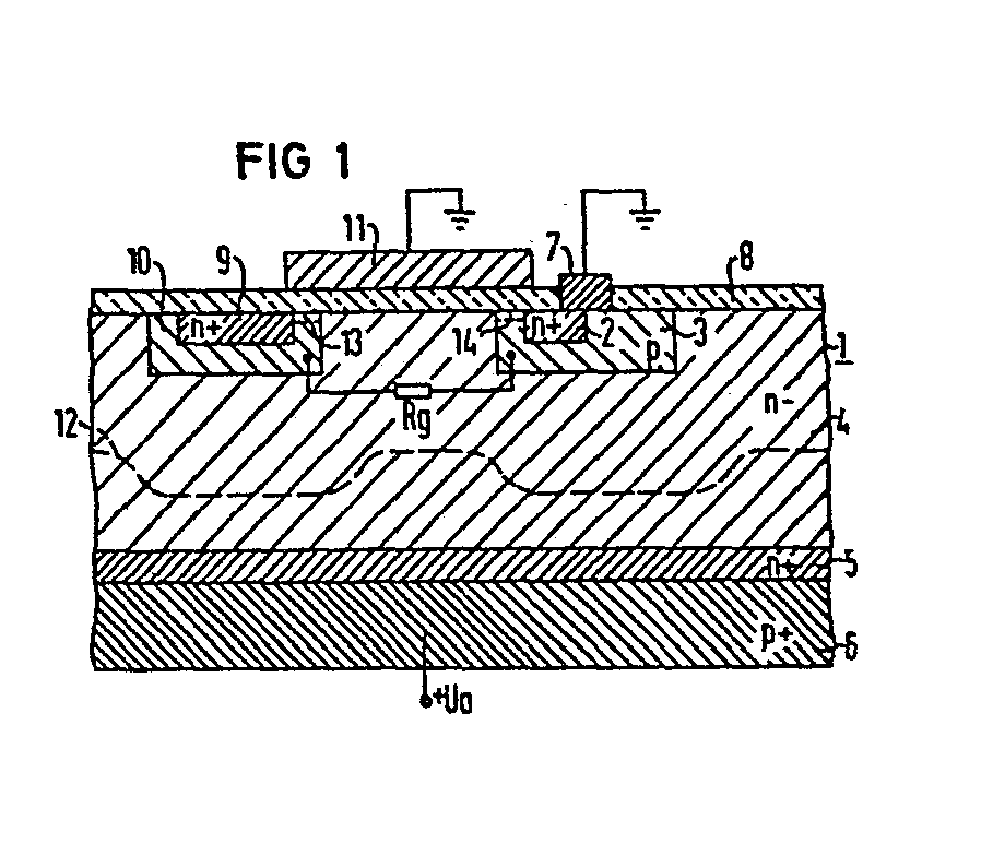
Description
Die vorliegende Erfindung bezieht sich auf einen steuerbaren Halbleiterschalter mit einem Halbleiterkörper, enthaltend eine Thyristorstruktur mit einer ersten Zone vom ersten Leitfähigkeitstyp, die planar in eine zweite Zone vom zweiten Leitfähigkeitstyp eingebettet ist, enthaltend eine dritte Zone vom ersten Leitfähigkeitstyp und eine vierte Zone vom zweiten Leitfähigkeitstyp,
enthaltend weiter einen in den Halbleiterkörper integrierten MIS-FET, dessen Source-Zone vom ersten Leitfähigkeitstyp ist und die planar in eine Zone vom zweiten Leitfähigkeitstyp eingebettet ist,
mit einer Steuerelektrode, die auf einer auf der Oberfläche des Halbleiterkörpers liegenden Isolierschicht angeordnet ist und eine dem FET zugeordnete erste Kanalzone überdeckt,
und mit einer Katodenelektrode auf dem Halbleiterkörper.The present invention relates to a controllable semiconductor switch with a semiconductor body, comprising a thyristor structure with a first zone of the first conductivity type, which is planarly embedded in a second zone of the second conductivity type, containing a third zone of the first conductivity type and a fourth zone of the second conductivity type ,
further comprising an MIS-FET integrated into the semiconductor body, the source zone of which is of the first conductivity type and which is planarly embedded in a zone of the second conductivity type,
with a control electrode which is arranged on an insulating layer lying on the surface of the semiconductor body and covers a first channel zone assigned to the FET,
and with a cathode electrode on the semiconductor body.
Ein solcher Halbleiterschalter ist beispielsweise in der DE-OS 26 25 917 beschrieben worden. Dieser Halbleiterschalter ist ein abschaltbarer Thyristor, in dessen Halbleiterkörper ein Feldeffekt-Transistor (FET) integriert ist. Zum Ansteuern des FET ist eine gegen die Oberfläche des Halbleiterkörpers isolierte Steuerelektrode vorgesehen. Zum Abschalten des eingeschalteten Thyristors wird der FET leitend gesteuert und stellt einen Kurzschluß zwischen der katodenseitigen Emitterzone und der katodenseitigen Basiszone her. Dann fließt der Thyristorstrom teilweise unter Umgehung der katodenseitigen Emitterzone in die Kurzschlüsse ab. Die Ladungsträgeremission aus der Katodenzone wird damit herabgesetzt. Um den Thyristor auszuschalten, muß ein gewisser Anteil der aktiven Thyristorfläche.kurzgeschlossen werden. Um diesen Anteil vermindert sich die Stromtragfähigkeit des Thyristors. Zum.Einschalten weist der Thyristor eine andere Steuerelektrode auf, durch die in bekannter Weise Steuerstrom in den Halbleiterkörper injiziert werden kann. Dieser Steuerstrom liegt in der Regel zwischen 10 und 100 mA. Eine direkte Ansteuerung durch Mikroprozessoren oder LSI-Schaltungen kommt daher nicht in Betracht. Zu den direkt durch Mikroprozessoren ansteuerbaren Halbleiterschaltern gehören die in letzter Zeit bekanntgewordenen Leistungs-MIS-FET. Diese MIS-FET haben jedoch einen relativ hohen Einschaltwiderstand, der um so höher liegt, je höher die zu schaltende Spannung ist. Bei einem MIS-FET für zum Beispiel 500 V liegt dieser Einschaltwiderstand zwischen 1 und 5 Ohm. Bei hohem Strom wird daher eine recht beträchtliche Verlustleistung im Transistor umgesetzt, die durch Kühlung abgeführt werden muß.Such a semiconductor switch has been described for example in DE-OS 26 25 917. This semiconductor switch is a thyristor that can be switched off and a field-effect transistor (FET) is integrated in its semiconductor body. A control electrode which is insulated from the surface of the semiconductor body is provided for driving the FET. To switch off the switched-on thyristor, the FET is turned on and creates a short circuit between the cathode-side emitter zone and the cathode-side base zone. Then the thyristor current flows partly bypassing the emitter zone on the cathode side into the short circuits. The cargo this reduces carrier emissions from the cathode zone. To switch the thyristor off, a certain proportion of the active thyristor area must be short-circuited. The current carrying capacity of the thyristor is reduced by this proportion. For switching on, the thyristor has another control electrode through which control current can be injected into the semiconductor body in a known manner. This control current is usually between 10 and 100 mA. Direct control by microprocessors or LSI circuits is therefore not an option. The semiconductor MIS-FETs which have recently become known belong to the semiconductor switches which can be controlled directly by microprocessors. However, these MIS-FETs have a relatively high switch-on resistance, which is higher the higher the voltage to be switched. With a MIS-FET for 500 V, for example, this switch-on resistance is between 1 and 5 ohms. At high current, a quite considerable power loss is therefore implemented in the transistor, which must be dissipated by cooling.
Der Erfindung liegt die Aufgabe zugrunde, einen abschaltbaren Halbleiterschalter der eingangs erwähnten Art so weiterzubilden, daß er fast leistungslos ansteuerbar ist und außerdem einen sehr geringen Einschaltwiderstand aufweist.The invention has for its object to develop a switchable semiconductor switch of the type mentioned so that it can be controlled almost without power and also has a very low on resistance.
Die Erfindung ist gekennzeichnet durch folgende Merkmale:
- a) Die dem MIS-FET zugeordnete eine Zone vom zweiten Leitfähigkeitstyp ist planar in die dritte Zone eingebettet und bildet an der Oberfläche des Halbleiterkörpers die erste Kanalzone,
- b) die zweite Zone der Thyristorstruktur ist planar in die dritte Zone eingebettet und bildet an der Oberfläche eine zweite Kanalzone,
- c) zwischen den beiden Kanalzonen tritt die dritte Zone an die Oberfläche des Halbleiterkörpers,
- d) die Steuerelektrode überdeckt auch die zweite Kanalzone und den an die Oberfläche tretenden Teil der dritten Zone,
- e) die Katodenelektrode ist mit der Source-Zone des MIS-FET kontaktiert.
- a) the zone of the second conductivity type assigned to the MIS-FET is planarly embedded in the third zone and forms the first channel zone on the surface of the semiconductor body,
- b) the second zone of the thyristor structure is planarly embedded in the third zone and forms a second channel zone on the surface,
- c) between the two channel zones, the third zone appears on the surface of the semiconductor body,
- d) the control electrode also covers the second channel zone and the part of the third zone which comes to the surface,
- e) the cathode electrode is contacted with the source zone of the MIS-FET.
Weiterbildungen der Erfindung sind Gegenstand der Unteransprüche.Developments of the invention are the subject of the dependent claims.
Die Erfindung wird an Hand zweier Ausführungsbeispiele in Verbindung mit den Fig. 1 bis 3 näher erläutert. Es zeigen:
- Fig. 1 und 2 den Schnitt durch einen Halbleiterkörper eines ersten Halbleiterschalters in zwei verschiedenen Betriebszuständen und
- Fig. 3 den Schnitt durch einen Halbleiterkörper eines zweiten Halbleiterschalters gemäß der Erfindung.
- 1 and 2 the section through a semiconductor body of a first semiconductor switch in two different operating states and
- Fig. 3 shows the section through a semiconductor body of a second semiconductor switch according to the invention.
Der Halbleiterschalter nach Fig. 1 hat einen Halbleiterkörper 1, der eine Thyristorstruktur und einen FET aufweist. Der FET hat eine Source-Zone 2, die planar in eine Zone 3 des entgegengesetzten Leitfähigkeitstyps eingebettet ist. Die Zone 3 wiederum ist planar in eine dritte Zone 4 des Halbleiterkörpers 1 eingebettet. Die Zone 3 reicht daher bis an die Oberfläche des Halbleiterkörpers und ist dazu bestimmt, eine leitende Schicht des FET zu bilden. Die dritte Zone 4 dient als Drain-Zone des FET. Sie ist im Ausführungsbeispiel schwach n-dotiert, die Zone 3 ist p-dotiert und die Zone 2 ist stark n-dotiert.1 has a semiconductor body 1 which has a thyristor structure and an FET. The FET has a
Die Thyristorstruktur besteht aus einer ersten Zone 9, die in eine zweite Zone 10 planar eingebettet ist. Die zweite Zone 10 wiederum ist planar in die dritte Zone 4 eingebettet, die der Thyristorstruktur und dem FET gemeinsam angehört. Die vierte Zone der Thyristorstruktur wird durch die Zone 6 gebildet. Die erste Zone 9 ist die katodenseitige Emitterzone, die Zone 10 die katodenseitige Basiszone, die Zone 4 die anodenseitige Basiszone und die Zone 6 die anodenseitige Emitterzone. Die Dotierung der genannten Zonen ist im Ausführungsbeispiel n+pn-p+. Zwischen den Zonen 4 und 6 kann noch ein stark n-dotierter Bereich 5 vorgesehen sein, dessen Funktion weiter unten erläutert werden wird. Die Zone 10 reicht bis an die Oberfläche des Halbleiterkörpers und ist zur Bildung einer zweiten Kanalzone bestimmt.The thyristor structure consists of a
Die Oberfläche des Halbleiterkörpers ist mit einer Isolierschicht 8, zum Beispiel aus Si02, versehen, auf der eine Steuerelektrode 11 angeordnet ist. Die Steuerelektrode 11 überdeckt die Kanalzonen 13, 14 der Zonen 3-und 10 und den zwischen den Kanalzonen an die Oberfläche des Halbleiterkörpers tretenden Bereich der Zone 4. Die Source-Zone 2 ist mit einer Elektrode 7 kontaktiert, die die Funktion einer Katodenelektrode übernimmt. Sie kann gleichzeitig auch die Zone 3 des FET kontaktieren. Zwischen den Zonen 3 und 10 ist noch ein Widerstand Rg eingezeichnet, durch den die Zone 10 auf festes Potential gelegt wird. Dieser Widerstand kann entweder extern dargestellt werden oder durch einen die Zonen 10 und 3 verbindenden Steg des gleichen Leitfähigkeitstyps.The surface of the semiconductor body is provided with an insulating layer 8, for example made of SiO 2 , on which a control electrode 11 is arranged. The control electrode 11 covers the
In Fig. 1 liegt die Steuerelektrode 11 auf dem gleichen Potential wie die Katodenelektrode 7. Bei der eingezeichneten Polarität der Anodenspannung Ua ist der Schalter in Blockierrichtung (Vorwärtsrichtung) vorgespannt und der pn-Übergang zwischen den Zonen 3 und 4 ist gesperrt. Dabei bildet sich eine Raumladungszone aus, deren Grenze mit 12 bezeichnet ist. Wird an die Elektrode 11 eine positive Spannung +Ug gelegt (Fig. 2), so bilden sich in den Kanalzonen 13, 14 Inversions- ' schichten aus, die n-leitende Kanäle zwischen den Zonen 2 und 4 beziehungsweise 4 und 9 darstellen. Zwischen den Kanalzonen 13 und 14 kommt es unterhalb der Steuerelektrode in der Zone 4 zur Bildung einer Anreicher-ungsschicht 15 aus negativen Ladungsträgern, so daß sich zwischen den Zonen 2 und 9 eine gut leitende, rein ohmsche Verbindung einstellt. Dann liegt die Zone 9 praktisch auf Katodenpotential. Damit kann eine Emission von negativen Ladungsträgern aus der Zone 9 in die Zone 4 beginnen, die eine Emission von positiven Ladungsträgern aus der Zone 6 verursacht. Dieser Vorgang schaukelt sich so lange auf, bis der pn-Übergang zwischen den Zonen 10 und 4 in Durchlaßrichtung gepolt ist und die Thyristorstruktur zündet.In Fig. 1, the control electrode 11 is at the same potential as the cathode electrode 7. At the indicated polarity of the anode voltage U a , the switch is biased in the blocking direction (forward direction) and the pn junction between
Gleichzeitig wird natürlich auch ein gewisser Fluß von negativen Ladungsträgern aus der Zone 2 in Richtung zur Anode stattfinden, wie dies durch den gestrichelten Pfeil angedeutet ist. Der Widerstand, den die Elektronen hier vorfinden, ist mit Rd symbolisiert. Er ist wesentlich höher als derjenige Widerstand, den diejenigen Ladungsträger vorfinden, die durch die Schicht 15 ihren Weg über die Thyristorstruktur nehmen. Der Widerstand im Kanal 15 ist mit Rk symbolisiert.At the same time, of course, a certain flow of negative charge carriers from
Soll der Schalter ausgeschaltet werden, so wird die Steuerspannung weggenommen. Damit löst sich die Schicht 15 auf und die Inversionsschichten in den Kanalzonen 13 und 14 verschwinden. Damit wird der Stromfluß zur Thyristorstruktur unterbrochen und sie geht in den gesperrten Zustand über. Die im Halbleiterkörper gespeicherten positiven und negativen Ladungsträger verschwinden dabei durch Rekombination. Die Rekombinationsgeschwindigkeit kann dadurch erhöht werden, daß zwischen die Zonen 4 und 6 die stark n-dotierte Zone 5 eingebaut wird. Die Dotierung der Zonen 5 und 6 kann gleich hoch sein. Kann eine längere Abklingzeit des Stroms in Kauf genommen werden, so ist die Zone 5 entbehrlich, was zugleich den Vorteil hat, daß der Halbleiterschalter auch in Rückwärtsrichtung höhere Spannungen sperren kann.If the switch is to be turned off, the control voltage is removed. Layer 15 thus dissolves and the inversion layers in
In Fig. 3 ist ein abschaltbarer Halbleiterschalter dargestellt, der sich von dem in Fig. 1 und 2 beschriebenen durch seinen lateralen Aufbau unterscheidet. Gleiche oder funktionsgleiche Teile wie in Fig. 1 und 2 sind gleich bezeichnet. Die anodenseitige Emitterzone (4. Zone) der Thyristorstruktur trägt die Bezugsziffer 16 und liegt an derjenigen Oberfläche des Halbleiterkörpers 1, die den Katodenkontakt 7 trägt. Sie ist zweckmäßigerweise auf der von FET 2, 3, 4 abgewandten Seite der Zonen 9 und 10 angeordnet. Die Zone 16 ist wie auch die anderen Zonen planar in die Oberfläche des Halbleiterkörpers 1 eingelassen. Die Zone 16 trägt einen Anodenkontakt 18. Sie kann von einer hochdotierten Zone 17 umgeben sein, die die gleiche Funktion wie die Zone 5 nach Fig. 1 und 2 hat.FIG. 3 shows a semiconductor switch which can be switched off and which differs from that described in FIGS. 1 and 2 by its lateral structure. The same or functionally identical parts as in Fig. 1 and 2 are designated the same. The anode-side emitter zone (4th zone) of the thyristor structure bears the
Es wurde gefunden, daß der Einschaltwiderstand einer Ausführungsform des beschriebenen Halbleiterschalters, der zum Beispiel für 500 V und 10 A ausgelegt war, nur einige Zehntel Ohm betrug. Damit liegt der Einschaltwiderstand um etwa eine Größenordnung unter dem eines Feldeffekt-Transistors.It was found that the on-resistance of an embodiment of the semiconductor switch described, which was designed for 500 V and 10 A, for example, was only a few tenths of an ohm. The on-resistance is thus about an order of magnitude lower than that of a field effect transistor.
Claims (6)
enthaltend eine dritte Zone vom ersten Leitfähigkeitstyp und eine vierte Zone vom zweiten Leitfähigkeitstyp, enthaltend weiter einen in den Halbleiterkörper integrierten MIS-FET, dessen Source-Zone vom ersten Leitfähigkeitstyp ist und die planar in eine Zone vom zweiten Leitfähigkeitstyp eingebettet ist,
mit einer Steuerelektrode, die auf einer auf der Oberfläche des Halbleiterkörpers liegenden Isolierschicht angeordnet ist und eine dem FET zugeordnete erste Kanalzone überdeckt,
und mit einer Katodenelektrode auf dem Halbleiterkörper, gekennzeichnet durch die Merkmale:
comprising a third zone of the first conductivity type and a fourth zone of the second conductivity type, further comprising an MIS-FET integrated into the semiconductor body, the source zone of which is of the first conductivity type and which is planarly embedded in a zone of the second conductivity type,
with a control electrode which is arranged on an insulating layer lying on the surface of the semiconductor body and covers a first channel zone assigned to the FET,
and with a cathode electrode on the semiconductor body, characterized by the features:
Applications Claiming Priority (2)
| Application Number | Priority Date | Filing Date | Title |
|---|---|---|---|
| DE19803024015 DE3024015A1 (en) | 1980-06-26 | 1980-06-26 | CONTROLLABLE SEMICONDUCTOR SWITCH |
| DE3024015 | 1980-06-26 |
Publications (3)
| Publication Number | Publication Date |
|---|---|
| EP0043009A2 true EP0043009A2 (en) | 1982-01-06 |
| EP0043009A3 EP0043009A3 (en) | 1982-11-17 |
| EP0043009B1 EP0043009B1 (en) | 1985-05-02 |
Family
ID=6105568
Family Applications (1)
| Application Number | Title | Priority Date | Filing Date |
|---|---|---|---|
| EP81104472A Expired EP0043009B1 (en) | 1980-06-26 | 1981-06-10 | Semiconductor controlled switch |
Country Status (4)
| Country | Link |
|---|---|
| US (1) | US4502070A (en) |
| EP (1) | EP0043009B1 (en) |
| JP (1) | JPS5743461A (en) |
| DE (2) | DE3024015A1 (en) |
Cited By (8)
| Publication number | Priority date | Publication date | Assignee | Title |
|---|---|---|---|---|
| EP0098496A1 (en) * | 1982-07-01 | 1984-01-18 | Siemens Aktiengesellschaft | IGFET with injector zone |
| EP0083801A3 (en) * | 1982-01-12 | 1985-05-02 | Siemens Aktiengesellschaft | Mis field-effect transistor with charge carriers injection |
| EP0118007A3 (en) * | 1983-02-04 | 1986-06-25 | General Electric Company | Hybrid power switching semiconductor devices including scr structures |
| WO1991010265A1 (en) * | 1989-12-22 | 1991-07-11 | Daimler-Benz Aktiengesellschaft | Field-effect-controlled semiconductor component |
| EP0538282A4 (en) * | 1990-06-14 | 1993-10-06 | North Carolina State University | Gated base controlled thyristor |
| DE4228832A1 (en) * | 1992-08-29 | 1994-03-10 | Daimler Benz Ag | Field effect controlled semiconductor device |
| EP0633611A1 (en) * | 1993-07-05 | 1995-01-11 | Philips Electronics Uk Limited | Insulated gate bipolar transistor |
| WO1999007020A1 (en) * | 1997-07-30 | 1999-02-11 | Siemens Aktiengesellschaft | Gate-controlled thyristor |
Families Citing this family (21)
| Publication number | Priority date | Publication date | Assignee | Title |
|---|---|---|---|---|
| GB2128018A (en) * | 1982-09-22 | 1984-04-18 | Philips Electronic Associated | Insulated-gate field-effect transistors |
| EP0111803B1 (en) * | 1982-12-13 | 1989-03-01 | General Electric Company | Lateral insulated-gate rectifier structures |
| JPS59132672A (en) * | 1983-01-19 | 1984-07-30 | Nissan Motor Co Ltd | Metal oxide semiconductor transistor |
| US4779126A (en) * | 1983-11-25 | 1988-10-18 | International Rectifier Corporation | Optically triggered lateral thyristor with auxiliary region |
| US5212396A (en) * | 1983-11-30 | 1993-05-18 | Kabushiki Kaisha Toshiba | Conductivity modulated field effect transistor with optimized anode emitter and anode base impurity concentrations |
| US4672407A (en) * | 1984-05-30 | 1987-06-09 | Kabushiki Kaisha Toshiba | Conductivity modulated MOSFET |
| JPS62109366A (en) * | 1985-11-07 | 1987-05-20 | Fuji Electric Co Ltd | Mos field effect transistor |
| US4937647A (en) * | 1986-11-06 | 1990-06-26 | Texas Instruments Incorporated | SCR-DMOS circuit for driving electroluminescent displays |
| US4847671A (en) * | 1987-05-19 | 1989-07-11 | General Electric Company | Monolithically integrated insulated gate semiconductor device |
| JPH0624244B2 (en) * | 1987-06-12 | 1994-03-30 | 株式会社日立製作所 | Composite semiconductor device |
| JP2701496B2 (en) * | 1989-01-30 | 1998-01-21 | 富士電機株式会社 | P-channel insulated gate bipolar transistor |
| DE4112084C2 (en) * | 1990-04-12 | 1995-03-09 | Mitsubishi Electric Corp | Emitter-controlled thyristor, method for its production and use in a flash control device |
| JP2946750B2 (en) * | 1990-08-16 | 1999-09-06 | 富士電機株式会社 | Semiconductor device |
| US5381026A (en) * | 1990-09-17 | 1995-01-10 | Kabushiki Kaisha Toshiba | Insulated-gate thyristor |
| JP2797890B2 (en) * | 1993-04-27 | 1998-09-17 | 株式会社日立製作所 | Composite semiconductor device |
| US5387805A (en) * | 1994-01-05 | 1995-02-07 | Metzler; Richard A. | Field controlled thyristor |
| JP3141769B2 (en) * | 1996-02-13 | 2001-03-05 | 富士電機株式会社 | Insulated gate thyristor and manufacturing method thereof |
| JP3214343B2 (en) * | 1996-03-25 | 2001-10-02 | 富士電機株式会社 | Insulated gate thyristor |
| DE19732912C2 (en) * | 1997-07-30 | 2000-05-04 | Siemens Ag | Cascode MOS thyristor |
| DE19739498C1 (en) * | 1997-09-09 | 1999-03-04 | Siemens Ag | Cascade MOS thyristor |
| US7631627B2 (en) * | 2007-10-30 | 2009-12-15 | Gm Global Technology Operations, Inc. | Voltage sag prevention apparatus and method |
Family Cites Families (8)
| Publication number | Priority date | Publication date | Assignee | Title |
|---|---|---|---|---|
| US3697830A (en) * | 1964-08-10 | 1972-10-10 | Gte Sylvania Inc | Semiconductor switching device |
| DE2205307A1 (en) * | 1971-02-08 | 1972-08-24 | Matsushita Electric Ind Co Ltd | Field effect semiconductor device |
| SE392783B (en) * | 1975-06-19 | 1977-04-18 | Asea Ab | SEMICONDUCTOR DEVICE INCLUDING A THYRIST AND A FIELD POWER TRANSISTOR PART |
| JPS542077A (en) * | 1977-06-08 | 1979-01-09 | Hitachi Ltd | Semiconductor switching element |
| DE2904424C2 (en) * | 1979-02-06 | 1982-09-02 | Siemens AG, 1000 Berlin und 8000 München | Thyristor controlled by field effect transistor |
| DE2915885C2 (en) * | 1979-04-19 | 1983-11-17 | Siemens AG, 1000 Berlin und 8000 München | Thyristor controlled by field effect transistor |
| DD146229A1 (en) * | 1979-09-18 | 1981-01-28 | Ingomar Krahl | INTEGRATED BISTABLE SEMICONDUCTOR SWITCH |
| US4364073A (en) * | 1980-03-25 | 1982-12-14 | Rca Corporation | Power MOSFET with an anode region |
-
1980
- 1980-06-26 DE DE19803024015 patent/DE3024015A1/en not_active Withdrawn
-
1981
- 1981-06-10 EP EP81104472A patent/EP0043009B1/en not_active Expired
- 1981-06-10 DE DE8181104472T patent/DE3170259D1/en not_active Expired
- 1981-06-22 US US06/276,196 patent/US4502070A/en not_active Expired - Fee Related
- 1981-06-26 JP JP56099572A patent/JPS5743461A/en active Pending
Cited By (10)
| Publication number | Priority date | Publication date | Assignee | Title |
|---|---|---|---|---|
| EP0083801A3 (en) * | 1982-01-12 | 1985-05-02 | Siemens Aktiengesellschaft | Mis field-effect transistor with charge carriers injection |
| EP0098496A1 (en) * | 1982-07-01 | 1984-01-18 | Siemens Aktiengesellschaft | IGFET with injector zone |
| EP0118007A3 (en) * | 1983-02-04 | 1986-06-25 | General Electric Company | Hybrid power switching semiconductor devices including scr structures |
| WO1991010265A1 (en) * | 1989-12-22 | 1991-07-11 | Daimler-Benz Aktiengesellschaft | Field-effect-controlled semiconductor component |
| EP0538282A4 (en) * | 1990-06-14 | 1993-10-06 | North Carolina State University | Gated base controlled thyristor |
| DE4228832A1 (en) * | 1992-08-29 | 1994-03-10 | Daimler Benz Ag | Field effect controlled semiconductor device |
| US5587595A (en) * | 1992-08-29 | 1996-12-24 | Daimler-Benz Aktiengesellschaft | Lateral field-effect-controlled semiconductor device on insulating substrate |
| EP0633611A1 (en) * | 1993-07-05 | 1995-01-11 | Philips Electronics Uk Limited | Insulated gate bipolar transistor |
| WO1999007020A1 (en) * | 1997-07-30 | 1999-02-11 | Siemens Aktiengesellschaft | Gate-controlled thyristor |
| US6313485B1 (en) | 1997-07-30 | 2001-11-06 | Infineon Technologies Ag | Gate-controlled thyristor |
Also Published As
| Publication number | Publication date |
|---|---|
| DE3170259D1 (en) | 1985-06-05 |
| JPS5743461A (en) | 1982-03-11 |
| EP0043009A3 (en) | 1982-11-17 |
| EP0043009B1 (en) | 1985-05-02 |
| DE3024015A1 (en) | 1982-01-07 |
| US4502070A (en) | 1985-02-26 |
Similar Documents
| Publication | Publication Date | Title |
|---|---|---|
| EP0043009B1 (en) | Semiconductor controlled switch | |
| DE69414311T2 (en) | Semiconductor device with an insulated gate bipolar field effect device | |
| EP0566639B1 (en) | Integrated power switch structure | |
| EP0057256B1 (en) | Vertical mis field effect transistor with low forward resistance | |
| EP0868750B1 (en) | Current-limiting semiconductor arrangement | |
| DE3689680T2 (en) | Thyristor that can be switched off by means of a control electrode with independent ignition / extinguishing control transistors. | |
| DE2706623C2 (en) | ||
| DE69305909T2 (en) | Power arrangement with insulated gate contact area | |
| DE4011509A1 (en) | Bidirectional, disconnectable semiconductor semiconductor component - has emitter regions of N plus doped N-type, and P-doped P-based layer | |
| DE3147075A1 (en) | "SEMICONDUCTOR RECTIFIER DEVICE" | |
| EP0178387A2 (en) | Gate turn-off power semiconductor device | |
| DE3411020C2 (en) | ||
| DE19528998C2 (en) | Bi-directional semiconductor switch and method for its control | |
| EP0014435B1 (en) | Thyristor controlled by field effect transistor | |
| DE2945347C2 (en) | ||
| DE4310606C2 (en) | GTO thyristors | |
| DE4228832C2 (en) | Field effect controlled semiconductor device | |
| EP0430133B1 (en) | Power semiconductor device having emitter shorts | |
| DE2915885C2 (en) | Thyristor controlled by field effect transistor | |
| EP0742957B1 (en) | Mos-controlled thyristor | |
| DE19534154A1 (en) | Field effect power semiconductor element, e.g. power MOSFET | |
| DE3942490C2 (en) | Field effect controlled semiconductor device | |
| EP0206350A2 (en) | Thyristor with a reduced base thickness | |
| DE2425364A1 (en) | GATE-CONTROLLED SEMI-CONDUCTOR RECTIFIER | |
| EP0156022B1 (en) | Semiconductor device controlled by field effect |
Legal Events
| Date | Code | Title | Description |
|---|---|---|---|
| PUAI | Public reference made under article 153(3) epc to a published international application that has entered the european phase |
Free format text: ORIGINAL CODE: 0009012 |
|
| 17P | Request for examination filed |
Effective date: 19811028 |
|
| AK | Designated contracting states |
Designated state(s): CH DE FR GB IT SE |
|
| PUAL | Search report despatched |
Free format text: ORIGINAL CODE: 0009013 |
|
| AK | Designated contracting states |
Designated state(s): CH DE FR GB IT SE |
|
| ITF | It: translation for a ep patent filed | ||
| GRAA | (expected) grant |
Free format text: ORIGINAL CODE: 0009210 |
|
| AK | Designated contracting states |
Designated state(s): CH DE FR GB IT LI SE |
|
| REF | Corresponds to: |
Ref document number: 3170259 Country of ref document: DE Date of ref document: 19850605 |
|
| ET | Fr: translation filed | ||
| PG25 | Lapsed in a contracting state [announced via postgrant information from national office to epo] |
Ref country code: DE Effective date: 19860303 |
|
| PLBE | No opposition filed within time limit |
Free format text: ORIGINAL CODE: 0009261 |
|
| STAA | Information on the status of an ep patent application or granted ep patent |
Free format text: STATUS: NO OPPOSITION FILED WITHIN TIME LIMIT |
|
| 26N | No opposition filed | ||
| PG25 | Lapsed in a contracting state [announced via postgrant information from national office to epo] |
Ref country code: SE Effective date: 19860611 |
|
| PG25 | Lapsed in a contracting state [announced via postgrant information from national office to epo] |
Ref country code: LI Effective date: 19860630 Ref country code: CH Effective date: 19860630 |
|
| PG25 | Lapsed in a contracting state [announced via postgrant information from national office to epo] |
Ref country code: FR Free format text: LAPSE BECAUSE OF NON-PAYMENT OF DUE FEES Effective date: 19870227 |
|
| REG | Reference to a national code |
Ref country code: CH Ref legal event code: PL |
|
| GBPC | Gb: european patent ceased through non-payment of renewal fee | ||
| REG | Reference to a national code |
Ref country code: FR Ref legal event code: ST |
|
| PG25 | Lapsed in a contracting state [announced via postgrant information from national office to epo] |
Ref country code: GB Effective date: 19881118 |
|
| EUG | Se: european patent has lapsed |
Ref document number: 81104472.6 Effective date: 19870504 |